


abstract
A fully FR4-compatible integrated cooling system has been developed. Cooling channels have been etched into a thick copper layer to form microchannels. The structure is reinforced by two prepreg layers toward the component and solder side. Several cooling channels can be independently run. The heat dissipation capability of the system is 20 W per channel (and heat source). Typical coolants are water or methoxynonafluorobutane. For an outlet to inlet temperature difference of 25/spl deg/C and a power dissipation of 30 W, a (water) flow rate of 20 ml/min is required. Pressure losses are below 300 mbar (for water).
Introduction
简介 电子设备的冷却是一个问题,其解决方案在很大程度上取决于应用领域。已经为大型机逻辑阵列 [1]、功率器件 [2] 或激光阵列 [3] 开发了复杂的解决方案。另一种方法是通过蚀刻到硅衬底中的冷却通道直接冷却器件 [4]、[5]。然而,在日常包装级别,即 FR4 印刷电路板 (PCB) 中,令人惊讶地缺乏冷却概念。在这里,通常的解决方案是基于通过强制空气冷却、热管、珀尔帖元件或挤压和可连接散热器来冷却各个组件。在极端情况下,这包括使用电路板的一侧作为散热器的连接。所有这些解决方案都受到冷却能力有限、噪音发展或可用面积损失的影响。在本文中,我们使用了一种不同的方法,即在 PCB 内部加入微通道。基本思想包括生产两块 PCB,第一块用于布局,另一块用于组件。微通道被蚀刻到空白的侧面,因此任何板上的两个图案都是对称的。当沿着蚀刻侧夹住两块板时,在组合板内部形成冷却剂回路。该回路依次连接到冷却剂储液罐、微型泵和热交换器,其结构取决于客户的要求。尽管在系统开发过程中进行了一些修改,但这个基本概念仍然保持不变。在下文中,我们描述了板和通道的制造
COOLING of electronic devices is a problem whose solution strongly depends on the field of application. Sophisticated solutions have been developed for mainframe logic arrays [1], power devices [2], or laser arrays [3]. Another approach is direct cooling of the devices by means of cooling channels etched into the silicon substrates [4], [5]. There is, however, a surprising lack of cooling concepts in the everyday packaging level, the FR4 printed circuit board (PCB). Here, the usual solutions are rather based on cooling the individual components by forced-air cooling, heat pipes, Peltier elements, or extruded and attachable heat sinks. To the extreme, this includes the use of one side of the board as a connection to a heat sink. All these solutions suffer from limited cooling capacity, noise development, or losses of available area.
In this paper, we use a different approach, namely, the incorporation of microchannels in the interior of a PCB. The basic idea consists of producing two PCBs, the first one for the layout, the other one for the components. Microchannels are etched into the empty sides so that the two patterns on either board are symmetrical. When sandwiching the two boards along the etched sides, a coolant circuit is formed inside the combined board. The circuit is connected, in turn, to a coolant reservoir, a micropump, and a heat exchanger whose construction depends on the customers requirements. Although some modifications have been done during the development of the system, this basic concept has been still maintained. In the following, we describe the manufacturing of the boards and channels
Manufacturing of the Boards and Channels
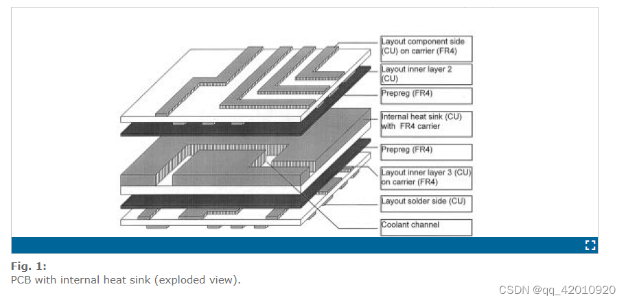
Fig. 1 represents the basic structure of a five-layer PCB which is an example of a liquid-cooled PCB. Technological processes are left out. When starting with the above-mentioned concept of channel formation, it has been found that the copper foil in use was too weak to maintain well-defined channel cross sections. Therefore, we manufacture a suitable internal layer. This one is formed through multilayer bonding of a specific metal-core prepreg acting as an FR4 substrate with a 400-μm copper foil (Fig. 1). Please note that the term “metal-core prepreg”-although technically commonly used-is misleading. In spite of its name, a metal-core prepreg does not contain any metal but is used to be laminated or to be bonded to relatively thick metal layers. After multilayer bonding, this copper foil is etched so that microchannels of a cross section of 400 μm by 1000 μm are formed. Etching the channel occurs analog to the usual internal layer structuring. Several etching processes must be run to achieve the depth of 400 μm. A typical cross section of such a channel is seen in Fig. 2. The edge of the micro channel is one of the most crucial points of the cooling system within the PCB. An advantage of material system copper-FR4 favors this work: the linear coefficient of expansion of both materials is approximately identical. Nevertheless, a careful compliance with the optimum bonding parameters (pressure, time, temperature profile) is mandatory. Due to underetching, a copper-to-channel boundary is formed with an area larger than in the case of anisotropic etching. Therefore, a more favorable heat transfer is obtained. In contrast to the original concept, the fabrication of these channels is reliable and reproducible. Both sides of this internal heat sink are covered with prepregs. The no-flow prepreg toward the component side acts as stabilization and insulation for the inner layout layers to the copper.
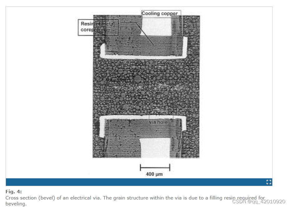
While bonding prepregs, one requires high temperatures and pressures. The flow of the resin part is the essential task of the prepregs during this process. During the complete polymerization of the resin, it combines itself with the neighboring copper layer. In the case of carefully kept process parameters, the firmness and the tightness is sufficient. The planarity of the individual layers is very important for the bonding process of a multilayer process. However, the commercially available base materials essentially comply with these demands today. A simplified layer sequence is reproduced in Fig. 3. It shows a technological application of the underlying principle, namely, a three-layer-structure as an example of the simplest design variant. In the next step, vias have to be created to form electrical connections between the solder and component sides or to inner layers. One has to distinguish between electrical vias and so-called thermal vias. Electrical vias passing the new heat sink must be safely insulated. In the following, we describe the production, in particular, of these vias in more detail (Fig. 4).
电路板和通道的制造 图 1 表示五层 PCB 的基本结构,它是液冷 PCB 的一个示例。技术过程被忽略了。当从上述通道形成的概念开始时,发现使用的铜箔太弱而无法保持明确的通道横截面。因此,我们制造了合适的内层。这是通过多层粘合形成的特定金属芯预浸料作为 FR4 基板与 400-μm 铜箔(图 1)。请注意,术语“金属芯预浸料”——尽管在技术上常用——具有误导性。尽管它的名字,金属芯预浸料不含任何金属,但用于层压或粘合到相对较厚的金属层。在多层接合之后,对该铜箔进行蚀刻,从而形成横截面为400μm×1000μm的微通道。蚀刻通道类似于通常的内层结构。必须运行几个蚀刻工艺才能达到 400 μm 的深度。这种通道的典型横截面如图 2 所示。微通道的边缘是 PCB 内冷却系统的最关键点之一。材料系统铜-FR4 的一个优势有利于这项工作:两种材料的线性膨胀系数大致相同。然而,必须仔细遵守最佳粘合参数(压力、时间、温度曲线)。由于蚀刻不足,形成面积大于各向异性蚀刻情况下的铜-沟道边界。因此,获得了更有利的热传递。与原始概念相比,这些通道的制造是可靠且可重复的。该内部散热器的两侧都覆盖有预浸料。朝向组件侧的无流动预浸料充当内部布局层与铜的稳定和绝缘。在粘合预浸料时,需要高温和高压。树脂部分的流动是此过程中预浸料的基本任务。在树脂完全聚合期间,它与相邻的铜层结合。在精心保存工艺参数的情况下,牢固度和密封性就足够了。各个层的平面度对于多层工艺的键合工艺非常重要。然而,目前市售的基材基本上符合这些要求。图 3 再现了简化的层序列。它显示了基本原理的技术应用,即三层结构作为最简单设计变体的示例。在下一步中,必须创建通孔以在焊料和组件侧面或内层之间形成电连接。必须区分电通孔和所谓的热通孔。通过新散热器的电气通孔必须安全绝缘。在下文中,我们将更详细地描述这些通孔的生产,特别是(图 4)。
One starts by drilling an oversized hole into the FR4 cooling copper structure. The size of the hole is identical to the distance between the two white areas in Fig. 4 labeled “cooling copper.” For electrical insulation, this hole is filled with metal-core-prepreg resin. Then, the other layers are assembled. For the sake of simplicity, just one prepreg layer-on top of the copper-has been used in Fig. 4. Now, a concentric second hole of smaller diameter is drilled and plated. Prior to the drilling process, a special X-ray-controlled drilling machine localizes the inserted targets in the internal layer and drills two registration holes. These are used for the precise positioning of the multilayer on the drilling machine. The subsequent metallization of the vias does not occur selectively, but over the entire surface of the PCB. That means that the copper layer is simultaneously galvanically reinforced on the external layers. Since small tolerances can be kept, high insulation resistances between via and cooling copper can be maintained.
We still have to a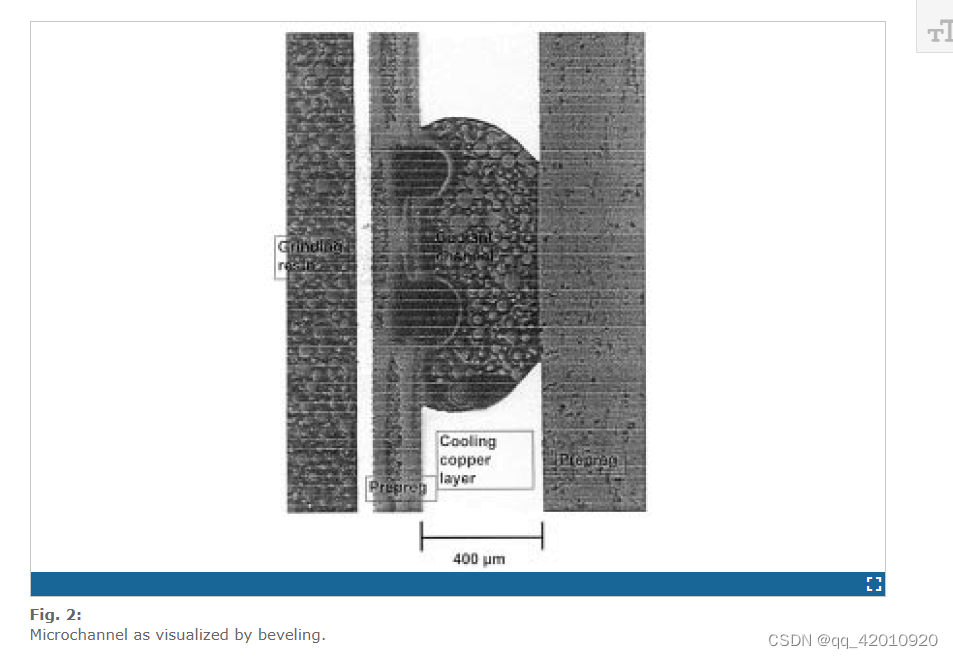 dd the function of the thermal vias. These are metal plated through holes or blind holes which connect the external copper foil with the internal cooling copper layer. These holes are simultaneously inserted with others through holes after bonding the multilayer structure. As the name suggests, their purpose is to improve the heat transfer from the heat source to the cooling channel. This transfer can occur along three paths: 1) in the vertical direction from the device to a channel placed underneath; 2) in the vertical direction from the device to the inner cooling copper, then in the horizontal direction toward the microchannel; and 3) in the horizontal direction from the device through the outer copper, then in the vertical direction along the via copper, and again in the horizontal direction through the inner copper to the microchannel.
The computer simulation of the heat dissipation yielded the following: every path of the conduction of the component to the channel which is disturbed by FR4 material has an extremely high temperature gradient. For optimum dissipation of heat, a continuous connection must consist of copper. Although this path is longer, nevertheless, this construction offers better heat dissipation. The demand of minimum thermal resistance implies a maximum inner copper wall height. A value of 400 μm is a good tradeoff between low thermal resistance and handling requirements.
首先是在 FR4 冷却铜结构中钻一个超大的孔。孔的大小与图 4 中标记为“冷却铜”的两个白色区域之间的距离相同。对于电绝缘,该孔填充有金属芯预浸树脂。然后,组装其他层。为简单起见,在图 4 中只使用了铜顶部的一个预浸料层。现在,钻了一个较小直径的同心第二个孔并进行电镀。在钻孔过程之前,一台特殊的 X 射线控制钻孔机将插入的目标定位于内层并钻出两个配准孔。这些用于在钻孔机上精确定位多层。通孔的后续金属化不是选择性地发生,而是在 PCB 的整个表面上发生。这意味着铜层同时在外层上进行了电镀加固。由于可以保持小公差,因此可以保持通孔和冷却铜之间的高绝缘电阻。我们仍然需要添加散热孔的功能。这些是连接外部铜箔和内部冷却铜层的镀金属通孔或盲孔。在粘合多层结构之后,这些孔与其他通孔同时插入。顾名思义,它们的目的是改善从热源到冷却通道的热传递。这种传输可以沿着三个路径发生: 1) 从设备到位于下方的通道的垂直方向; 2)从设备垂直方向到内部冷却铜,然后在水平方向朝向微通道; 3)从器件水平方向通过外层铜,然后在垂直方向上沿着通孔铜,再在水平方向上通过内层铜到达微通道。散热的计算机模拟得出以下结论:组件传导到通道的每条路径都受到 FR4 材料的干扰,具有极高的温度梯度。为了最佳散热,连续连接必须由铜组成。尽管这条路径更长,但是,这种结构提供了更好的散热。最小热阻的要求意味着最大的内铜壁高度。 400 μm 的值是低热阻和处理要求之间的良好折衷。
Results
A test board based on the above manufacturing process is seen in Fig. 5. The large white area represents the cooling section which is entirely separated from the circuit section. It should be pointed out that any type of devices can be placed on the cooling area. For example, for a square surface-mounted device (SMD), the outer copper area has just to be reduced to the inner area size of the device.
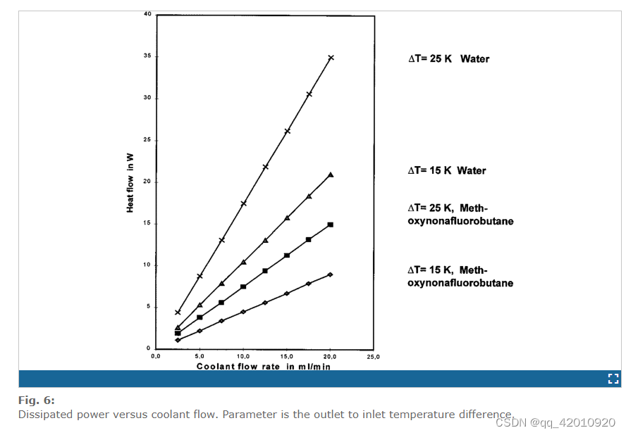
In a first test, the required coolant flow rate versus generated heat power for a constant temperature difference between outlet and inlet has been determined (Fig. 6). From these results, it is concluded that a safe operation up to a power of 20 W per channel and heat source is guaranteed. It is also seen that, in spite of the disadvantages, water is preferred to methoxynon-afluorobutane, as discussed below.
Fig. 7 gives some additional information on the pressure loss developed by a given flow rate. Of course, this graph is valid for the chosen geometry only; however, the data give a general feeling for the choice of the required pump capacity.
基于上述制造工艺的测试板如图5所示。大的白色区域代表冷却部分,它与电路部分完全分开。需要指出的是,任何类型的设备都可以放置在冷却区域上。例如,对于方形表面贴装器件 (SMD),外部铜面积只需减小到器件的内部面积大小。在第一个测试中,已经确定了出口和入口之间恒定温差下所需的冷却剂流量与产生的热功率的关系(图 6)。从这些结果可以得出结论,可以保证在每个通道和热源的功率高达 20 W 的情况下安全运行。还可以看出,尽管有缺点,但水比甲氧基非-氟代丁烷更优选,如下所述。
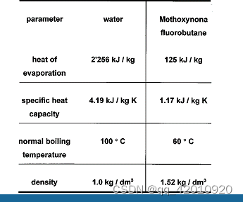
As partially anticipated, the choice of the coolant is another point of consideration. We have concentrated on two liquids, namely, water and methoxynonafluorobutane. We briefly list the advantages of either material: water offers higher evaporative heat power, higher specific heat capacity, and lower pressure loss. On the other side, the advantages of methoxynonafluorobutane are lower electrical conductivity, neutral to ozone, lower boiling point, and applicability of evaporative cooling. Table I is a brief compilation of the data essential for the cooling performance of the two liquids. It must be noted, however, that the advantages of methoxynonafluorobutane are overridden by far by those of water.
It is obvious that a large quantity of heat flow paths exists. As a result, an optimization of the number and placement of the thermovias is mandatory. Fig. 8 exhibits four configurations, with one and two cooling channels, with different via densities and local patterns. The optimum cooling capability is obtained-as expected-for the highest via density, best matching to the device shape, and highest channel number [Fig. 8(a)]. The data of Figs. 6 and 7 were obtained for this via and channel configuration.
With the presented solution, we are able to eliminate thermal powers in components of the same amount as with cooling elements (approximately 20–30 W per component). However, this heat dissipation can be readjusted very quickly, unlike in the case of cooling elements. While cooling, the close vicinity of the component is not heated up. The enormous space required for an otherwise necessary cooling element and a fan (approximately 800 em3) immediately placed on the component is no longer required. The same advantage holds for the mass problem which normally occurs in oscillating devices.
The mentioned advantages of the micro cooling system must be paid with a minimum periphery. This consists of an external liquid cooling device, a diaphragm pump, a tube and connector system, and the temperature controlling. In the case of a compressed construction, the cooling system requires a volume of not more than 1 dm3 per 30 W.
Conclusion
We have developed a new cooling concept based on an FR4-compatible process. The typical heat power dissipation is 20 W per cooling channel and device. The system is suited for industrial use and already employed in various applications.
The problems for further investigations are the optimization of the internal channel cross sections, the optimization of the via placement, and the development of a modular general-purpose cooling layout.
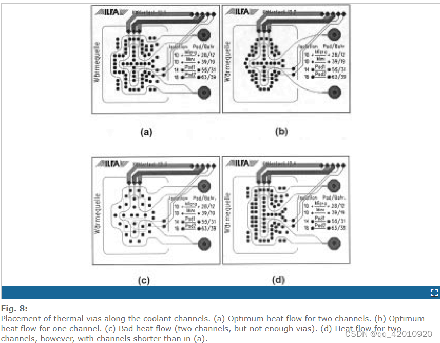
很明显,存在大量的热流路径。因此,必须优化热通孔的数量和位置。图 8 展示了四种配置,具有一个和两个冷却通道,具有不同的通孔密度和局部图案。正如预期的那样,获得了最佳冷却能力,以获得最高的通孔密度、与器件形状的最佳匹配以及最高的通道数 [图。 8(a)]。图的数据。对于这种通孔和通道配置,获得了图 6 和图 7。
使用所提出的解决方案,我们能够消除与冷却元件相同数量的组件中的热功率(每个组件大约 20-30 W)。但是,与冷却元件不同,这种散热可以非常快速地重新调整。在冷却时,组件的附近不会被加热。不再需要立即放置在组件上的原本必需的冷却元件和风扇(约 800 em3)所需的巨大空间。同样的优点也适用于通常发生在振荡装置中的质量问题。
微冷却系统的上述优点必须以最小的外围来支付。这包括一个外部液体冷却装置、一个隔膜泵、一个管子和连接器系统以及温度控制。在压缩结构的情况下,冷却系统需要的体积不超过每 30 W 1 dm3。
我们开发了基于 FR4 兼容工艺的新冷却概念。每个冷却通道和设备的典型热功率耗散为 20 W。该系统适用于工业用途,并已用于各种应用。
进一步研究的问题是内部通道横截面的优化、通孔布局的优化以及模块化通用冷却布局的开发。


 被折叠的 条评论
为什么被折叠?
被折叠的 条评论
为什么被折叠?
 到【灌水乐园】发言


