


Abstract:
The electronic industry has a growing need for efficient heat dissipation mechanisms such as micro heat exchanger systems. This active cooling approach requires the integration of microfluidic components near the main heat sources of the electronic devices. Despite the investigation of several micro-cooling configurations, their commercial utilization by the electronic industry is rather limited due to complex fabrication and integration methods. Here, we present the integration of cylindrical microchannels fabricated by direct-write assembly in printed circuit board layouts for a micro heat exchanger application. The thermal performance of the manufactured prototype was characterized with respect to the fluid flow rate. The original fabrication and integration approaches presented here show high potential for efficient, compact, and low-cost micro heat exchangers for the electronic industry.
电子行业对高效散热机制(例如微型热交换器系统)的需求不断增长。这种主动冷却方法需要在电子设备的主要热源附近集成微流体组件。尽管研究了几种微冷却配置,但由于复杂的制造和集成方法,它们在电子行业的商业应用相当有限。在这里,我们展示了通过直接写入组装制造的圆柱形微通道在用于微型热交换器应用的印刷电路板布局中的集成。所制造原型的热性能以流体流速为特征。这里介绍的原始制造和集成方法显示出用于电子行业的高效、紧凑和低成本微型热交换器的巨大潜力。
THERMAL management has become a major limitation for the electronic industry. The utilization of extremely small transistors at high operating frequencies (∼GHz) generate a significant amount of heat which is exceeding the capacity of conventional heat removal techniques. The lack of heat dissipation yields higher operating temperatures that increase the risk of electrical failures in the device. This concern is not only problematic for the electronic industry [1] but also for the development of miniaturized robots [2] and the design of aerospace structures [3]. For many applications, air cooling mechanisms are not sufficient or simply impossible and other cooling technologies have to be used. Fluid cooling (e.g., water) offers a thermal conductivity and a specific heat capacity 25 and 4 times superior than air, respectively. The passive or active circulation of liquid could be used to transfer the heat from a specific location to another location where heat dissipation becomes more effective. For example, the heat generated by all the main electronic components of a computer could be transferred to a fluid and then transported to a single heat dissipation system, reducing the number of fans while lowering the noise level. Thus, electronic manufacturers have an increasing interest in passive micro heat pipe [4], [5] and active micro heat exchanger technologies since they enable the creation of compact and efficient heat removal systems located close to the heat source.
The cooling of electronic components using micro heat exchangers is a promising approach [6]–[7][8][9]. A micro heat exchanger is an active system where the heat is transferred to a fluid circulating inside a microchannel (i.e., channel with a hydraulic diameter smaller than 1 mm). The system is usually composed of a pump for fluid circulation, a heat source, a heat sink and a network of microchannels. Previous work demonstrated an efficient micro heat exchanger cooling system with a low thermal resistance and a high heat dissipation capacity reaching 750 W/cm2 [10]. The cooling efficiency of the micro heat exchanger strongly depends on the fluid flow rate, the thermal properties of the cooling fluid, the hydraulic diameter of the microchannel and the surface and the distance of the microchannel network to the heat sources. In addition, the utilization of integrated microchannels inside a printed circuit board (PCB) will enable a tight coupling with the heat source while minimizing the thermal resistance. Exposed paddle packages (i.e., packaging technique where metallic die paddles are exposed on the die) exhibit better thermal characteristics compared to other packaging techniques but the heat flux absorbed by the ground planes is not removed. This heat flux in the board may lead to an increase of temperature over time leading to malfunctions or failures of the device. Thus, the heat removal of conventional PCB such as copper/FR4 requires enhancement in order to facilitate the fabrication of high power electronic devices.
The main manufacturing processes used to build microchannels for micro heat exchanger are LIGA (i.e., German acronym for RontgenLIthographie Galvanik Abformung meaning X-ray lithography electrodeposition and molding), chemical etching, stereolithography, and micromachining [11]. Silicon etching is the most reported technique for the fabrication of microchannels with rectangular, trapezoidal, or triangular cross section. However, the integration of microfluidic components fabricated by chemical etching, LIGA, and stereolithography is not compatible with FR4 PCB manufacturing. The main challenges are the materials and chemical used and the required process for bonding between the micro heat exchanger and the electronic device. Micromachining of copper was successfully used [12] for the fabrication of microchannel on copper/FR4 boards and is occasionally used by the electronic industry. Though, the micromachining process is limited regarding the possible microchannel cross-sectional geometry.
This paper presents the fabrication of circular cross-section microchannels (∼200 and 500 μm in diameter) and their integration inside the layers of a PCB for micro heat exchanger applications. The fabrication of the microchannels by direct-write assembly inside PCBs enables a tight thermal coupling to the heat sources. This customizable approach can use the Gerber files to define the microchannel path and avoid the vias. The thermal efficiency of a prototype with a 500-μm-diameter microchannel was experimentally characterized and showed promising performance at high flow rates.
热管理已成为电子行业的主要限制。在高工作频率(~GHz)下使用极小的晶体管会产生大量热量,这超出了传统散热技术的能力。缺乏散热会产生更高的工作温度,从而增加设备发生电气故障的风险。这种担忧不仅对电子行业 [1] 存在问题,而且对微型机器人 [2] 的开发和航空航天结构的设计 [3] 也存在问题。对于许多应用,空气冷却机制是不够的或根本不可能,必须使用其他冷却技术。流体冷却(例如水)提供的热导率和比热容分别是空气的 25 倍和 4 倍。液体的被动或主动循环可用于将热量从特定位置传递到另一个散热变得更有效的位置。例如,计算机所有主要电子元件产生的热量都可以转移到流体中,然后输送到单个散热系统,从而减少风扇数量,同时降低噪音水平。因此,电子制造商对无源微型热管 [4]、[5] 和有源微型换热器技术越来越感兴趣,因为它们能够在靠近热源的位置创建紧凑且高效的散热系统。
使用微型热交换器冷却电子元件是一种很有前途的方法 [6]-[7][8][9]。微型热交换器是一种主动系统,其中热量被传递到在微通道(即水力直径小于 1 毫米的通道)内循环的流体。该系统通常由用于流体循环的泵、热源、散热器和微通道网络组成。以前的工作展示了一种高效的微型换热器冷却系统,该系统具有低热阻和高散热能力,达到 750 W/cm2 [10]。微换热器的冷却效率很大程度上取决于流体流速、冷却流体的热特性、微通道和表面的水力直径以及微通道网络到热源的距离。此外,利用印刷电路板 (PCB) 内部的集成微通道将实现与热源的紧密耦合,同时将热阻降至最低。与其他封装技术相比,裸露焊盘封装(即金属管芯焊盘暴露在管芯上的封装技术)表现出更好的热特性,但接地层吸收的热通量并未消除。电路板中的这种热通量可能会导致温度随时间升高,从而导致设备出现故障或故障。因此,传统PCB(如铜/FR4)的散热需要增强,以促进大功率电子设备的制造。
用于构建微换热器微通道的主要制造工艺是 LIGA(即,德语首字母缩写为 RontgenLIthographie Galvanik Abformung,意思是 X 射线光刻电沉积和成型)、化学蚀刻、立体光刻和微加工 [11]。硅蚀刻是用于制造具有矩形、梯形或三角形横截面的微通道的最报道的技术。然而,通过化学蚀刻、LIGA 和立体光刻技术制造的微流体组件的集成与 FR4 PCB 制造不兼容。主要挑战是所使用的材料和化学品以及微型热交换器和电子设备之间粘合所需的工艺。铜的微加工已成功用于 [12] 在铜/FR4 板上制造微通道,并且偶尔被电子工业使用。但是,微加工过程在可能的微通道横截面几何形状方面受到限制。
本文介绍了圆形横截面微通道(直径约 200 和 500 μm)的制造及其在 PCB 层内的集成,用于微热交换器应用。通过 PCB 内的直接写入组件制造微通道可以实现与热源的紧密热耦合。这种可定制的方法可以使用 Gerber 文件来定义微通道路径并避免过孔。具有 500 μm 直径微通道的原型的热效率经过实验表征,并在高流速下显示出良好的性能。
Experimental Procedure and Materials
A. Substrate Preparation
A double-layered Cu/FR4 sheet of 350 μm of thickness (Cu=75 μm, FR4=200 μm) was used for the prototype fabrication. Copper was etched from the substrate on one side of the sheets using a PCB milling (Protomat S95, LPKF) to form heating circuits. Two prototypes were made with lines width of 200 μm and 500 μm, respectively. A thin resin film (∼40-200 μm) was then deposited and polished on the circuit for electrical isolation. Note that this insulation layer is not necessary if the microchannels are directly built over the ground plane and are not crossing electrical lines, and the cooling fluid used is a dielectric.
B. Microchannel Fabrication
Microchannels were directly built over the traces of copper by direct-write assembly. This approach consists of the robotic deposition of an ink for the free-form fabrication of various structures such as periodic ceramic structures [13] or fluidic 3-D micromixers [14]. The direct-write procedure for the creation of microchannels is based on the robotic deposition of a fugitive organic ink [15] on a substrate as illustrated in Fig. 1.
实验程序和材料
A. 基板准备
350 μm 厚度的双层 Cu/FR4 片材(Cu=75 μm,FR4=200 μm)用于原型制造。使用 PCB 铣削 (Protomat S95, LPKF) 从基板一侧蚀刻铜以形成加热电路。制作了两个原型,线宽分别为 200 μm 和 500 μm。然后在电路上沉积并抛光薄树脂膜(~40-200μm)以进行电隔离。请注意,如果微通道直接构建在接地平面上并且不与电线交叉,并且使用的冷却液是电介质,则不需要此绝缘层。
B. 微通道制造
微通道通过直接写入组装直接构建在铜迹线上。这种方法包括机器人沉积墨水,以自由形式制造各种结构,例如周期性陶瓷结构 [13] 或流体 3-D 微混合器 [14]。用于创建微通道的直接写入程序基于在基板上自动沉积逃逸有机墨水 [15],如图 1 所示。
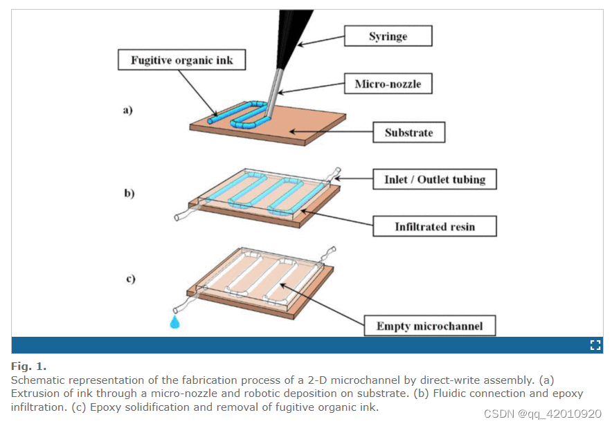
The ink is contained in a syringe barrel and consists of a mixture of 40% by weight of microcrystalline wax and 60% by weight of petroleum jelly. The paste-like material was extruded through a cylindrical micronozzle (200 or 500 μm in diameter, Stainless-steel precision tips, EFD) under constant pressure. The ink deposition pattern was performed at constant velocity according to the circuit drawings Alignment marks were etched on the copper in order to position the tip of the nozzle relative to the circuit prior to the ink deposition. The deposited ink pattern was then infiltrated [Fig. 1(b)] with a low-viscosity resin (ratio 2.5:1, Epon-828 and Epi-cure 3274, Shell Chemicals) at ambient conditions.
C. Micro Heat Exchanger Assembly
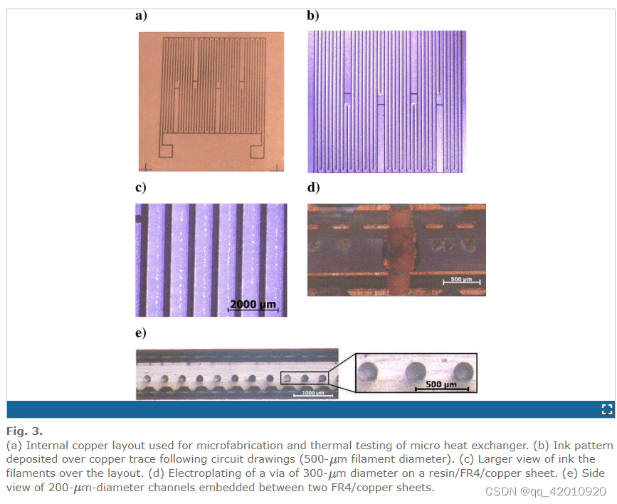
Upon curing, a second laminated sheet of Cu/FR4 was glued to the circuit using the same epoxy resin for the assembly of the multilayer PCB (Fig. 2). Holes of 300 μm and 2 mm in diameter were drilled on the board for the creation of thermal and electrical vias. The fully assembled micro heat exchangers (microchannel diameter of 200 or 500 μm) are depicted in Fig. 3. Fig. 3(a) presents the outlines etched on the internal layout of the PCBs. The channel used was 1.45 m long and covered a planar area of 7.25 cm2. A chemical electroplating (Contact II, LPKF) was performed for a successful coating of copper over the resin/FR4 layers as shown in Fig. 3(d). Fig. 3(e) is a side view of the middle of the PCB showing that the circularity of the microchannel cross section was maintained during the fabrication and integration processes. The inner wall surface of the microchannel had a root-mean-square roughness of 13.3 ± 6.5 nm [14].
墨水装在注射器筒中,由 40%(重量)微晶蜡和 60%(重量)凡士林的混合物组成。在恒定压力下将糊状材料通过圆柱形微喷嘴(直径 200 或 500 μm,不锈钢精密尖端,EFD)挤出。根据电路图以恒定速度进行油墨沉积图案在铜上蚀刻对准标记,以便在油墨沉积之前将喷嘴的尖端相对于电路定位。然后渗透沉积的墨水图案[图。 1(b)]在环境条件下与低粘度树脂(比率2.5:1,Epon-828和Epi-cure 3274,Shell Chemicals)。
C. 微型换热器组件
固化后,使用相同的环氧树脂将第二块 Cu/FR4 层压板粘合到电路上,用于组装多层 PCB(图 2)。在板上钻出 300 μm 和 2 mm 直径的孔,用于创建热和电通孔。完全组装的微型热交换器(微通道直径为 200 或 500 μm)如图 3 所示。图 3(a) 显示了蚀刻在 PCB 内部布局上的轮廓。使用的通道长 1.45 m,覆盖面积为 7.25 cm2。进行化学电镀(Contact II,LPKF)以在树脂/FR4 层上成功涂覆铜,如图 3(d)所示。图 3(e) 是 PCB 中间的侧视图,显示了在制造和集成过程中微通道横截面的圆形度得以保持。微通道内壁表面的均方根粗糙度为 13.3 ± 6.5 nm [14]。
D. Fluidic Connections
After the board assembly, the two extremities of the encapsulated ink pattern were glued to micro-tubes (S-54-HL, Tygon) with either an inner diameter of 200 μm or 500 μm. Then, the board was heated at moderate temperature (∼348 K) and the melted ink was removed under a vacuum at one end of the micro-tubing. Finally, hot water was injected for a few seconds in the microchannel in order to completely remove the ink [Fig. 1(c)].
E. Thermal Setup
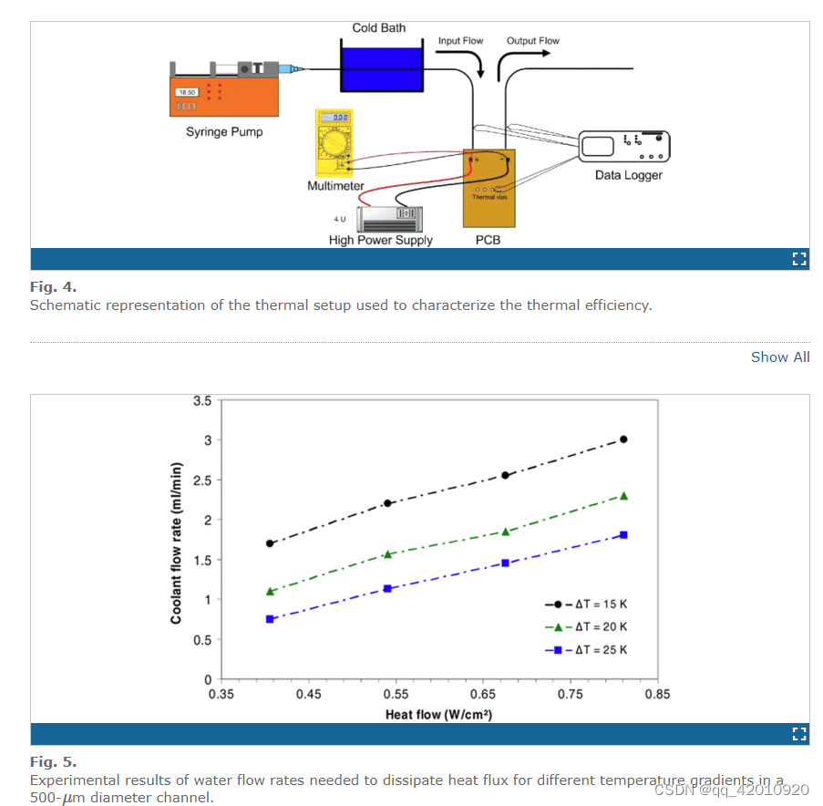
Thermal experiments were performed on a four layer PCB containing a 500-μm-diameter microchannel in order to demonstrate the novel fabrication and integration processes and characterize the thermal efficiency of our micro heat exchanger.
The thermal testing setup is shown in Fig. 4. The inside etched copper layer is electrically connected through vias and is used to generate the heat flux. In the present case, distilled water was used as the cooling fluid. The circuit has been embedded in a polymer matrix to minimize the heat dissipated by convection during the experiment. The temperature reading was done with type-T thermocouples connected to the inlet/outlet of the channel and to a via located at the center of the circuit to measure its average temperature. The water was injected at a temperature of 284 ±1 K in order to reach the desired temperature gradients between the circuit and the input fluid temperature.
The following procedure was used during the thermal experiments. First, a high current (DCS12-250E, Sorensen) was applied while the voltage was monitored at the terminals of the circuit. A syringe pump (NE-1000, Pump Systems, Inc.) was used to flow the cooling water at a desired flow rate. The temperatures were monitored and recorded using thermocouples linked to a data acquisition system (HH506R, Omega). The thermocouples measured the fluid temperature at the entrance and exit of the embedded microchannel, and the temperature of the circuit located in the center of the board. Finally, the flow rate imposed by the syringe pump was manually adjusted and maintained constant in order to achieve the specific temperature gradients (i.e., 15 K, 20 K, and 25 K) between the input fluid temperature and the circuit (ΔT). The adjusted flow rates were recorded after a few minutes when the steady state condition was reached.
SECTION III.
Results and Discussion
A. Thermal Results
The current of the power supply was set to generate a power of 3 W, 4 W, 5 W, and 6 W in the internal circuit having an area of 7.25 cm2. Fig. 5 presents the adjusted fluid flow rates required to keep a temperature gradient between the circuit and the input fluid at 15 K, 20 K, and 25 K. Fluid flow rates ranging from 0.75 to 3 ml/min were necessary to reach the desired temperature gradients with a linear dependence. Assuming that this linear regime is maintained at higher flow rates, the thermal performance of the prototype could be extrapolated before turbulent flow occurs (i.e., when the linear regime was lost).
D. 流体连接
在电路板组装之后,将封装的墨水图案的两个末端粘合到内径为 200 μm 或 500 μm 的微管(S-54-HL,Tygon)上。然后,将板在中等温度(~348 K)下加热,并在真空下在微管的一端去除熔化的墨水。最后,在微通道中注入热水几秒钟以完全去除墨水[图。 1(c)]。
E. 热设置
在包含 500 μm 直径微通道的四层 PCB 上进行热实验,以展示新颖的制造和集成工艺并表征我们的微型热交换器的热效率。
热测试装置如图 4 所示。内部蚀刻铜层通过通孔进行电连接,用于产生热通量。在本例中,蒸馏水用作冷却液。该电路已嵌入聚合物基质中,以最大限度地减少实验过程中对流散发的热量。温度读数是通过连接到通道入口/出口的 T 型热电偶和位于电路中心的通孔来测量其平均温度来完成的。以 284 ±1 K 的温度注入水,以达到回路和输入流体温度之间的所需温度梯度。
在热实验期间使用以下程序。首先,施加大电流(DCS12-250E,Sorensen),同时监测电路端子处的电压。使用注射泵(NE-1000,Pump Systems,Inc.)使冷却水以所需的流速流动。使用连接到数据采集系统(HH506R,Omega)的热电偶监测和记录温度。热电偶测量嵌入式微通道入口和出口处的流体温度,以及位于电路板中心的电路温度。最后,手动调节注射泵施加的流速并保持恒定,以实现输入流体温度和回路 (ΔT) 之间的特定温度梯度(即 15 K、20 K 和 25 K)。在达到稳态条件的几分钟后记录调整后的流速。
第三节结果与讨论
A. 热结果
电源电流设定为在面积为7.25cm2的内部电路中产生3W、4W、5W和6W的功率。图 5 显示了将回路和输入流体之间的温度梯度保持在 15 K、20 K 和 25 K 所需的调整后流体流速。流体流速范围为 0.75 到 3 ml/min 是达到所需的必要条件温度梯度与线性相关。假设这种线性状态保持在较高的流速下,原型的热性能可以在湍流发生之前外推(即,当线性状态消失时)。
The Reynolds number is the dimensionless ratio of inertial to viscous forces and is calculated using
Re=ρDhuη=Dhuυ(1)
where Dh is the hydraulic diameter, u is the average velocity of the fluid inside the channel, ρ is the density of the fluid, η is the dynamic viscosity, and υ is the kinematic viscosity of the fluid which is temperature dependent.
At the highest flow rate used during the experiments (i.e., 3 ml/min), the Reynolds number reached a value of only 178 and laminar flow was maintained. Fig. 6 shows the Reynold numbers with respect to the average fluid temperature for two different flow rates (i.e., 1.8 and 3 ml/min). The thermal performance can then be extrapolated for a flow rate of 17 and 20 ml/min, where turbulent flow is expected to occur (i.e., Re ∼1000 for most situations [16]). With a flow rate of 17 ml/min and a temperature gradient of 25 K, an heat flow dissipation of 6.73 W/cm2 using the linear relation measured from the thermal experiments (Fig. 5) is predicted. At a flow rate of 20 ml/min and a temperature gradient of 15 K, the predicted heat dissipation is 6.23 W/cm2. As expected, the higher temperature gradient will dissipate more heat at a lower coolant flow rate. However, higher operating temperatures will also increase the Reynolds number and the risk of turbulent flows.
其中 Dh 是水力直径,u 是通道内流体的平均速度,ρ 是流体的密度,η 是动态粘度,υ 是流体的运动粘度,它与温度有关。
在实验期间使用的最高流速(即 3 ml/min)下,雷诺数仅达到 178 并保持层流。图 6 显示了两种不同流速(即 1.8 和 3 ml/min)下相对于平均流体温度的雷诺数。然后可以将热性能外推为 17 和 20 ml/min 的流速,其中预计会发生湍流(即,对于大多数情况 [16],Re 约为 1000)。在 17 ml/min 的流速和 25 K 的温度梯度下,使用热实验测量的线性关系(图 5)预测的热流耗散为 6.73 W/cm2。在 20 ml/min 的流速和 15 K 的温度梯度下,预计散热量为 6.23 W/cm2。正如预期的那样,较高的温度梯度将以较低的冷却剂流速消散更多的热量。然而,更高的工作温度也会增加雷诺数和湍流的风险。
B. Pressure Drop
The pressure drop along a channel needs to be within the capacity the micro-pump used with the micro heat exchanger system. During our thermal experiments, leakage was observed at flow rates >6 ml/min due to fluidic connection problems and high pressure at the fluid inlet. Considering the operating temperature range and the desired flow rate for a given heat dissipation, the pressure drop can be estimated. For circular microchannels, the pressure drop is given by
ΔP=RefηL2D2hu(2)
where L is the length of the channel and f is the Darcy friction factor. This factor for laminar flows is defined by
f=64/Re.(3)
Substituting (3) into (2) gives
ΔP=32ηLD2hu.(4)
沿通道的压降需要在与微型热交换器系统一起使用的微型泵的容量范围内。在我们的热实验中,由于流体连接问题和流体入口处的高压,在 >6 ml/min 的流速下观察到泄漏。考虑到给定散热的工作温度范围和所需的流量,可以估计压降。对于圆形微通道,压降由下式给出
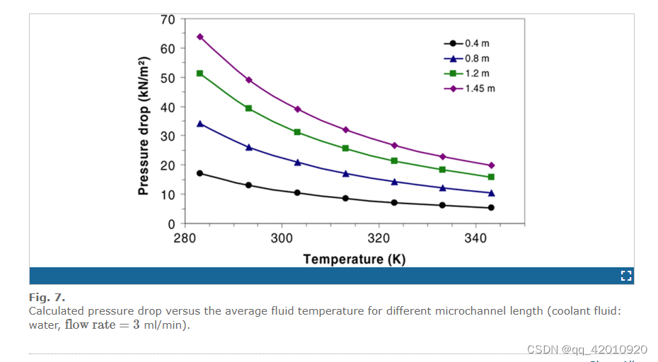
As described by (4), this estimation of the pressure drop is a function of the length of the channel, its hydraulic diameter, the dynamic viscosity, and the velocity of the fluid. At constant temperature, the pressure drop increases linearly along a channel and the slope depends on the fluid flow rate. For a flow rate of 3 ml/min and an average fluid temperature of 298 K, the pressure drop reaches a value as high as ∼42 kN/m2 at the end of the channel (diameter=500 μm). The dynamic viscosity of water is temperature dependent [17] and this variation affects the pressure drop along a channel as shown in Fig. 7. For a temperature gradient of 15 K, the pressure drop at the end of the microchannel during our experiments is estimated at ∼41 kN/m2 as opposed to ∼33 kN/m2 for a gradient of 25 K. Fig. 7 also shows that the length of the channel has less effect on the pressure drop as the temperature increases. This diminution of the pressure drop promotes the operation of the cooling system at the highest possible temperature while staying below the junction temperature and turbulent flow transition.
如 (4) 所述,该压降估计是通道长度、其水力直径、动态粘度和流体速度的函数。在恒定温度下,压降沿通道线性增加,斜率取决于流体流速。对于 3 ml/min 的流速和 298 K 的平均流体温度,压降在通道末端(直径 = 500 μm)达到高达 ∼42 kN/m2 的值。水的动态粘度取决于温度 [17],这种变化会影响沿通道的压降,如图 7 所示。对于 15 K 的温度梯度,我们的实验期间微通道末端的压降是估计的41 kN/m2,而 25 K 的梯度为 33 kN/m2。图 7 还表明,随着温度的升高,通道的长度对压降的影响较小。这种压降的减小促进了冷却系统在可能的最高温度下运行,同时保持低于结温和湍流过渡。
Conclusion
We have successfully used a new microfabrication technique based on direct assembly of a fugitive organic ink to build circular microchannels inside PCBs. The fabrication process is compatible with PCBs manufacturing process or requires minor modifications. This process could be combined to exposed paddles packages, for instance, for higher heat dissipation with low thermal resistance. The routing of the channels is customizable and can be adjusted to the specifications of a circuit design to achieve the best thermal coupling with high power components. Direct writing is a relatively low cost production technique and recent work [19] has already enhanced the manufacturing capability of the direct write process with a writing speed of up to 100 mm/s for two dimensional microchannels. Experiments have been conducted with one channel with a diameter of 500 μm using low flow rates. The results show promises for this technique with a heat dissipation of 0.81 W/cm2 at only 3 ml/min. Under laminar flow, the extrapolated heat dissipation is estimated at 6.7 W/cm2 for a flow rate of 17 ml/min and a temperature gradient of 25 K. The diameter, length, and number of channel deployed need to be adjusted according to the heat sink and the micropump used and the desired operating temperature for an efficient cooling.
结论
我们已经成功地使用了一种基于直接组装逃逸有机墨水的新型微细加工技术,在 PCB 内部构建了圆形微通道。制造过程与 PCB 制造过程兼容或需要进行少量修改。例如,该工艺可以与裸露焊盘封装相结合,以实现更高的散热和低热阻。通道的布线是可定制的,并且可以根据电路设计的规格进行调整,以实现与高功率组件的最佳热耦合。直写是一种成本相对较低的生产技术,最近的工作 [19] 已经提高了直写工艺的制造能力,二维微通道的写入速度高达 100 mm/s。已经使用低流速对一个直径为 500 μm 的通道进行了实验。结果表明,这种技术有望在仅 3 ml/min 的情况下散热 0.81 W/cm2。在层流下,对于 17 ml/min 的流速和 25 K 的温度梯度,外推散热估计为 6.7 W/cm2。部署的通道的直径、长度和数量需要根据热量进行调整水槽和使用的微型泵以及有效冷却所需的工作温度。


 被折叠的 条评论
为什么被折叠?
被折叠的 条评论
为什么被折叠?
 到【灌水乐园】发言


