


abstract
The 3D-packaging technology makes it possible to stack the PCBs on top ofeach other and thus makefull use ofthe third dimension. A unique space between the stacked PCB layers enables a reproducible technology without shortcuts or unconnected bumps. New applications in 3D-PDB-packages, called PCBMEMS can be realized with the combination ofelectric bumps and solder rings. The paper shows an fluidic cooled 11-PCB-layer with high power components. Water channels in the PCB-package dissipate the heatfrom the inside ofthe package to the environment. Heat dissipation is a bigger challengefor stacks of 3D-packages than for normal printed circuit boards (PCBs). This research paper investigates some design suggestions for a better heat dissipation. On the basis ofthis research paper, it becomes possible to choose the best suited PCB design. The experimental results were compared to thermal simulation results. The results ofthe measurements and FEMsimulations show, how important it is to combine the electrical and geometricalfunctions of3D packages with a thermally optimized PCB design. A better heat spreading and conduction in a 3D package makes the stack more reliable at higher power dissipation.
3D封装技术使PCB相互堆叠成为可能,从而充分利用三维空间。堆叠的PCB层之间的独特空间实现了无捷径或无连接凸点的可再生技术。通过电凸点和焊接环的结合,可以实现三维PDB封装中的新应用,称为PCBMES。本文展示了一种具有高功率元件的射流冷却11 PCB层。PCB封装中的水道将封装内部的热量耗散到环境中。与普通印刷电路板(PCB)相比,3D封装堆叠的散热是一个更大的挑战。本研究探讨了一些更好散热的设计建议。在本研究论文的基础上,可以选择最适合的PCB设计。将实验结果与热模拟结果进行了比较。测量和FEM仿真结果表明,将3D封装的电气和几何功能与热优化PCB设计相结合是多么重要。3D封装中更好的散热和传导使堆栈在更高的功耗下更可靠
带有水冷高功率电阻器和一个PT1 00温度传感器的3D PCB封装,以模拟高功率功能(图4)。48瓦的功率必须消耗在其中两个功能层中,温度控制位于3D封装的中心。
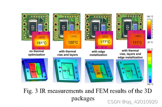
不同封装设计的实验和模拟结果令人印象深刻,具有热优化PCB设计的3D封装可以比传统封装多消耗50%的功率[图3]
图8显示了在组件功耗为48 W时水冷和3 W时不水冷的PCB堆栈的表面温度。水冷后,表面温度从约61°C降至仅31°C。部件温度由部件中间的传感器测量(图7)。在约85℃的温度下,展台内的测量值几乎相同。水冷降低了封装温度。PCB封装可以消耗大约15倍的功率
图9显示了电气部件的功率和部件温度之间的依赖关系。温度由3D封装内部功能层中心的PT100测量(图7)。在大约150毫升/分钟的水流中,48瓦时的温升不超过60 K。
introduction
开发了一种用于射流电气应用的新3D封装技术[3]。焊接环技术使封装的气密性达到8巴。一个优点是将电函数与流体分布函数相结合。
通过这种组合,3D PCB封装技术实现了更高的集成度和小型化。3D PCB封装的主要应用是集成低功耗应用的可堆叠功能层(图1)[5]。

高功率应用的最大挑战是将封装中心的热量耗散到环境中[1]。可堆叠大功率PCB层与射流冷却的结合包括两个进步的技术发展。首先,在非常紧凑的高集成度封装中,倒装芯片、带有处理器的COB或具有短垂直连接路径的内存芯片的可堆叠功能层。第二,利用流体总线和热交换器解决封装内部的冷却问题
The biggest challenge for high-power applications is to dissipate the heat from the center of the package to the environment [1]. The combination of stackable high-power PCB layers with fluidic cooling comprises two progress technology developments. First, the stackable function layers for flip-chips, COBs with processors or memory chips with short vertical connection path in a very compact high-integration package. And second, the solution of the cooling in the inside of the package with fluidic bus and thermal management [1] to dissipate the heat to the environment.
Thermal management in 3D-Packages
三维封装中的热管理目标是从堆栈中的第一个模块到其他模块到环境的电源的最佳散热。热通道(通过热层边缘金属化的热通道)将热量引导至模块。
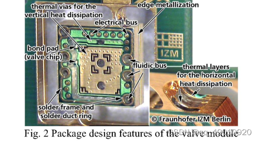
为了找出哪种热优化特性将产生哪种热效应,研究不同的PCB设计很重要。用于阀门模块的PCB设计如图2所示。
所研究的3D封装具有相同的功能特征,带有气流通道,但没有阀芯片。因此,我们使用了1 W电阻器和温度传感器。测量结果与阀门模块包相似。
Goal is the optimal heat dissipation of the source of the power from the first module in the stack over the other modules to the environment. The thermal paths (thermal via-thermal layeri edge metallization) lead the heat thru the module.
To find out which thermal optimization feature will have which thermal effect, it was important to investigate different PCB designs. The PCB design used for the valve module is shown in Fig. 2.
The investigated 3D packages have the same functional features, with air flow channels, but have no valve chips. Therefore we used a 1 W resistor and a temperature sensor. The measurement results are similar to the package of the valve modules.
不同封装设计的实验和模拟结果令人印象深刻,具有热优化PCB设计的3D封装可以比传统封装多消耗50%的功率[图3]。由于热层和通孔直接接触,它们可以非常有效地将热量从内部散发到环境[1]。
The 3D-PCB-Package with water cooling
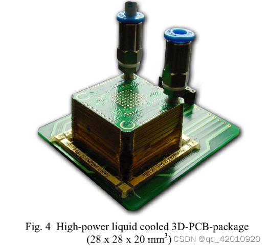
High-power resistors and one PT1 00 temperature sensor are integrated in the function layer to simulate the high-power function (Fig. 4). 48 W of power have to be dissipated in 2 of these function layers with a temperature control in the center of the 3D-package.
功能层中集成了带有水冷高功率电阻器和一个PT1 00温度传感器的3D PCB封装,以模拟高功率功能(图4)。48瓦的功率必须消耗在其中两个功能层中,温度控制位于3D封装的中心。
Thermal Management in the 3D-PCB-Packages with water cooling
目标是在通向环境或水道的热路径上实现电堆内部电源的最佳散热。
图6显示了3D PCB封装中热路径的设计概念
具有散热的PCB设计必须具有从封装内部到边缘的最佳金属化路径。为了确保这一点,我们的封装具有用于垂直散热的热通孔和用于水平散热的金属化层。所有热通孔和热层均处于短路状态,并与PCB布局的电气功能绝缘。焊接环连接来自一个PCB的热网络,以均匀分布热量。
图7中的红外测量显示了封装表面和功率元件的独特温度。

A PCB design with heat dissipation must have optimal metallization paths from the inside to the edges of the package. To ensure this, our packages have thermal vias for the vertical heat dissipation and metallization layers for the horizontal heat dissipation. All thermal vias and layers are in a short circuit and insulated with the electrical functions of the PCB-layout. The solder ring connects the thermal network from one PCB for a uniformly distributed the heat.
The infra-red measurements in Fig. 7 show a very unique temperature of the package surface and the power components.
This method of thermal management strategies (Fig. 6) dissipates the heat from the components to the environment or to the water.
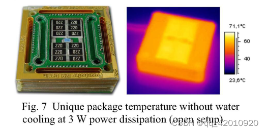
图8显示了在组件功耗为48 W时水冷和3 W时不水冷的PCB堆栈的表面温度。水冷后,表面温度从约61°C降至仅31°C。部件温度由部件中间的传感器测量(图7)。在约85℃的温度下,展台内的测量值几乎相同。水冷降低了封装温度。PCB封装可以消耗大约15倍的功率
Fig. 8 shows the surface temperatures of the PCB stack with water cooling at 48 W and without water cooling at 3 W of power dissipation in the Components. The surface temperature decrease from about 61 °C to only 31 °C with water cooling. The component temperatures are measured by the tsensor in the middle of the components (Fig. 7). And is in booth measurements nearly the same at about 85 'C. The water cooling is reducing the package temperature. And the PCB package can dissipate about 15 times more power
图9显示了电气部件的功率和部件温度之间的依赖关系。温度由3D封装内部功能层中心的PT100测量(图7)。在大约150毫升/分钟的水流中,48瓦时的温升不超过60 K。
所有PCB层的厚度和标准生产规格相同。所有PCB层都可以在同一PCB板上生产。通过这种方式,可以非常经济高效地生产该技术的演示器。在进一步的技术开发中,可以更改这些规范以降低热阻并增加热交换。

Fig. 9 shows the dependency between the power of the electrical components and the temperature of the components. The temperature is measured by PT100 in the center of the function layer inside the 3D-package (Fig. 7). The temperature rise at 48 W does not exceed 60 K at a flow of the water of about 150 ml/min.
All PCB-layers have the same thickness and standard production specifications. All PCB-layers can be produced on the same PCB-panel. In this way, the demonstrator for this technology could be produced very cost-efficiently. In further technology developments, it is possible to change these specifications to reduce the thermal resistance and to increase the thermal heat exchange.
Spacer stacking technology
具有或不具有流体结构的低功率3D封装和高功率封装可以使用相同的技术进行堆叠[3]。一个PCB层的顶面将用锡膏印刷,这是一个非常常见的SMD工艺步骤。放置电气元件后,所有PCB层将在对齐工具中连接。层之间的焊膏在气相焊接机中熔化。
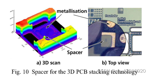
垫片防止焊球和焊料流体结构受到过强压缩。垫片技术使用与焊球厚度相同的油漆或清漆(图10)。这种清漆由PCB生产商制造,不可逆地印刷在PCB的底面上。'
Low-power 3D-packages and high-power packages with or without fluidic structures can be stacked with the same technology [3]. The top-side of one PCB layer will be printed with solder paste, which is a very common SMD process step. After the place of the electrical components, all PCB-layers will be joint in the alignment tool. The solder paste between the layers is melting in a vapor-phase soldering machine.
The spacer prevents the solder balls and solder fluidic structures from too strong compression. The spacer technology uses a lacquer, or varnish with the same thickness as the solder balls (Fig. 10). This varnish is made by the PCB producer and is printed irreversibly onto the bottom surface of the PCB.
间隔技术的另一种可能性是使用薄FR4多层材料。这种材料的厚度为100μm,很容易用铣床加工。在堆叠过程中,垫片将放置在PCB层之间。
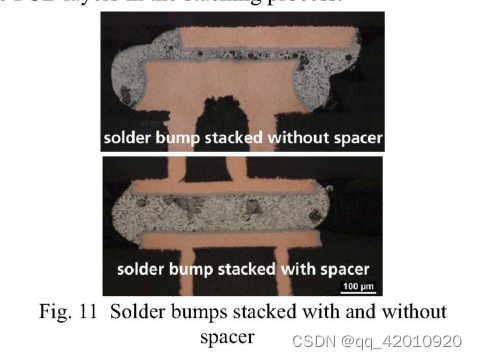
3DPCB封装堆叠技术的垫片产生了非常独特的焊球和焊环。图10显示了带和不带焊接环的3D封装。用于PCB堆叠的垫片技术具有发明专利。
nother possibility for the spacer technology is to use thin FR4 multilayer material. That material is 100 pim thick and can easily be structured by a milling machine. The spacer will be placed between the PCB layers in the stacking process.
The spacer for the stacking technology of 3DPCB-packages leads to very unique solder balls and solder rings. Fig. 10 shows 3D-packages with and without solder rings. The spacer technology for PCB stacking has an invention patent.
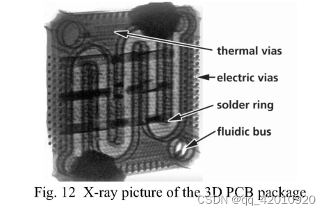
图12显示了包装的x射线照片。它显示了焊环、许多热过孔和电气总线。焊接环是闭合的,以确保水不会与PCB材料接触。水道本身镀有铜和薄金层(见图6)。这对于PCB材料中没有湿度影响的可靠封装非常重要。
Fig. 12 shows a x-ray picture of the package. It shows the solder rings, the many thermal vias and the electrical bus. The solder rings are closed to ensure that the water will not get in contact with the PCB material. The water channels themselves are metallised with copper and a thin gold layer (see Fig. 6). That is important for a reliable package with no humidity effects in the PCB material.
conclusion:
对于可重复的过程,带间隔的PCB堆叠技术是一种非常简单的解决方案。不需要复杂的额外材料或工艺步骤。电子或流体/电子PCB的堆叠技术与标准SMD技术兼容。
水冷电子产品的重要性正在上升。由于高功率3D封装中的水循环是功率元件散热的解决方案,因此在水冷3D封装中有2、4或更多功率元件层的新产品是可能的。
如果电气元件与水进行更好的热交换,则可以优化3D PCB封装。这可以通过微通道冷却器、更薄的功能PCB层或组件与3D封装之间的导热填充材料来实现。
微通道冷却器效率很高,但压降很大。这意味着需要一个具有这些扩展规格的泵。
水泵可能非常膨胀。开发一种需要非常膨胀的水泵的廉价水冷机组是没有意义的。水道的横截面非常大(2 x 1.5 mm2)。这意味着我们需要一个高流速的泵来进行令人满意的热交换。这些泵体积小,价格便宜。这就是市场上已有的水冷设备概念
The PCB stacking technology with spacer is a very simple solution for a reproducible process. No complex extra materials or process steps are necessary. The stacking technology of electrical or fluidic/electrical PCBs is compatible with the standard SMD technology.
The importance of water-cooled electronics is rising. New products are possible with 2, 4 or more power component layers in a water-cooled 3Dpackage, because the water circulation in a highpower 3D-package is the solution to dissipate the heat of the power component.
The 3D-PCB-package can be optimized if the electrical components get a better heat exchange with the water. This can be realized with micro channel coolers, thinner function PCB layers, or thermally conductive underfiller material between the components and the 3D-package.
Micro channel coolers can be very efficient but there is a big pressure drop. And that means that there a pump with these expansive specifications is needed.
Water pumps can be very expansive. It makes no sense to develop a cheap water cooling package which needs very expansive water pumps. The cross section of the water channels is very large (2 x 1.5 mm2). That means that we need a pump with a high flow rate to have a satisfying heat exchange. These pumps are small and inexpensive. That is the concept of water cooling equipment already available on the market


 1187
1187


 被折叠的 条评论
为什么被折叠?
被折叠的 条评论
为什么被折叠?
 到【灌水乐园】发言


