


目录
(一)initialize SysTick without interrupts --- check COUNTFLAG
(二)initialize SysTick with interrupts --- SysTick_Handler()
一、registers
MSP432的System Timer滴答定时器是一个24位的自减计数器。该定时器包含3个寄存器,见下表:
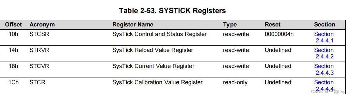
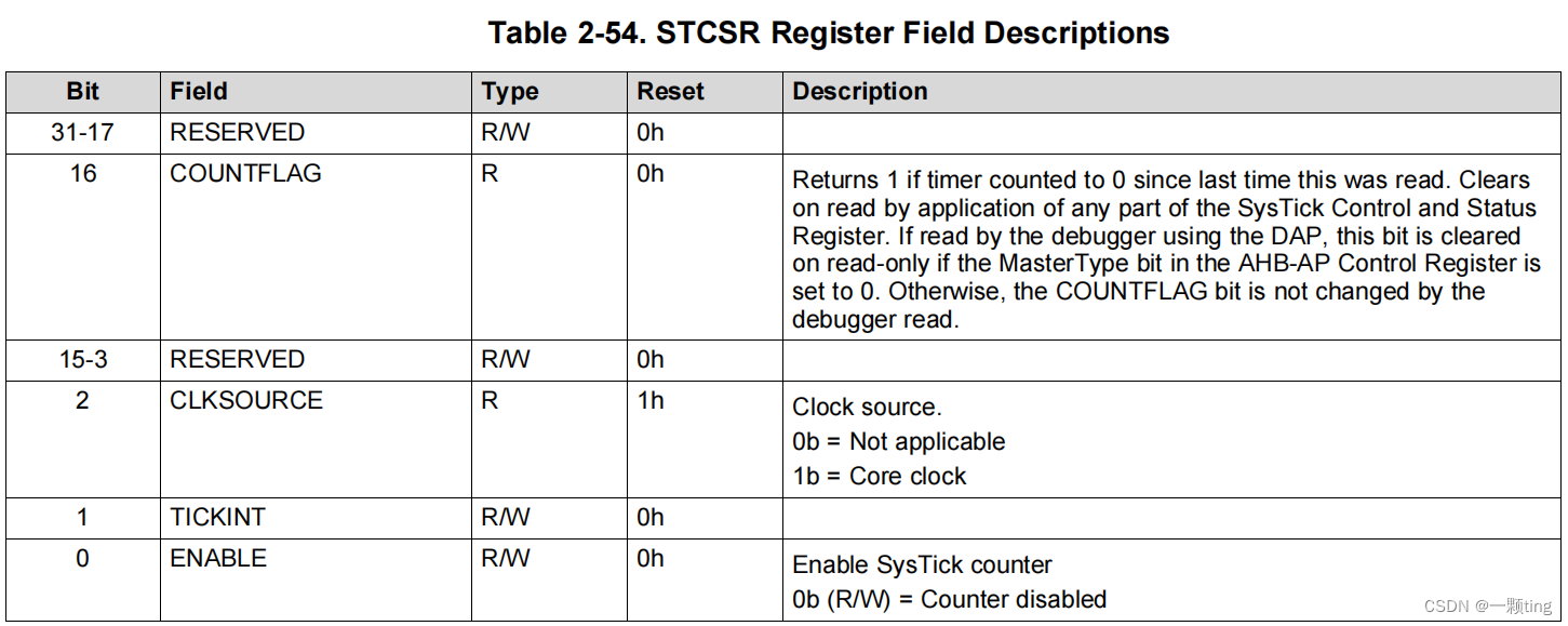
STCSR(Systick Control and Status Register):用于配置其时钟,启用计数器,启用SysTick中断,并确定计数器状态。
STRVR(SysTick Reload Value Register):使用SysTick重新加载值寄存器指定要加载的起始值。当计数器达到0时,输入当前值寄存器。它可以是介于1和0x00FFFFFF之间的任何值。起始值为0是可能的,且但没有作用,因为从1计数到0时,SysTick中断和COUNTFLAG标志位被激活。

STCVR(SysTick Current Value Register):提供计数器的current 计数值。

二、SysTick_Init
复位时,未定义SysTick计数器重新加载和当前值;初始化SysTick计数器步骤为:
1.设置STRVR寄存器中的重装载值reload;
2.向STCVR寄存器中写入任意值,以清除该寄存器;
3.根据所需配置STCSR寄存器
(一)initialize SysTick without interrupts --- check COUNTFLAG
// assumes 48 MHz bus clock

void SysTick_Init(void){
  SysTick->LOAD = 0x00FFFFFF;           // maximum reload value
  SysTick->CTRL = 0x00000005;           // bus clock, enable SysTick with no interrupts
  SysTick->VAL = 0;          // any write to CVR clears it and COUNTFLAG in CSR
}

// method : set Reload Value Register, clear Current Value Register, poll COUNTFLAG in Control and Status Register
void SysTick_Wait(uint32_t delay){
  if(delay <= 1){
    // without this step:
    // if delay == 0, this function will wait 0x00FFFFFF cycles
    // if delay == 1, this function will never return (because COUNTFLAG is set on 1->0 transition)
    return;                   // do nothing; at least 1 cycle has already passed anyway
  }
  SysTick->LOAD = (delay - 1);// count down to zero
  SysTick->VAL = 0;          // any write to CVR clears it and COUNTFLAG in CSR
  while(( SysTick->CTRL&0x00010000) == 0){};//check COUNTFLAG

// Time delay using busy wait.
void SysTick_Wait10ms(uint32_t delay){
  uint32_t i;
  for(i=0; i<delay; i++){
    SysTick_Wait(480000);  // wait 10ms (assumes 48 MHz clock)
  }
}
(二)initialize SysTick with interrupts --- SysTick_Handler()
// **************SysTick_Init*********************
// Initialize SysTick periodic interrupts
// Input: interrupt period
//           Units of period are in bus clock period
//           Maximum is 2^24-1
//           Minimum is determined by execution time of the ISR
// Input: priority 0 (high) to 7 (low)
// Output: none
void SysTick_Init(uint32_t period, uint32_t priority){
  SysTick->CTRL = 0;              // 1) disable SysTick during setup
  SysTick->LOAD = period - 1;     // 2) reload value sets period
  SysTick->VAL = 0;               // 3) any write to current clears it
  SCB->SHP[11] = priority<<5;     // set priority into top 3 bits of 8-bit register
  SysTick->CTRL = 0x00000007;     // 4) enable SysTick with core clock and interrupts
}

void SysTick_Handler(void){

}


 433
433


 被折叠的 条评论
为什么被折叠?
被折叠的 条评论
为什么被折叠?
 到【灌水乐园】发言


