


FPGA ODDR原语
一、原语例化内容
//      ODDR     : In order to incorporate this function into the design,
//     Verilog   : the following instance declaration needs to be placed
//    instance   : in the body of the design code.  The instance name
//   declaration : (ODDR_inst) and/or the port declarations within the
//      code     : parenthesis may be changed to properly reference and
//               : connect this function to the design.  Delete or comment
//               : out inputs/outs that are not necessary.

//  <-----Cut code below this line---->

   // ODDR: Output Double Data Rate Output Register with Set, Reset
   //       and Clock Enable.
   //       Artix-7
   // Xilinx HDL Language Template, version 2019.2

   ODDR #(
      .DDR_CLK_EDGE("OPPOSITE_EDGE"), // "OPPOSITE_EDGE" or "SAME_EDGE"
      .INIT(1'b0),    // Initial value of Q: 1'b0 or 1'b1
      .SRTYPE("SYNC") // Set/Reset type: "SYNC" or "ASYNC"
   ) ODDR_inst (
      .Q(Q),   // 1-bit DDR output
      .C(C),   // 1-bit clock input
      .CE(CE), // 1-bit clock enable input
      .D1(D1), // 1-bit data input (positive edge)
      .D2(D2), // 1-bit data input (negative edge)
      .R(R),   // 1-bit reset
      .S(S)    // 1-bit set
   );

   // End of ODDR_inst instantiation
二、参数含义
表中给出了各个参数的含义和默认值。
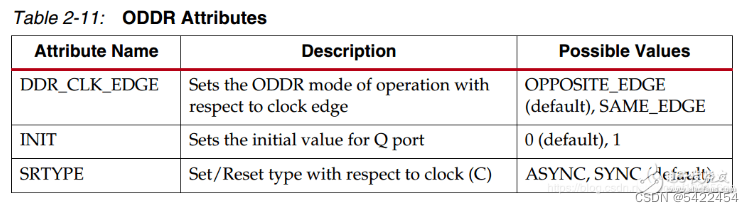
DDR_CLK_EDGE:可选择OPPOSITE_EDGE或者SAME_EDGE。
1)OPPOSITE_EDGE
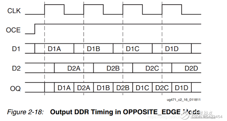
这种模式下我认为是在clk上升沿采D1的数据,下降沿采D2数据,数据会延迟一点时间输出。
仿真如下图

2)SAME_EDGE模式
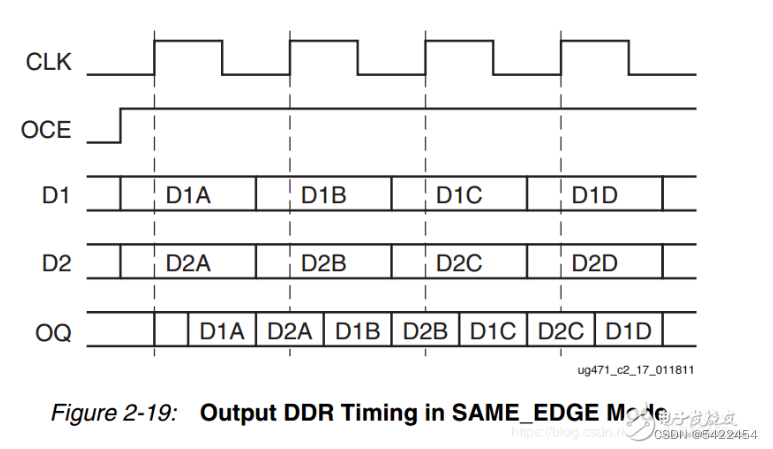
这种模式下是在上升沿采集D1 D2的数据,然后在上升沿延迟一点时间输出D1,下降沿延迟一段时间输出D2。
仿真如下图
三、应用
Oserdes、FPGA源同步系统的设计,用ODDR使得随路时钟和数据输出是严格同步的,保证相位严格对齐关系。
看到fpga官方PLL例程中将时钟D1赋值为1,D2赋值为0,参数设置成默认值,得到一个具有和输入时钟有固定延时的时钟。(在100MHz时,这个延时是100ps)

四、注意
1.Set和Reset不能同时置位。
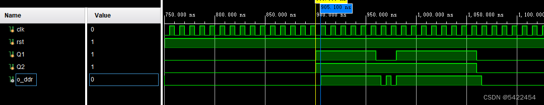
2.ODDR原语的复位需要约12个clock,第一次输入的数据可能会有问题。


 623
623


 被折叠的 条评论
为什么被折叠?
被折叠的 条评论
为什么被折叠?
 到【灌水乐园】发言


