


一、STM32F103的IIC接口实现
1.任务要求
(1)显示自己的学号和姓名;
(2)显示AHT20的温度和湿度;
(3)上下或左右的滑动显示长字符,比如“Hello,欢迎来到重庆交通大学物联网205实训室!”或者歌词、诗词。(最好使用硬件刷屏模式)
2.代码提取
野火官网下载工程代码
3.打开工程

4.修改代码
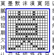
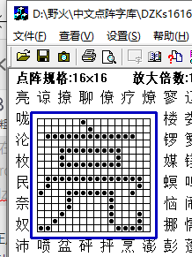
(1)生成字模
生成一个16*16的字模
原理

在点阵库里把自己需要的找到,写出对应的数据
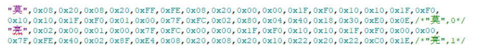
例如:
对应数据:
{0x20,0x01,0x20,0x11,0x20,0x11,0x27,0xD2,0xF5,0x52,0x25,0x54,0x25,0x58,0x25,0x70,0x25,0x58,0x25,0x54,0xF5,0x52,0x27,0xD2},
{0x20,0x11,0x20,0x11,0x20,0x01,0x00,0x00},/“莫”,0/
{0x00,0x21,0x20,0xC1,0x20,0x82,0x2E,0x84,0x2A,0xB8,0x2A,0xA0,0xAA,0xA0,0x6A,0xA0,0x2A,0xA0,0x2A,0xA0,0x2A,0xBE,0x2E,0x81},
{0x20,0x81,0x20,0xA1,0x00,0xC7,0x00,0x00},/“亮”,1/
(2)添加代码
打开文件

将自己需要的字符添加进去
这样就OK了。
二、温湿度显示
1.相关函数
/*****************************************************************************
							显示温湿度
******************************************************************************/
void Temp_Hum(float temp, float hum)
{
	char data1[4],data2[4];
	sprintf(data1, "%.1f", temp);

	GUI_DrawLine(0, 10, WIDTH-1, 10,1);
	GUI_DrawLine(WIDTH/2-1,11,WIDTH/2-1,HEIGHT-1,1);
	GUI_DrawLine(WIDTH/2-1,10+(HEIGHT-10)/2-1,WIDTH-1,10+(HEIGHT-10)/2-1,1);
	GUI_ShowString(0,1,"2020-12-20",8,1);
	GUI_ShowString(78,1,"Sunday",8,1);
	GUI_ShowString(14,HEIGHT-1-10,"Cloudy",8,1);
	//温度
	GUI_ShowString(WIDTH/2-1+2,13,"TEMP",8,1);
	GUI_DrawCircle(WIDTH-1-19, 25, 1,2);
	GUI_ShowString(WIDTH-1-14,20,"C",16,1);
	GUI_ShowString(WIDTH/2-1+9,20,(u8 *)data1,16,1);

	//湿度
	GUI_ShowString(WIDTH/2-1+2,39,"HUM",8,1);
	GUI_DrawBMP(6,16,51,32, BMP5, 1);
	sprintf(data2, "%.1f", hum);
	GUI_ShowString(WIDTH/2-1+9,46,(u8 *)data2,16,1);
	GUI_ShowString(WIDTH-1-14,46,"%",16,1);
}
main.c
#include "stm32f10x.h"
#include "bsp_usart.h"
#include "delay.h"
#include "bsp_aht20.h"
#include "bsp_led.h"
#include "gui.h"
#include "oled.h"
#include "test.h"

extern u32 flag;//标志是否开启延迟
int main(void)
{
	u32 CT_data[2]={0};
    volatile float  hum=0,temp=0;
	u32 i=1;
	u32 num = 0;//记录AHT20采集次数
	USART_Config();			//USART1初始化
	LED_GPIO_Config();		//LED端口初始化
    delay_init();	    	//延时函数初始化
    temphum_init();         //初始化温湿度传感器
	OLED_Init();			         //初始化OLED
	OLED_Clear(0);             //清屏(全黑)
	while(1)
	{
		flag = i;
		/* 采集3次温湿度  */
		if(i<4)
		{
			AHT20_Read_CTdata(CT_data);       //不经过CRC校验,直接读取AHT20的温度和湿度数据
			hum = CT_data[0]*100*10/1024/1024;  //计算得到湿度值(放大了10倍)
			temp = CT_data[1]*200*10/1024/1024-500;//计算得到温度值(放大了10倍)

			printf("湿度:%.1f%%\r\n",(hum/10));
			printf("温度:%.1f度\r\n",(temp/10));
			printf("\r\n");
			Temp_Hum(temp/10, hum/10);
			num++;
			green_led_on;
			delay_ms(1000);
			green_led_off;
			delay_ms(1000);
		}

		/* 显示个人简介 */
		if(i==4){
			OLED_Clear(0);
			Display_introduction();
			delay_ms(1000);
		}

		/*  显示个人座右铭*/
		if(i==5)
		{
			OLED_Clear(0);
			Display_motto();
			delay_ms(1000);
			OLED_Clear(0);
			i = 0;
			num=0;
		}
		if(num == 3)
		{
			num = 0;
			i = 3;
		}

		i++;
		printf("i=%d,num=%d\r\n",i,num);
	 }
}
OLED屏滚动指令
参考链接
SSD1306-0.96寸oled屏-滚动指令介绍
效果展示


 896
896


 被折叠的 条评论
为什么被折叠?
被折叠的 条评论
为什么被折叠?
 到【灌水乐园】发言


