


构建一个没有输入和一个输出常数1的输出的电路
定义了一个名为top_module的模块,该模块具有一个输出端口one,并将该端口的值赋值为1。
output wire one;:这定义了一个名为one的输出端口。output关键字表示这是一个输出端口,而wire表示这是一个线性的端口类型。这意味着one是一个用于输出信号的线性端口。assign one = 1;:这一行使用assign关键字将输出端口one赋值为1。这意味着无论何时引用one端口,它都将输出1。
创建一个具有一个输入和一个输出的模块,其行为类似于电路上的连线。
input in0:定义一个名为in0的输入端口。输入端口可以接收一个单独的信号,通常是一个位(1位)信号。output out1:定义一个名为out1的输出端口。assign out1 = in0;:连线部分,将in0值分配给out1。这意味着out1端口的值将始终与in0端口的值相同。
创建一个具有 2个输入和 3个输出的模块,使用线连接的方式:a->z,b->x,b->y
input wire a, b:这定义了两个输入端口,分别命名为a和b。它们都被声明为线性(wire)端口类型,表示它们用于输入信号,并且信号可以被赋值和连线。output wire x, y, z:这定义了三个输出端口,分别命名为x、y和z。它们也被声明为线性端口类型,表示它们用于输出信号。assign z = a;:这一行使用assign关键字将输入端口a的值赋值给输出端口z。assign x = b;:这一行使用assign关键字将输入端口b的值赋值给输出端口x。assign y = b;:这一行使用assign关键字将输入端口b的值赋值给输出端口y。
输出输入信号的值的相反的值
input in:这定义了一个名为in的输入端口。它表示该模块将接收一个单一的位(1位)输入信号,该信号可以是0或1。output out:这定义了一个名为out的输出端口。这个输出端口将被用来输出与输入端口in相反的信号。assign out = ~in;:这一行使用assign关键字来实现逻辑赋值。它将输出端口out赋值为输入端口in的逻辑反值(取反)。也就是说,如果输入信号in为0,那么输出信号out将为1,反之亦然。
创建实现 AND 门的模块,输入有三个wire,将三个信号(a b c)进行与操作,请思考在实际电路需要几个与门?
input a, b, c:这定义了三个输入端口,分别命名为a、b和c。它们表示该模块接收三个输入信号,每个信号可以是0或1。output d:这定义了一个名为d的输出端口。这个输出端口将用于输出逻辑与(AND)操作的结果。assign d = a & b & c;:这一行使用assign关键字将输出端口d赋值为输入端口a、b和c的逻辑与操作的结果。这意味着只有当a、b和c都为1时,d端口才会输出1;否则,d端口将输出0
input a, b, c:这定义了三个输入端口,分别命名为a、b和c。它们表示该模块接收三个输入信号,每个信号可以是0或1.output d:这定义了一个名为d的输出端口。这个输出端口将用于输出逻辑与(AND)操作的结果.assign d = a & b & c:这一行使用assign关键字将输出端口d赋值为输入端口a、b和c的逻辑与操作的结果。这意味着只有当a、b和c都为1时,d端口才会输出1;否则,d端口将输出0.
创建实现 OR和NOR 的模块,NOR 门是输出反相的 OR 门。
c 是 nor输出,d是or输出
assign c = ~d,d = a | b:这一行包含了两个赋值语句。
首先,c端口被赋值为~d,表示c的值等于d的逻辑反值(取反)。
其次,d端口被赋值为a|b,表示d的值等于输入端口a和b的逻辑或操作的结果。
-
~d表示将d的值取反,即如果d为 1,则c为 0,反之亦然。 -
a | b表示将输入信号a和b进行逻辑或操作,即如果a或b中有至少一个为 1,那么d为 1;如果两者都为 0,那么d为 0。
创建一个实现 XOR 门的模块
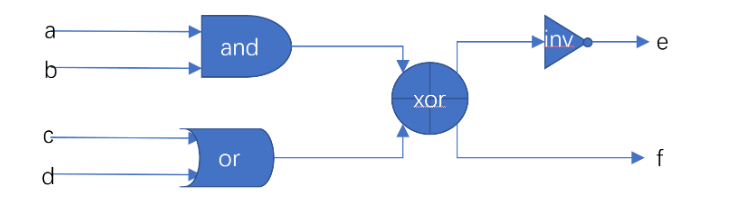
写出如图的rtl逻辑,限制使用最多四次assign
多位信号:构建一个具有一个3位输入in的信号[2:0],将其分成三个独立的输出a b c(从2到0)
module top_module(input [2:0] in, output a, b, c);:这是模块的定义开始,模块名为top_module,并在括号中列出了模块的输入和输出端口。(1)input [2:0] in:这定义了一个名为in的输入端口,它是一个3位宽的信号。[2:0]表示这个信号可以包含3个比特,即可以表示0到7之间的整数值。因此,in可以取8种不同的二进制组合,从000到111 (2)output a, b, c:这定义了三个输出端口,分别命名为a、b和c。这些输出端口将用于输出in端口的不同比特值。assign {a, b, c} = in;:这一行使用assign关键字,将输入端口in的值拆分成三个部分,并分别赋值给输出端口a、b和c。使用{}括号表示一个向量的赋值,其中a接收in的最低位,b接收in的中间位,c接收in的最高位。
一个16位信号in包含四个四位数[3:0]a[3:0]b[3:0]c[3:0]d,将它们顺序倒置为dcba输出,输出out
wire [3:0] a, b, c, d;:这定义了四个中间的线性信号端口,分别命名为a、b、c和d。每个中间端口都是4位宽的线性信号。assign {a, b, c, d} = in;:这一行使用assign关键字,将输入端口in的值拆分成四个部分,并分别赋值给中间端口a、b、c和d。使用{}括号表示一个向量的赋值,其中a接收in的低4位,b接收in的接下来的4位,以此类推。assign out = {d, c, b, a};:这一行将中间端口d、c、b和a的值重新组合成一个16位宽的向量,并赋值给输出端口out。这个操作实际上是对输入信号in的反转,即输出信号out的最低位是输入信号in的最高位,
现有一个模块,输入信号为[2:0]a和[2:0]b,请输出信号的按位或[2:0]c和或信号d
或:| 按位或;|| 逻辑或;
将一个五输入的信号分别进行的每一位进行: 全部按位与;全部按位或;全部按位异或
input [4:0] in:这是一个5位宽的输入端口,用于接收一个5位宽的数据。[4:0]表示索引范围从4到0,因此in是一个包含5个位的向量。
然后,使用assign语句为这些输出端口分配值:
assign out_and = &in[4:0];:这将out_and设置为输入向量in中所有位的按位与操作的结果。换句话说,out_and将等于in[4] & in[3] & in[2] & in[1] & in[0]。assign out_or = |in[4:0];:这将out_or设置为输入向量in中所有位的按位或操作的结果。换句话说,out_or将等于in[4] | in[3] | in[2] | in[1] | in[0]。assign out_xor = ^in[4:0];:这将out_xor设置为输入向量in中所有位的按位异或操作的结果。换句话说,out_xor将等于in[4] ^ in[3] ^ in[2] ^ in[1] ^ in[0]。
将6个输入信号串联转为四个信号输出,输入信号为[4:0] a[4:0] b[4:0]c [4:0]d [4:0]e [4:0]f,末尾增加一个宽度为两位的3,形成32位长度后,按照从前到后的顺序输出[7:0]w [7:0]x [7:0]y [7:0]z
{a,b,c,d,e,f,2'b11}是拼接操作。
输入一个16位的信号in,将其从低位到高位输出(即反转顺序输出)为out
给定四个无符号数字,找到最大值。不使用if进行判断,尽量少使用语句的情况下完成。
三元操作符,同C语言。
给定五个1bit信号(a、b、c、d 和 e),生成两种25位的数据: 一种是将信号复制五次后连接起来aaaaabbbbb...,一种是将信号连接起来复制五次成为abcdeabcde... 。比较两个25位信号,如果两个信号的同样位置的位相等,则输出1。
使用assign语句为这两个wire赋值:
assign out1 = {{5{a}},{5{b}},{5{c}},{5{d}},{5{e}}};
-
{{5{a}},{5{b}},{5{c}},{5{d}},{5{e}}}是一个拼接操作,它将每个输入端口a、b、c、d和e分别复制5次,然后将它们连接成一个25位宽的向量。因此,out1包含了输入端口的值,每个值都重复了5次。
assign out2 = {5{a,b,c,d,e}};
-
{5{a,b,c,d,e}}也是一个拼接操作,它将输入端口a、b、c、d和e的值组合成一个5位宽的向量,然后将这个向量重复5次,形成一个25位宽的向量。因此,out2包含了输入端口的值,每个值都重复了5次。
输入5个4bit信号,根据sel的值选出对应的信号,对应关系为:0~a 1~b 2~c 3~d 4~e 其他~置零
在模块的主体中,使用 always 块来创建一个组合逻辑,该逻辑会根据 sel 的值选择要输出的输入端口的值。具体地说,它使用 case 语句来根据 sel 的不同值进行选择:


 543
543

 被折叠的 条评论
为什么被折叠?
被折叠的 条评论
为什么被折叠?
 到【灌水乐园】发言


