


 文章详细描述了如何利用SC8701和SC8703实现Buck和Boost电路,设置了Vout为13.2V和不同的Vin值。电路中涉及MOS驱动、Schottky二极管和反馈机制,强调了反馈样本电路应靠近输出,以消除振荡。还提到了LT3741数据手册作为参考。
1. Set condition
#1, Use SC8701 and SC8703 realize Buck and Boost circuit;
#2, Vout 13.2V with feedback setting
#3, Vin set 8V for boost, Vin set 20V for buck
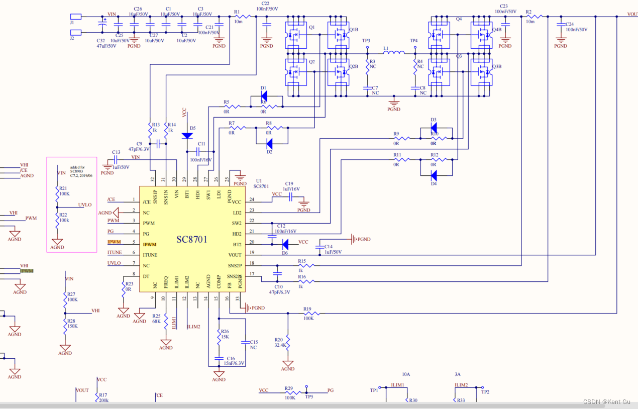
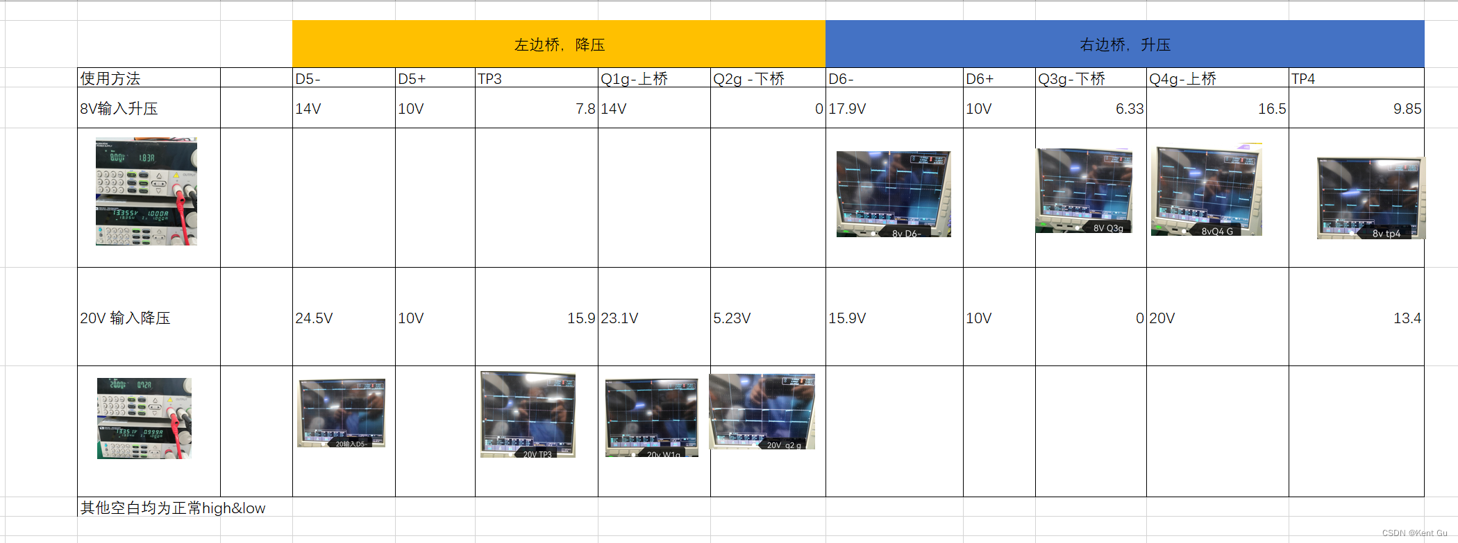
2. Buck function signal(Vin with 20V in)
2.1, Q4 always on(make output path), and Q3 always off(cut off ground path
2.2, Q4.G/BT2 signal is about CW 20V
2.3, Vcc =10V, SW2 is 0/13.2V square wave, and schotty diode and C realize about 20V voltage for MOS drive.
2.4, Q1 & Q2 realize buck circuit.
2.5, TP4 is 13.2V square wave output voltage
2.6. TP3 is CW wave
3. Boost function signal(Vin 8V)
3.1, Q1 always on(make Vin path), and Q2 always off(cut off ground path
2.2, Q1.G/BT2 signal is about 15V
2.3, Vcc =10V, SW1 is 8V DC wave, and schotty diode and C realize about 15V voltage for MOS drive.
2.4, Q4 & Q1 realize boost circuit.
2.5, TP3/SW1 is CW 8V
2.6, TP6 is square wave
So Feedback sample circuit shoudl be close to output, and feedback with C for ripple removent.
The below is LT3741 datasheet.


 736
736

 被折叠的 条评论
为什么被折叠?
被折叠的 条评论
为什么被折叠?
 到【灌水乐园】发言


