


这次来分享分享AD835的电路图:

电路很简单,也就几个元件,AD835这个芯片引脚少,使用方便,就外接几个元件就可以,下面的两个是防反接二极管,还有上电指示灯,不过如果考虑功耗的话不用像我这样用两个LED,板子三个接口分别是乘法器的两个输入端以及一个输出端,实现的是频谱的搬移。
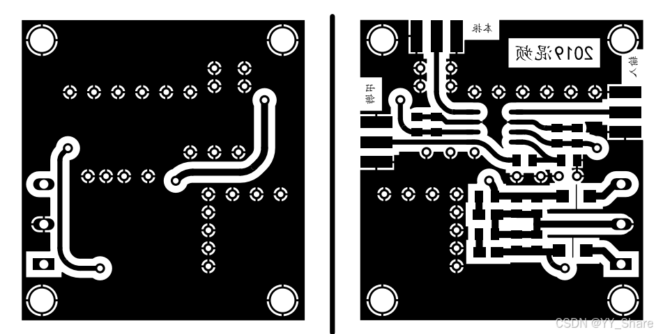
下面是PCB:


很明显这是2019年做的板子。
经过测试,是能够正常使用的。
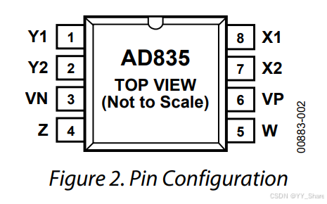
下面是芯片规格书说明
FEATURES Simple:
basic function is W = XY + Z
Complete: minimal external components required
Very fast: Settles to 0.1% of full scale (FS) in 20 ns
DC-coupled voltage output simplifies use
High differential input impedance X, Y, and Z inputs
Low multiplier noise: 50 nV/√Hz
FEATURESSimple:基本功能是W=XY+Z完整:所需的最小外部组件非常快:在20ns直流耦合电压输出中达到满量程(FS)的0.1%,简化了使用高差分输入阻抗X, Y和Z输入低乘法器噪声:50 nV/VHz
APPLICATIONS
Very fast multiplication, division, squaring Wideband modulation and demodulation Phase detection and measurement Sinusoidal frequency doubling Video gain control and keying Voltage-controlled amplifiers and filters
应用:非常快速的乘法,除法,平方,宽带调制和解调,相位检测和测量,正弦倍频,视频增益控制和键控,压控放大器和滤波器
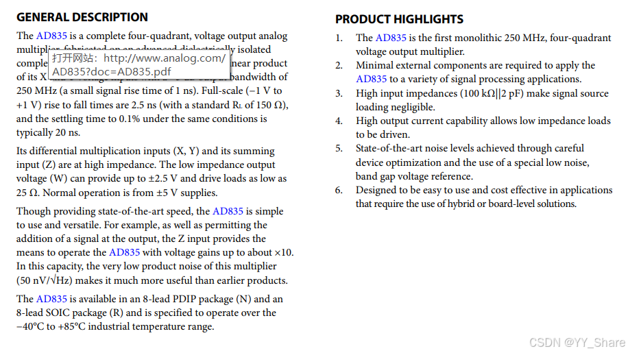
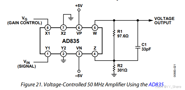
Table 4. Pin Function Descriptions
Pin No. Mnemonic Description
1 Y1 Noninverting Y Multiplicand Input 2 Y2 Inverting Y Multiplicand Input 3 VN Negative Supply Voltage 4 Z Summing Input 5 W Product 6 VP Positive Supply Voltage 7 X2 Inverting X Multiplicand Input 8 X1 Noninverting X Multiplicand Input
芯片引脚:
THEORY OF OPERATION
The AD835 is a four-quadrant, voltage output analog multiplier, fabricated on an advanced dielectrically isolated complementary bipolar process. In its basic mode, it provides the linear product of its X and Y voltage inputs. In this mode, the −3 dB output voltage bandwidth is 250 MHz (with small signal rise time of 1 ns). Full-scale (−1 V to +1 V) rise to fall times are 2.5 ns (with a standard RL of 150 Ω), and the settling time to 0.1% under the same conditions is typically 20 ns. As in earlier multipliers from Analog Devices a unique summing feature is provided at the Z input. As well as providing independent ground references for the input and the output and enhanced versatility, this feature allows the AD835 to operate with voltage gain. Its X-, Y-, and Z-input voltages are all nominally ±1 V FS, with an overrange of at least 20%. The inputs are fully differential at high impedance (100 kΩ||2 pF) and provide a 70 dB CMRR (f ≤ 1 MHz). The low impedance output is capable of driving loads as small as 25 Ω. The peak output can be as large as ±2.2 V minimum for RL = 150 Ω, or ±2.0 V minimum into RL = 50 Ω. The AD835 has much lower noise than the AD534 or AD734, making it attractive in low level, signal processing applications, for example, as a wideband gain control element or modulator.
BASIC THEORY
The multiplier is based on a classic form, having a translinear core, supported by three (X, Y, and Z) linearized voltage-to-current converters, and the load driving output amplifier. The scaling voltage (the denominator U in the equations) is provided by a band gap reference of novel design, optimized for ultralow noise. Figure 19 shows the functional block diagram. In general terms, the AD835 provides the function
( )( ) Z U YYXX W + −− = 2121 (1) where the variables W, U, X, Y, and Z are all voltages. Connected as a simple multiplier, with X = X1 − X2, Y = Y1 − Y2, and Z = 0 and with a scale factor adjustment (see Figure 19) that sets U = 1 V, the output can be expressed as W = XY (2)
00883-025
X1 X2 X = X1 – X2 Z INPUT Y = Y1 – Y2
AD835
W OUTPUT Y1 Y2 XY XY + Z X1 + +
Figure 19. Functional Block Diagram
Simplified representations of this sort, where all signals are presumed expressed in V, are used throughout this data sheet to avoid the needless use of less intuitive subscripted variables (such as, VX1). All variables as being normalized to 1 V. For example, the input X can either be stated as being in the −1 V to +1 V range or simply –1 to +1. The latter representation is found to facilitate the development of new functions using the AD835. The explicit inclusion of the denominator, U, is also less helpful, as in the case of the AD835, if it is not an electrical input variable.
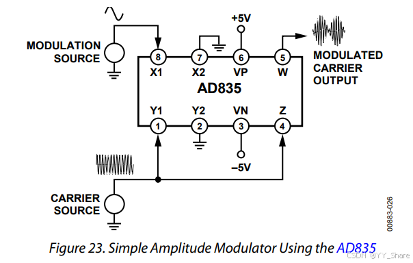
SCALING ADJUSTMENT
The basic value of U in Equation 1 is nominally 1.05 V. Figure 20, which shows the basic multiplier connections, also shows how the effective value of U can be adjusted to have any lower voltage (usually 1 V) through the use of a resistive divider between W (Pin 5) and Z (Pin 4). Using the general resistor values shown, Equation 1can be rewritten as
kW ( )Zk '1 U XY W −++= (3) where Z' is distinguished from the signal Z at Pin 4. It follows that
( ) ' 1 Z Uk XY W + − = (4) In this way, the effective value of U can be modified to
U’ = (1 − k)U (5) without altering the scaling of the Z' input, which is expected because the only ground reference for the output is through the Z' input. Therefore, to set U' to 1 V, remembering that the basic value of U is 1.05 V, R1 must have a nominal value of 20 × R2. The values shown allow U to be adjusted through the nominal range of 0.95 V to 1.05 V. That is, R2 provides a 5% gain adjustment. In many applications, the exact gain of the multiplier may not be very important; in which case, this network may be omitted entirely, or R2 fixed at 100 Ω.
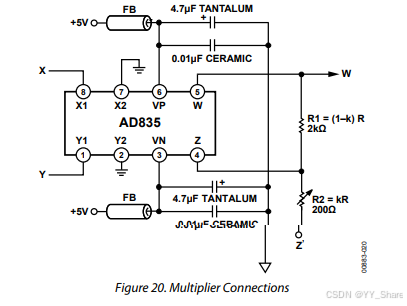
00883-020
+ + R1 = (1–k) R 2kΩ R2 = kR 200Ω Z’
FB +5V
AD835
4.7µF TANTALUM 0.01µF CERAMIC 0.01µF CERAMIC 4.7µF TANTALUM
1 2 3 4 8
X W Y X2 VP W Y1 X1 Y2 VN Z
7 6 5
FB +5V
Figure 20. Multiplier Connections


 1111
1111

 被折叠的 条评论
为什么被折叠?
被折叠的 条评论
为什么被折叠?
 到【灌水乐园】发言


