


 本文介绍了两种读取XILINXFPGADNA的方法,一种是通过JTAG接口,另一种是使用DNA_PORTE2原语。重点展示了使用Verilog状态机配合DNA_PORTE2原语的代码实现,经过仿真和硬件验证,证明代码可以成功读取并输出DNA号。此外,还提到了DNA值在不同FPGA系列中的位宽差异。
读取XILINX FPGA DNA有两种方法:
1、通过JTAG可直接查看FPGA的DNA号;此方法网上有很多教程,按下不表。但此种方法只能看到FPGA的DNA号,并不能将DNA号被上层读取。
2、通过DNA_PORTE2原语读取DNA号;
   DNA_PORTE2 #(
      .SIM_DNA_VALUE(96'h000000000000000000000000)  // Specifies a sample 96-bit DNA value for simulation
   )
   DNA_PORTE2_inst (
      .DOUT(DOUT),   // 1-bit output: DNA output data
      .CLK(CLK),     // 1-bit input: Clock input
      .DIN(DIN),     // 1-bit input: User data input pin
      .READ(READ),   // 1-bit input: Active-High load DNA, active-Low read input
      .SHIFT(SHIFT)  // 1-bit input: Active-High shift enable input
   );
详细解释可参考xilinx官方文档UG570。
此处给出通过该原语读取DNA号的verilog代码,该代码经过仿真和上版验证。
`timescale 1ns / 1ps
`define FPGA_DNA_BITS  96     //  96bits
//
// Company:
// Engineer: masl
//
// Create Date: 2023/07/15 09:43:44
// Design Name:
// Module Name: get_dna
// Project Name:
// Target Devices:
// Tool Versions:
// Description:
//
// Dependencies:
//
// Revision:
// Revision 0.01 - File Created
// Additional Comments:
//
//


module get_dna(
//global clock&reset
	input clk,
	input rst_n,
//user interface
	output reg [`FPGA_DNA_BITS-1:0] dna,
	output reg dan_value
);
	localparam IDLE   = 4'd0;
	localparam READ   = 4'd1;
	localparam SHIFT  = 4'd2;
	localparam END	  = 4'd3;

	reg [3:0] current_state;
	reg [3:0] next_state;

	reg [7:0] bit_cnt;
	reg read;
	reg shift;
	wire dout;
/*******************************************************************
                        State machine(1)
********************************************************************/
    always@(posedge clk or negedge rst_n)begin
        if(~rst_n)begin
            current_state <= IDLE;
        end
        else begin
            current_state <= next_state;
        end
    end

/*******************************************************************
                            State machine(2)
********************************************************************/
    always@(*)begin
        case(current_state)
            IDLE:   begin
						if(bit_cnt == 8'd9)
							next_state = READ;
						else
							next_state = IDLE;
                    end
    		READ:   begin
						if(bit_cnt == 8'd4)
							next_state = SHIFT;
						else
							next_state = READ;
    				end
    		SHIFT : begin
						if(bit_cnt == `FPGA_DNA_BITS)
							next_state = END;
						else
							next_state = SHIFT;
					end
    		END:  	begin
						next_state = END;
    				end
            default : next_state = IDLE;
    	endcase
    end

/*******************************************************************
                         bit_cnt
********************************************************************/
    always@(posedge clk or negedge rst_n)begin
        if(~rst_n)begin
            bit_cnt <= 8'd0;
        end
        else begin
            case(current_state)
    			IDLE :	begin
    						if(bit_cnt != 8'd9)
    							bit_cnt <= bit_cnt + 1'b1;
    						else
    							bit_cnt <= 8'd0;
    					end
    			READ :	begin
    						if(bit_cnt != 8'd4)
    							bit_cnt <= bit_cnt + 1'b1;
    						else
    							bit_cnt <= 8'd0;
    					end
    			SHIFT :	begin
    						if(bit_cnt != `FPGA_DNA_BITS)
    							bit_cnt <= bit_cnt + 1'b1;
    						else
    							bit_cnt <= 8'd0;
    					end
                default:  bit_cnt <= 8'd0;
            endcase
        end
    end

/*******************************************************************
                         read
********************************************************************/
    always@(posedge clk or negedge rst_n)begin
        if(~rst_n)begin
            read <= 1'b0;
        end
        else begin
    		if(current_state == READ)
    			read <= 1'b1;
    		else
    			read <= 1'b0;
        end
    end

/*******************************************************************
                         dan_value
********************************************************************/
    always@(posedge clk or negedge rst_n)begin
        if(~rst_n)begin
            dan_value <= 1'b0;
        end
        else begin
            case(current_state)
    			SHIFT :	begin
    						if(bit_cnt == `FPGA_DNA_BITS)
    							dan_value <= 1'b1;
    						else
    							dan_value <= 1'b0;
    					end
                default :	dan_value <= 1'b0;
            endcase
        end
    end

/*******************************************************************
                         dna  shift
********************************************************************/
    always@(posedge clk or negedge rst_n)begin
        if(~rst_n)begin
            dna <= 'd0;
    		shift <= 1'b0;
        end
        else begin
            if(current_state == SHIFT)begin
    			dna <= {dna[`FPGA_DNA_BITS-1:1],dout};
    			shift <= 1'b1;
    		end
    		else begin
    			dna <= dna;
    			shift <= 1'b0;
    		end
        end
    end

    DNA_PORTE2 #(
		.SIM_DNA_VALUE(96'h0000_0000_0000_0000_0000_1234)  // Specifies a sample 96-bit DNA value for simulation
	)
	DNA_PORTE2_inst (
		.DOUT(dout),   // 1-bit output: DNA output data
		.CLK(clk),     // 1-bit input: Clock input
		.DIN(1'b1),    // 1-bit input: User data input pin
		.READ(read),   // 1-bit input: Active-High load DNA, active-Low read input
		.SHIFT(shift)  // 1-bit input: Active-High shift enable input
	);

endmodule
仿真结果如下: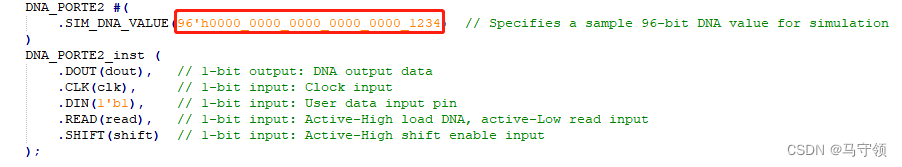
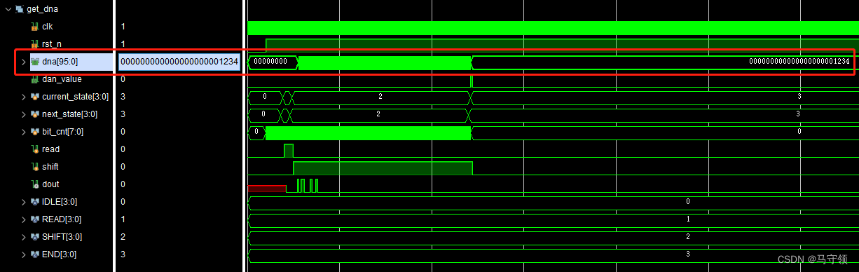
注意:1、实际上板时将96'h0000_0000_0000_0000_0000_1234改为96'h0000_0000_0000_0000_0000_0000即可;
2、Ultrascale系列的DNA号为96bit,其他系列有的DNA号是有57bit的,这时应使用下面的原语:
   DNA_PORT #(
      .SIM_DNA_VALUE(57'h000000000000000)  // Specifies a sample 57-bit DNA value for simulation
   )
   DNA_PORT_inst (
      .DOUT(DOUT),   // 1-bit output: DNA output data.
      .CLK(CLK),     // 1-bit input: Clock input.
      .DIN(DIN),     // 1-bit input: User data input pin.
      .READ(READ),   // 1-bit input: Active high load DNA, active low read input.
      .SHIFT(SHIFT)  // 1-bit input: Active high shift enable input.
   );
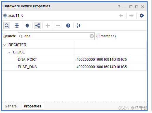
实际上版验证:
通过Jtag查看FPGA的DNA号如下图所示:
工程中添加上面get_dna.v代码,读到的dna号结果如下图所示: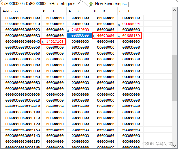
get_dna.v代码得到的DNA号与Jtag查看FPGA的DNA号一致,证实代码可行。


 被折叠的 条评论
为什么被折叠?
被折叠的 条评论
为什么被折叠?
 到【灌水乐园】发言


