


textbook:Computer Organization and Architecture 10th - William Stallings
useful tool:
十进制转二进制转补码:
https://www.99cankao.com/numbers/twos-complement.php
补码加法运算:
https://www.easycalculation.com/2s-complement-addition.php
补码转十进制
https://www.exploringbinary.com/twos-complement-converter/
floating point:
见程序
boolean func化简:
https://www.boolean-algebra.com/
https://www.emathhelp.net/zh-hans/calculators/discrete-mathematics/boolean-algebra-calculator/?f=x%28%7Ey%7Ez+%2B+yz%29
(第二个好用一点)
真值表转func:(带kmap)
http://tma.main.jp/logic/index_en.html
根据真值表画图:logisim
syllabus

评分:
Grades
Grade A (A+, A, A-), 15% - 20%
Grade A and Grade B (B+, B, 😎, ~ 60%

lab
汇编
参考这里
数据变量声明:.data
代码段声明:.text
数据声明格式:
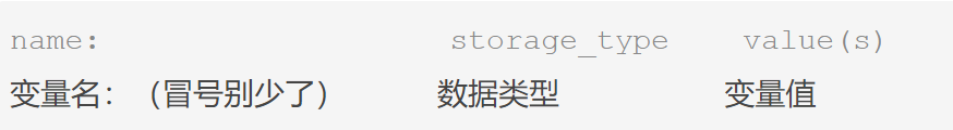
例:var1: .word 3;
array1: .space 12(定义一个 12字节 长度的数组 array1, 容纳 3个整型)
load/store 读取写入
w:word
b:byte
a:address
读取load:
lw register_destination, RAM_source
从内存中 复制 RAM_source 的内容到 对应的寄存器中
lw指loadword,同理可以换成lb(load byte)
写入store:
sw register_source, RAM_destination
将指定寄存器中的数据 写入 到指定的内存中
sw是store word

Indirect and Based Addressing立即与间接寻址
直接寻址
la $t0, var1
将var1的地址赋给寄存器t0
间接寻址
lw $t2, ($t0)
将地址为寄存器t0中的内容的内容赋给寄存器t2
sw $t2, ($t0)
将寄存器t2的内容赋给地址为t0内容的内存
偏移量:
sw $t2, -4($t0)
将寄存器t2的内容赋给地址为(t0内容-4)的内存
算数指令

控制流
branch分支ifelse
跳转(while,for,goto)

子程序调用
system call/IO
lab1
lec
lec1
computer=
os+CPU+RAM+**Graphics+Storage+Printers

cpu :

cpu-control unit:

cpu instruction cycle:fetch and execution
important registers
Program Counter (PC): stores the memory address of the next instruction (will increment after fetching an instruction)
Instruction Register (IR): stores the instruction currently being executed
Memory Address Register (MAR): stores the memory address from which data (also instructions) will be fetched to CPU
Memory Buffer Register (MBR): stores the data being transferred to and from the immediate access storage (like a buffer to store data temporarily)
CPU action in fetch:
know the instruction’s memory address (pc)
->instruction put in MAR, cpu fetch
->instruction put in MBR, loaded into IR
fetch 完成,pc到下一个
lec2 numberSystem & computer Arithmetic
10进制正整数转2进制:

10进制小数转2进制:(有时候达到不了确定值)


表示范围:

Arithmetic & Logic Unit (ALU)

补码:
10进制负整数:先用10进制正数表示,然后取其补码(1换0,0换1然后+1)
10进制负小数:floating point representation
bias=E+127
加减乘
加法检测overflow:
- 符号不同,不会出现;
- 符号相同,检测运算后的符号位和被运算符号位是否相同,如果不同则判定overflow
- 补码6位101101(-19)加补码6位111001(-7)得出来7位,去首1 100110(-26)未溢出
- 10011 + 10111
- 补码 101101 (-19) + 101001(-23)相加结果 1 010110 去掉第7位,010110,符号改变,有溢出(六位补码表示范围-32,31)
- 当补码加法两个数不一样长时,往左补0(1011+11=1011+1111)
减法:反向加法
乘法:

Use two operations “add” and “shift” to implement the addition
if bit in the multiplier is 0: just shift
if bit in the multiplier is 1: add and shift


注:因为Q每执行一次都要右移,空出的空间可以用来储存productA,所以储存空间从2n降到n
十进制转2进制
整数:

浮点数:

浮点数表示法

lec3 assembly language
MIPS

Register-based architecture:
cpu在register上进行操作:
operations can be divided into two categories:
(1) memory access (load and store data between memory and registers)
(2) ALU operations (operations between registers)
MIPS registers:


MIPS memory:

0xFFFFFF到0x800000是ROM和OS用的,;user program能用的地方呗分成三部分:
text,data,stack。
R-type instructions:


I-type instructions


J type instruction:

jump:

如何用instruction里的26bit表示32bit的地址?
1, 一个instruction有4byte,因此每个instruction的第一个byte是4的倍数,所以最后两个bit一定是00
2,跳转地址的前四位数和本地址(pc)的前四位数一样,我们不跳的太远

meaning of u
addu: overflow is ignored does not mean unsigned
add : overflow cause interrupt
一般用addu
multiple/division:
using lo and hi


lec4 MIPS Assembly Language
0/sign extend
ADDI, ADDIU are both use signed-extend.
ANDI, ORI, XORI both use zero-extend.
zero: constant must 非负数
operands
- shiftleft: unsigned and 不忽略有效数字
-
- shiftright: 补码表示
- logical: 补0
- arithmetic:补1
- noop: sll $0,$0, 0
- lx d, offset(b)
lec5 MIPS Assembly Language
jump
instruction cycle:

并不是到了j那一句就直接跳转的,要到下一句才行,换句话说jump后面的一个指令一定会被执行(所以设置成noop)

例,循环五次,addiu被执行5次。
(branch等跳转地址同理)
寄存器使用规范
-
$t0 - t9: subroutines can use without caution
-
$s0 - $s7: saved registers; subroutines should not use (if need to use it, save the value first and restore the value after use)
-
$a0 - $a3: contain arguments for the subroutine
-
$v0 - $v1: contain values returned from the subroutine
-
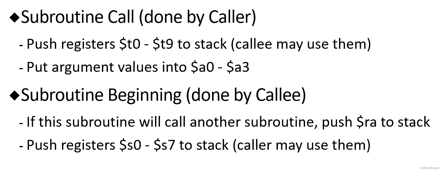
Recall: Caller should use $s0 - $s7, Callee should use $t0 - $t9
-
如果既是caller也是callee,用s0到s7,但要用stack存
-

lec6 digital logic1
boolean计算器
化简:
https://www.boolean-algebra.com/
真值表转func:
http://tma.main.jp/logic/index_en.html
boolean Algebra
n个变量有几个switch function:22n
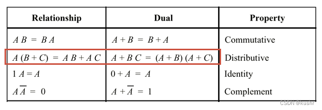
dual:
and变or,or变and,0,1互换(是/非不互换!)
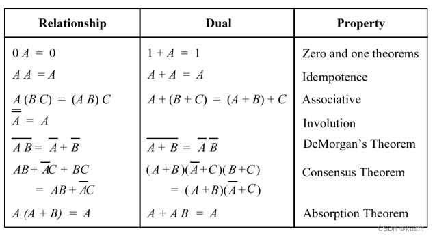
consensus Theorem:
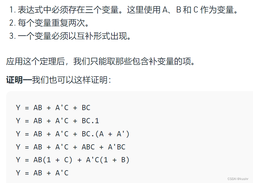
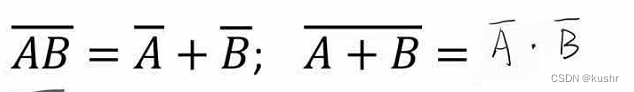
DeMoegan’s Theorem
用于消除and/or operation
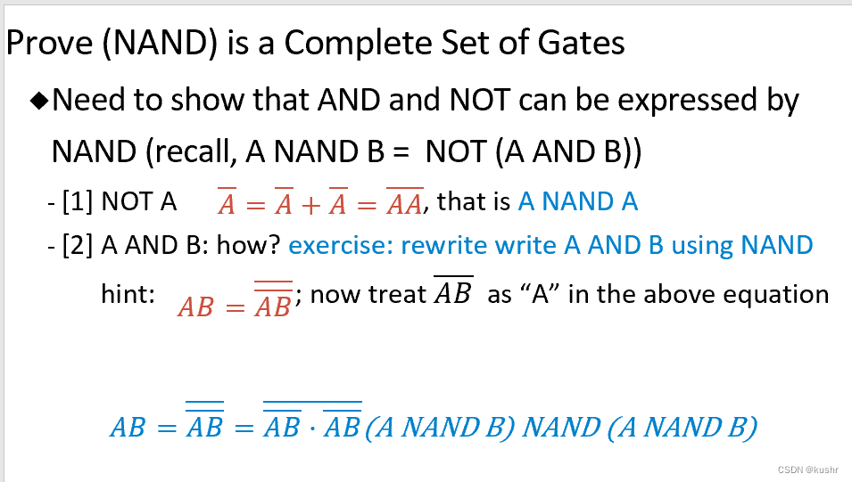
completeness of functionality
实现and,or,和not
(NAND)
证明:NAND
(NOR)
(OR,NOT)
(AND, NOT)
证明:用and和not表示or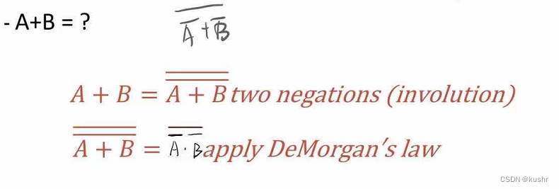
combinational logic
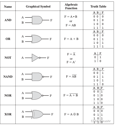
sop:乘积的和,easy to get(真值表)
lec7 digital logic2
simplification: 纯计算/kmap/Quine-McKluskey
Sequential Circuits
输出由输入和上一次输出决定
stable state:如果输入不变,则输出不变
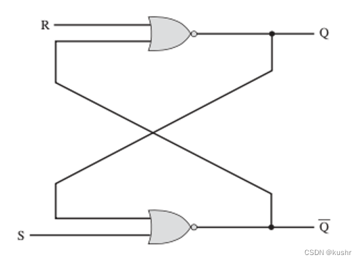
计算顺序:
以sr flip-flop为例,知道input sr和q,!q后,先用s和q计算非q,再用计算过的非q计算q
计算得出sr的characteristic table
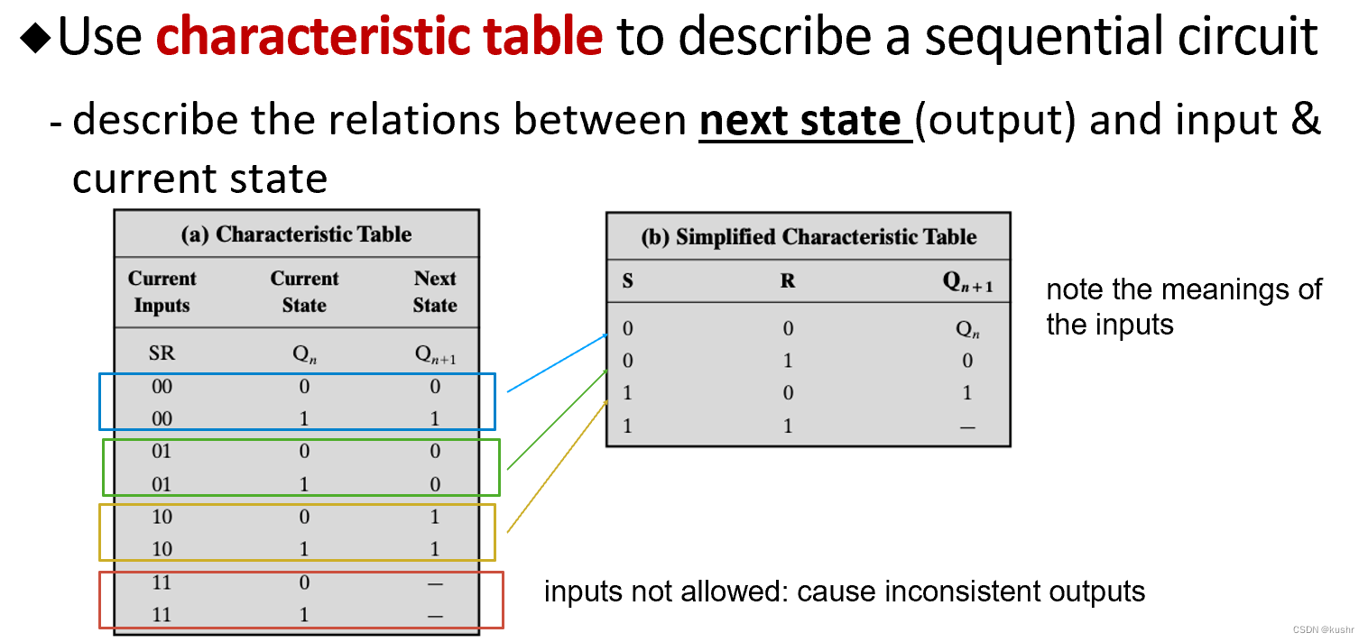
(s=1,r=1时q和q非数值相同,所以不能出现)
timing
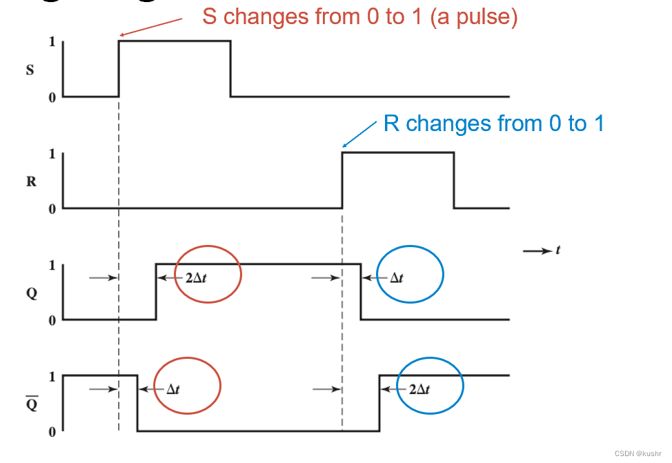
gate延时,可能会导致错误
在输入中用and连接一个clock:
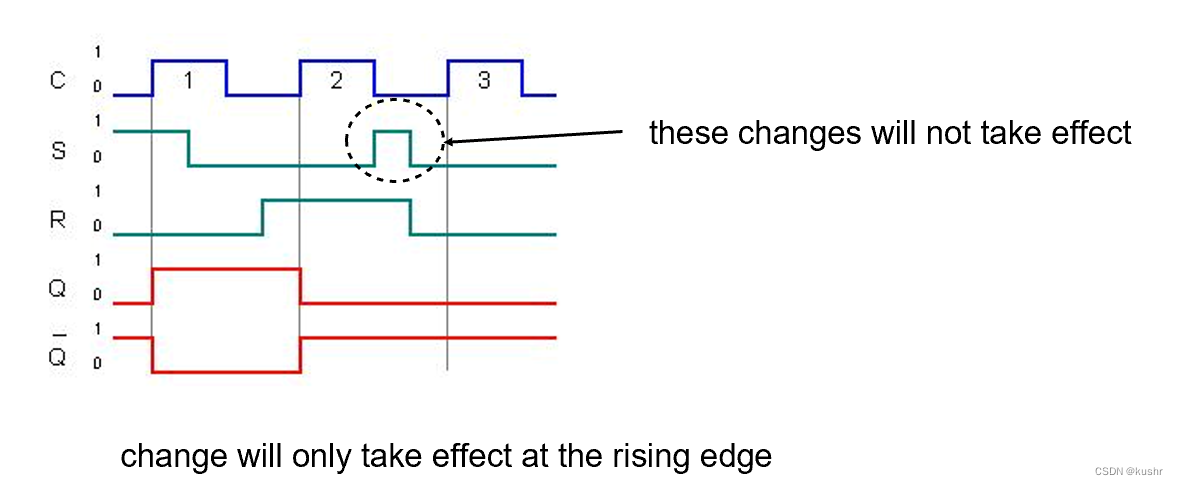
如果是positive edge triggered,则只有clock从0变1时改变才生效
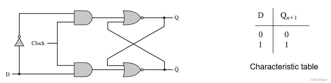
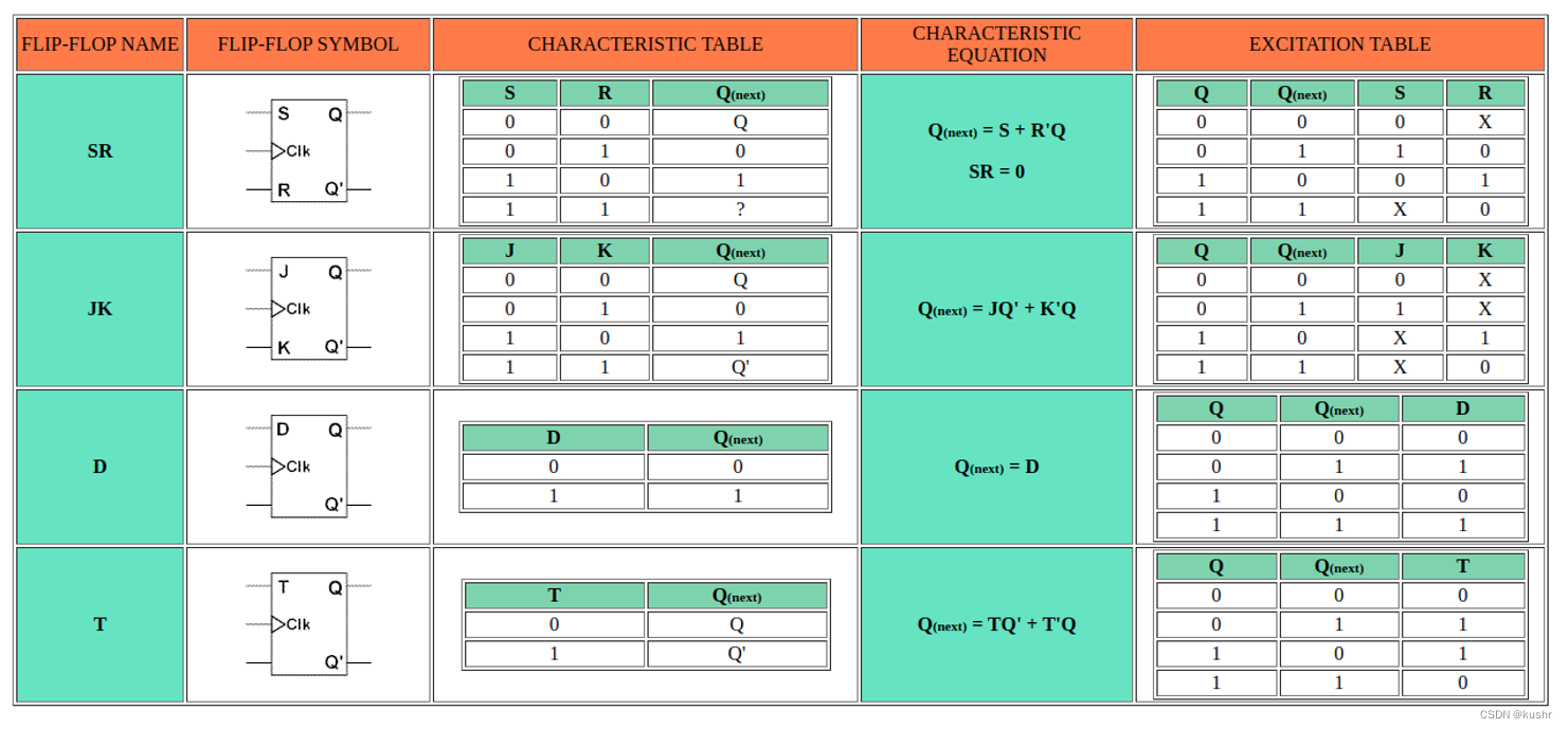
other ff
D-FF
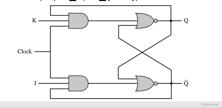
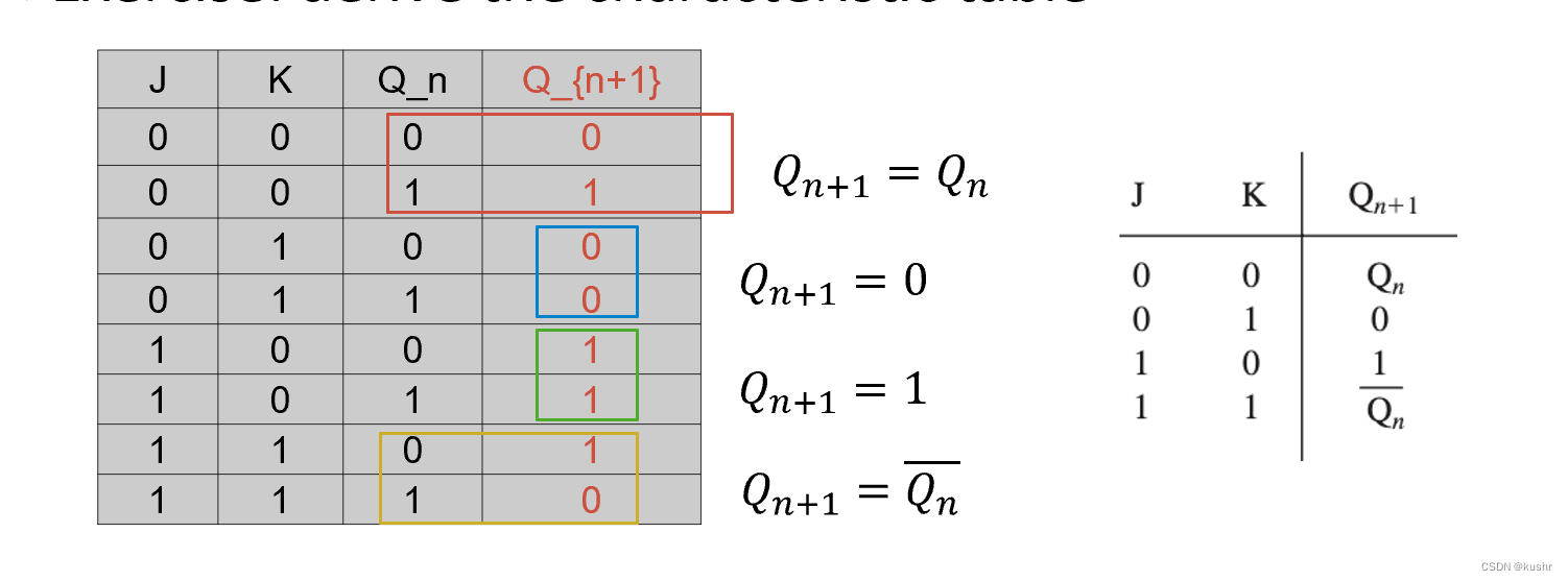
JK-FF
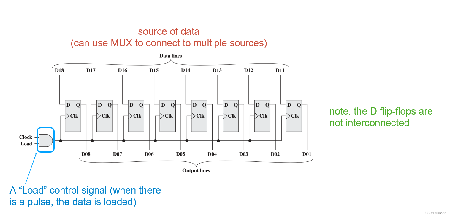
registers/counters
parallel register:同时改变输出
synchronous counter:states of flip-flops WILL change at the same time
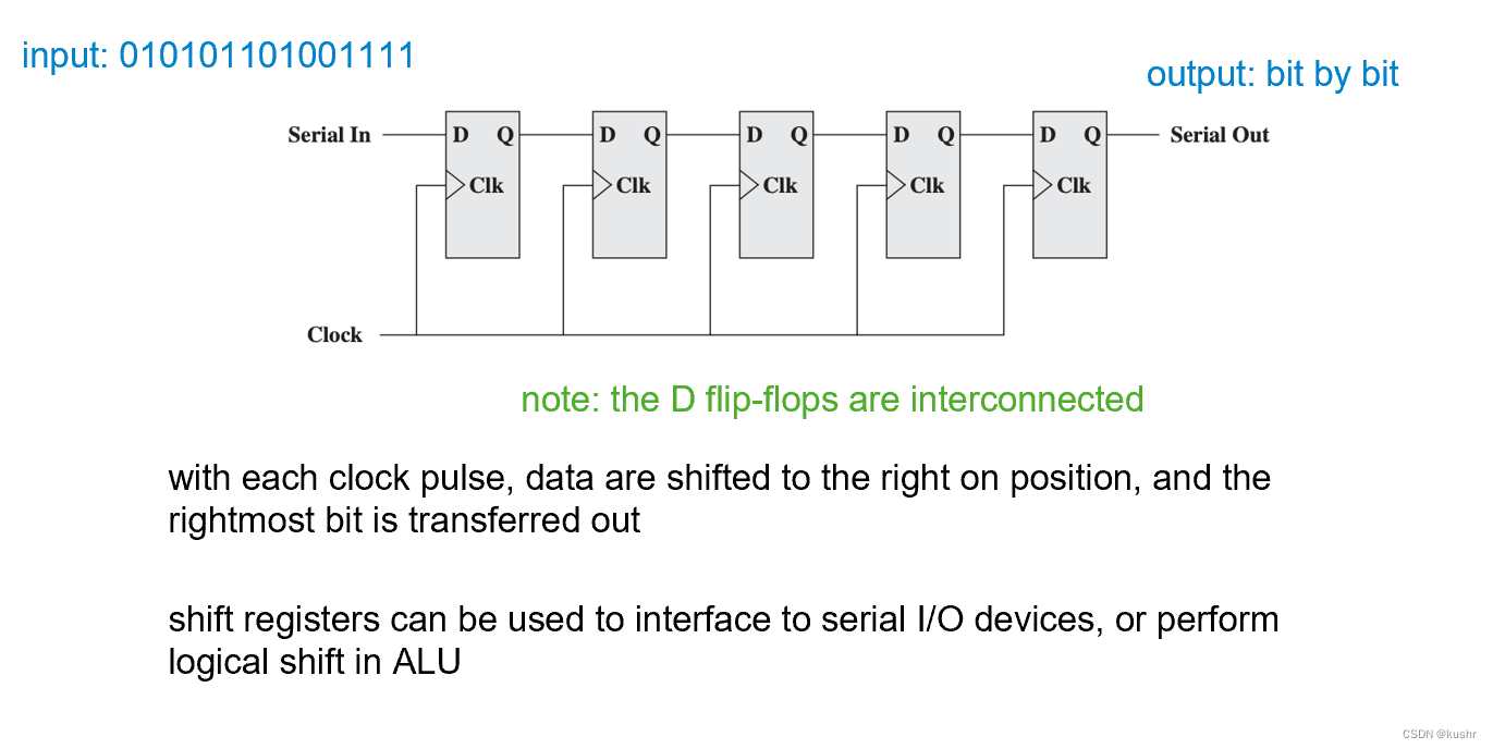
shift register: 依次改变输出:
asynchronous counter:states of flip-flops will NOT change at the same time
asynchronous :ripple counter
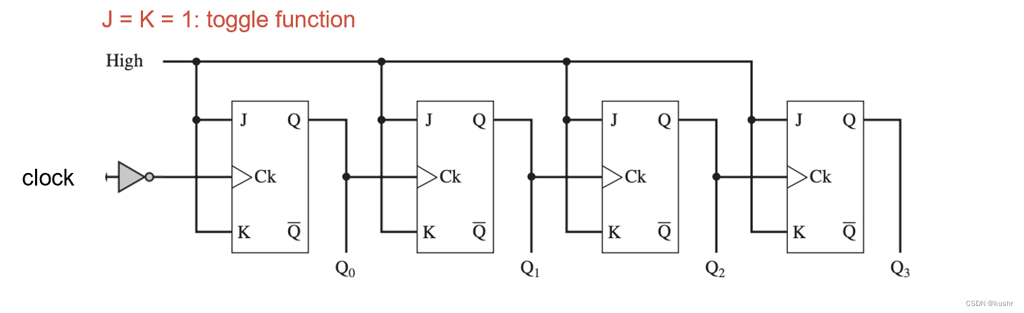
j=k=1(q=!q), 前一个ff的输出作为后一个ff的clock
synchronous counter
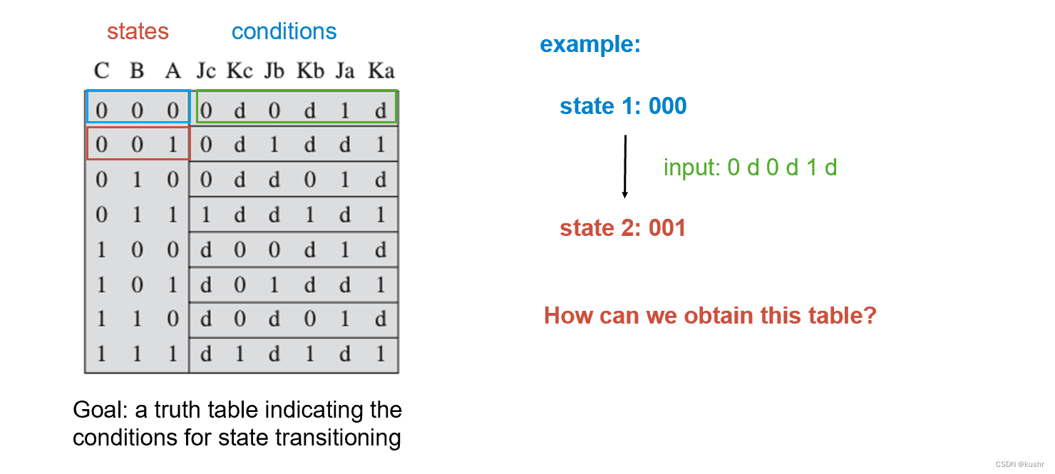
lec8 有限状态机(FSM)/顺序电路设计
FSM
Next state = external input + current state
External output = external input + current state
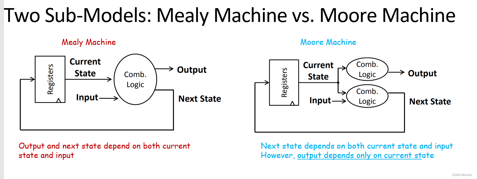
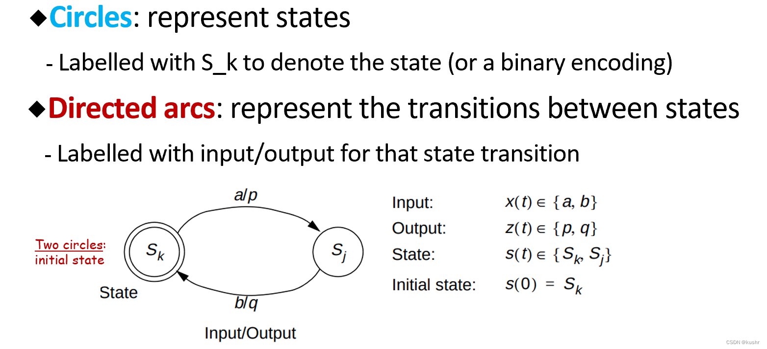
diagram to table:
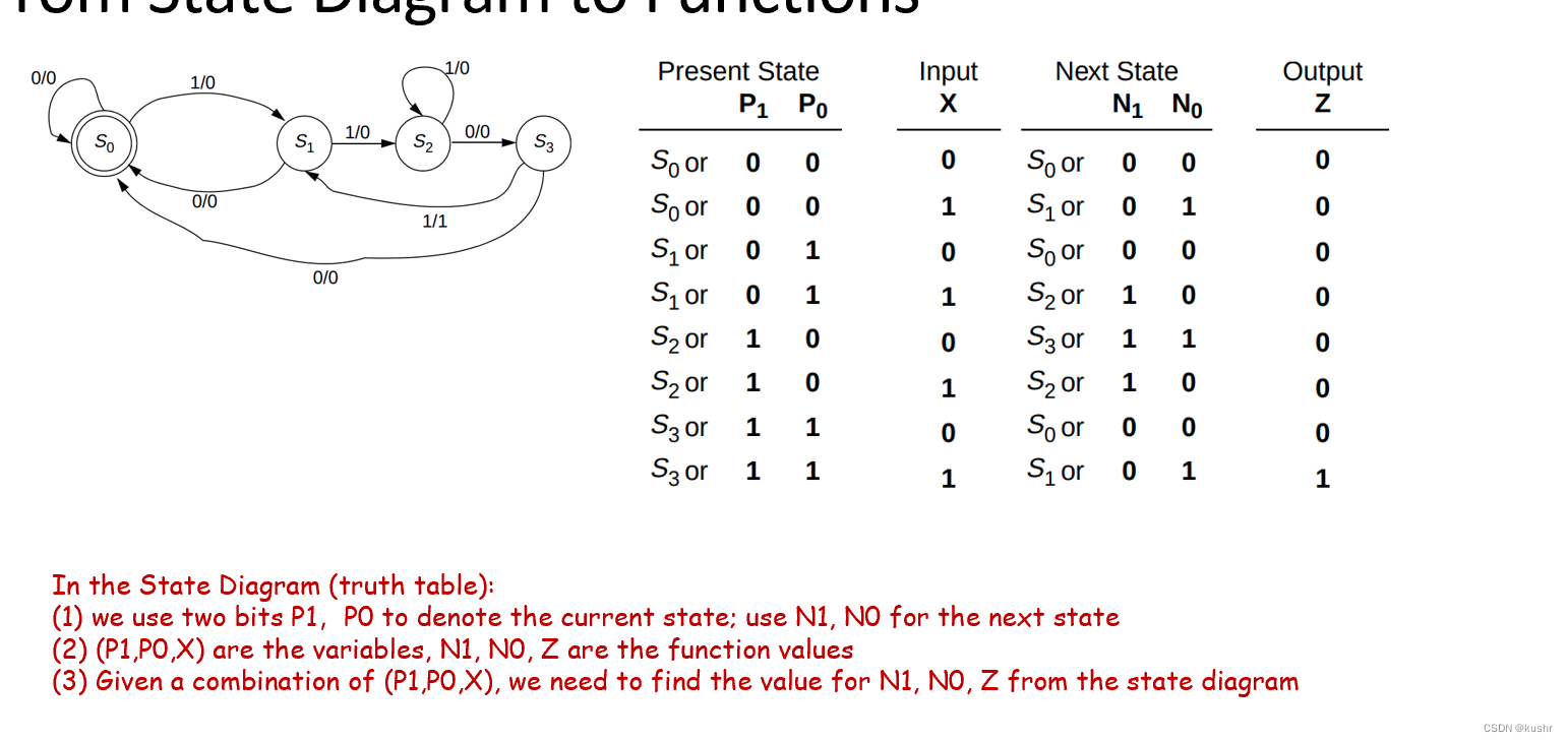
table to func:
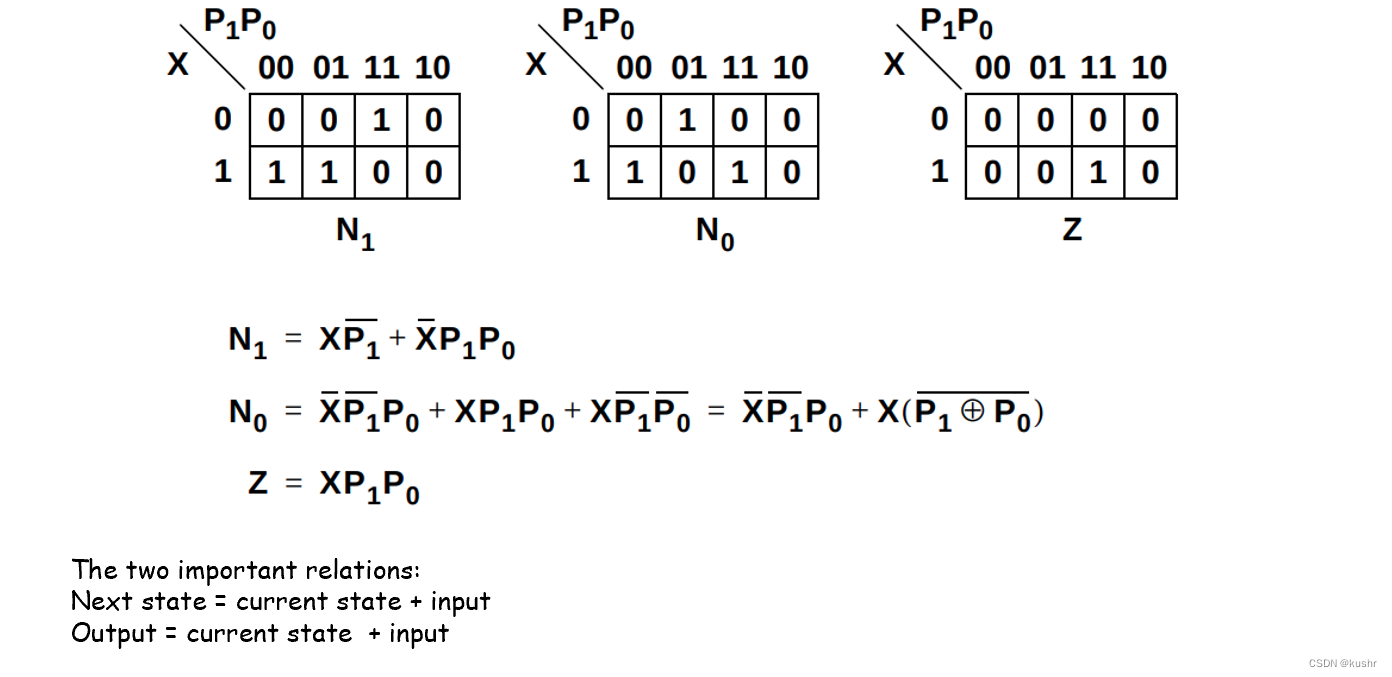
Seq circuit design
一些qnext与输入的关系:
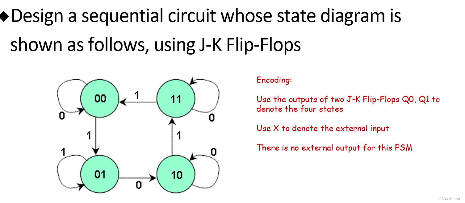
Design a sequential circuit
顺序:
1、写FSM的table(present state,next state,input)
2、列出ff的excitation table(q,qnext,input)
3、根据FSM table的present state和next state的关系,对照ff table,找出每个ff的输入
4、由大table中得出每个ff输入的switch func
5、画出电路图
Example:
步骤1,2:
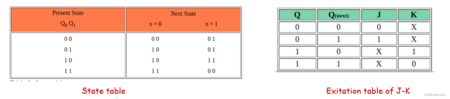
步骤3:
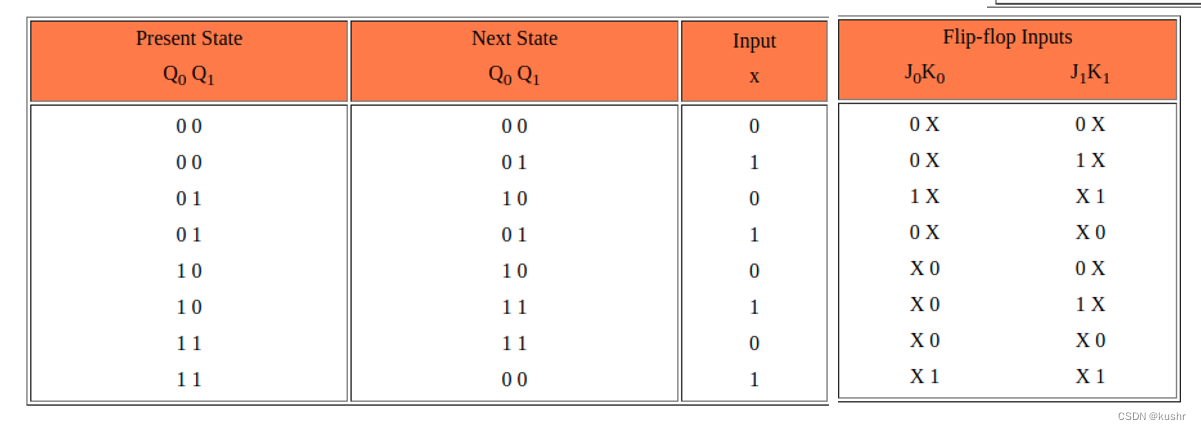
解释:这里有两个jk的ff,ff0和ff1,因此对应四个输入,j0,k0, j1,k1, 从上表中可以看出:
第一行中,q0从0变到0,因此根据ff table,j0k0分别是0,x 。
q1从0变到0,因此根据ff table,j1k1分别是0,x 。
第二行中,q0从0变到0,因此根据ff table,j0k0分别是0,x 。
q1从0变到1,因此根据ff table,j1k1分别是1,x 。
第三行中,q0从0变到1,因此根据ff table,j0k0分别是1,x 。
q1从1变到0,因此根据ff table,j1k1分别是x,1 。
…以此类推
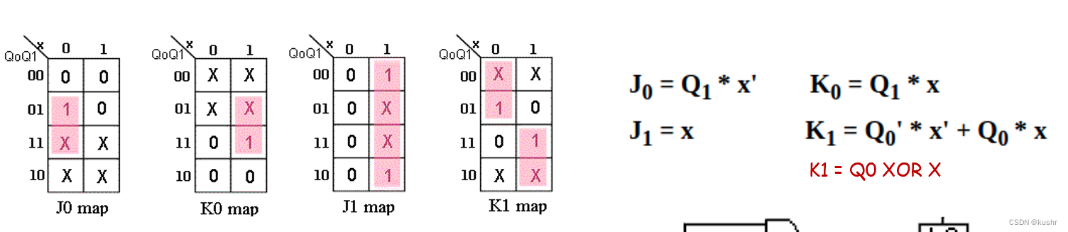
步骤4:画kmap(q0q1用present),算fuction
步骤5:画电路
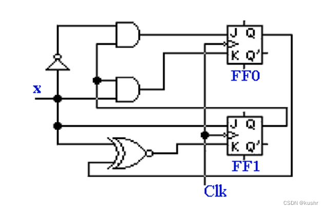
hint:这一步可以在logism里用boolean func 完成
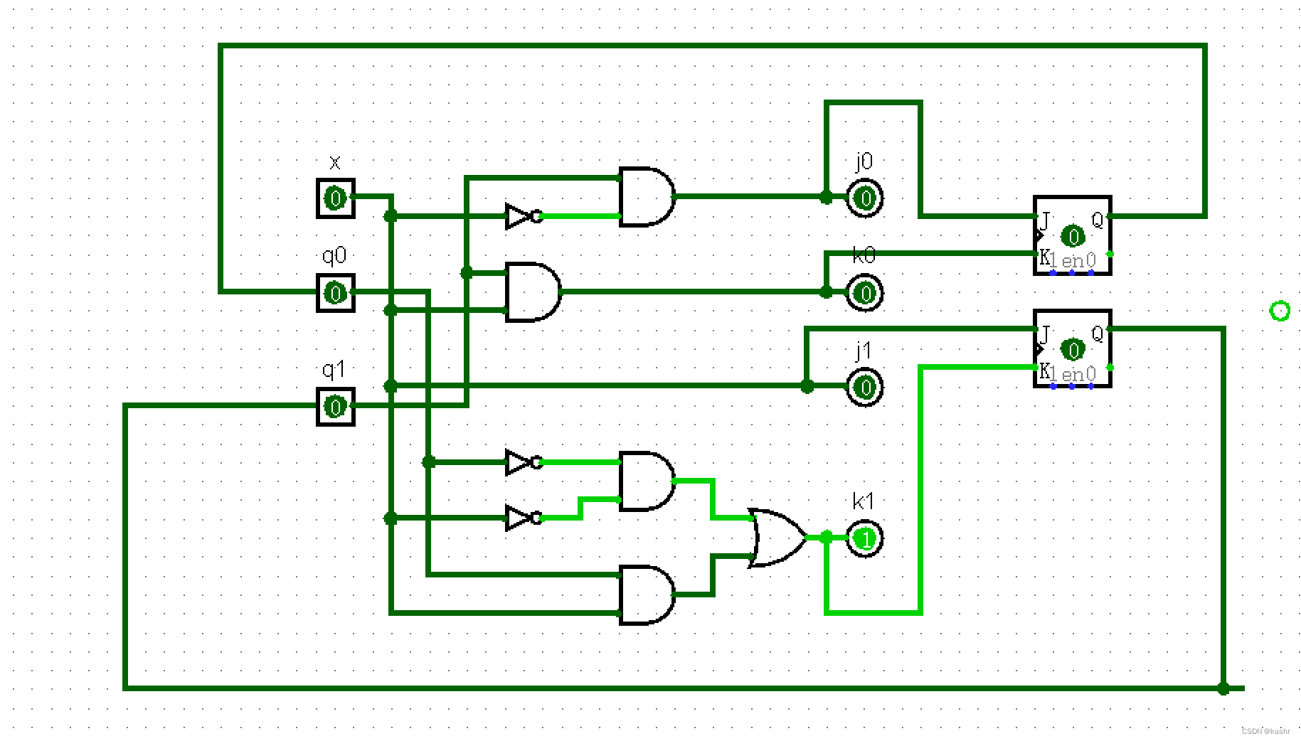
project-analyze circuit -table
ff在memory里(q0和q1输入一个没有小方块,这样只是方便看)
lec9 Computer Memory (I):Memory hierarchy and Cache
- Memory can be categorized based on Technologies
- SRAM (Static Random Access Memory)
- DRAM (Dynamic Random Access Memory)
- PROM (Programmable Read-Only Memory)
- Magnetic Disk
Memory can be categorized based on Technologies
SRAM (Static Random Access Memory)
DRAM (Dynamic Random Access Memory)
PROM (Programmable Read-Only Memory)
Magnetic Disk
Measures of Performance – Access Time (latency)
random access:一个指令(读/写)的时间
non random access:从发出指令到到达指令地点的时间
memory cycle time:指令1发起到指令二可以发起的时间
transfer rate:1/memory cycle time
**Physical features – **
volatile:非永久(寄存器,ram’)
non volatile:永久(硬件)
erasable:可以被重写或删除:register/硬盘(hard drive)
non erasable:不能被重写(ROM:read only),CD
internal: registers in processor, main memory, cache
external: the peripheral storage devices, such as disk and tape – they are accessible to the processor via I/O controllers
memory hierarchy
1:expose hierarchy
programmer决定如何分配
2、hide hierarchy

cache memory
在靠近cpu的地方
先找cache-找不到去memory(按block找),将word放入cache

最小单位:word
每个word有n bit的地址,所以memory是2^n的形式
block:含有k个word;M=2^n/k blocks
cache有m行,每行都有k个word(block含有的数量)
cach中有m行,memory中有M个block,m<<M。
mapping
direct mapping
注意,cache的一个line里只能储存一个block
内存的block被分配到规定的cache line
例如,q=m/M,q个block被分配到一个cache line里
Equivalently, the mapping can be implemented through modular operation:


w:word number within block (2^w words)快中第几个字
s:s bits = block number (2^s blocks)内存第几块
r:identify the line number in Cache(2^r line in chache)缓存第几行
s-r:Tag for a line in Cache: which block this line is currently storing
s-r = cache line number, s = main memory block number, r = number of lines in cache
s(对应的数) mod(2^r)=r

最小单位:byte
associate mapping
不固定
address = s + w bits; 2^s blocks in memory
measurement of cache
miss rate: l1<0.01, l2 0.03-0.05…
Replacement Algorithms for Associative Mapping
Least Recently Used (LRU)
First-in-first-out (FIFO)
Least Frequently Used (LFU)
lec10:Internal and External Memory
internal
memory cells:


ram
dynamic ram cell(DRAM):需要refresh

static RAM cells
不需要refresh

DRAM vs. SRAM
Common: volatile – need continuous power
Difference:
DRAM cell is simpler and smaller, thus denser (more cells per unit area) and less expensive
however, DRAM requires the supporting refresh circuitry
DRAM tends to be favored for large memory requirement
DRAM for main memory, SRAM for cache
rom:Read-Only Memory
不可改变不可删除
Usage
system programs
library subroutines for frequently wanted functions
Programmable ROM (PROM)
Read-Mostly Memory (a variation of ROM):EPROM、EEPROM、flash memory
Erasable Programmable ROM (EPROM)


chip logic


 1101
1101


 被折叠的 条评论
为什么被折叠?
被折叠的 条评论
为什么被折叠?
 到【灌水乐园】发言


