


EJTAG
:
MIPS extension
of JTAG.
It exploits the infrastructure provided by the IEEE 1149.1 JTAG Test Access Port (TAP) standard to provide an external interface, and extends the MIPS instruction set and privileged resource architectures to provide a standard software architecture for integrated system debugging.
《
see mips run
》
在阅读本文之前请先阅读:
jtag
接口标准
.docx
“EJTAG”
之前的调试支持
---
断点指令和
CP0
观察点
Mips
体系架构在
EJTAG
调试单元出现之前就已经存在了许多年,所以还有一些传统的调试功能,这包括
break
指令,这个指令只是简单导致一个异常,
cpu
同时也实现了多达四个的硬件观察点,由几个
CP0
寄存器控制,每个观察点指定一个虚拟地址,可以用于在每次取指,存储和加载操作中检查,如果地址匹配就会触发异常,与
EJTAG
观察点相比,不能进行模糊地址匹配,当然了观察点触发后只是引起普通异常,所以不能用于调试异常处理。
EJTAG Components and Options
EJTAG hardware support consists of several distinct components: extensions to the MIPS processor core, the EJTAG Test Access Port, the Debug Control Register, and the Hardware Breakpoint Unit.
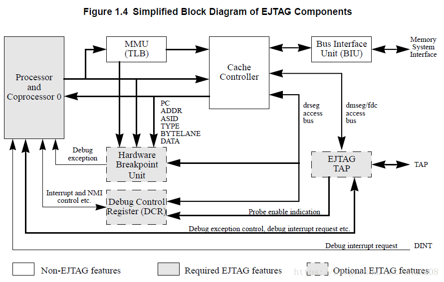
- EJTAG Processor Core Extensions
A MIPS processor or core supporting EJTAG
must support :
• Debug Mode, associated exceptions and dedicated debug vector
• Instruction set extensions: SDBBP (Software Debug Breakpoint) and DERET (Debug Exception Return)
• CP0 registers: Debug, DEPC and DESAVE
The following implementation-dependent
options
:
• Memory-mapped debug segment (dseg) (optional)
• The single-step execution feature is optional. The presence or absence of single step execution capability is indicated to debug software via the CP0 Debug register.
• The debug interrupt request from the TAP via the DINT probe signal or through an implementation-dependent internal signal is optional.
•
The Test Access Port (TAP) is optional
.
• The Hardware Breakpoint Unit (HBU) is optional. Note that it is required if the CBT is implemented.
• The Complex Break and Trigger (CBT) block is optional.
•
The Debug Control Register (DCR) is optional
. Note that it is required if either the HBU or the CBT is implemented.
• The PC Sampling feature of EJTAG is optional.
• The Fast Debug Channel feature of EJTAG is optional.
-
Debug Exception and Debug Mode
Debug Mode is entered only through a debug exception. It is exited as a result of either the execution of a DERET instruction or application of a reset or soft reset.
When the processor is operating in Debug Mode, it has access to the same resources, instructions, and CP0 registers as it has in Kernel Mode. The restrictions on Kernel Mode accesses (non-zero coprocessor references, access to extended addressing controlled by UX, SX, KX, etc.) apply equally to Debug Mode, but Debug Mode provides some additional capabilities described in this chapter.
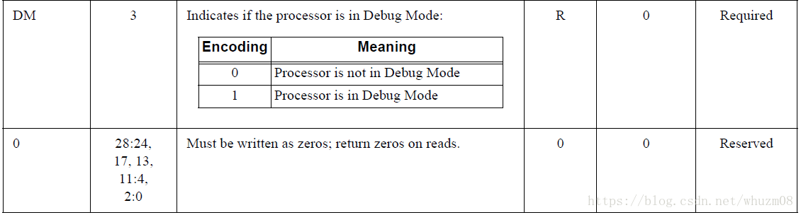
Other processor modes (Kernel Mode, Supervisor Mode, User Mode) are collectively considered as Non-Debug Mode. Debug software can determine if the processor is in Non-Debug Mode or Debug Mode through the DM bit in the Debug register
触发
debug
异常的条件有:执行指令(
break
,
SDBBP
),硬件断点,外部
DINT
中断
debug
异常处理流程
Debug Mode Address Space
Debug Mode access to unmapped address space is identical to that of Kernel Mode. Mapped addresses are accessible as in Kernel Mode.
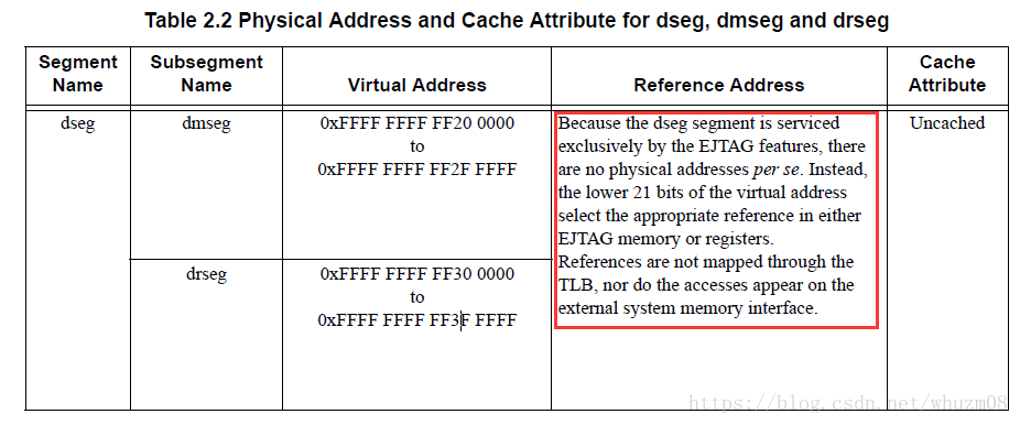
In addition, an optional uncached and unmapped debug segment dseg (EJTAG area) appears in the address range 0xFFFF FFFF FF20 0000 to 0xFFFF FFFF FF3F FFFF. The dseg segment thereby appears in the kseg part of the compatibility segment
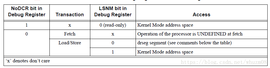
The implementation-dependent value of the NoDCR bit in the Debug register indicates the presence of the dseg segment , If the dseg segment is not present, then all transactions from the processor in Debug Mode go to the Kernel Mode address space. Debug software must check the DebugNoDCR bit before trying to access the dseg segment.
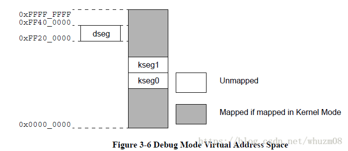
The dseg segment is subdivided into dmseg (EJTAG memory) segment and the drseg (EJTAG registers) segment. The dmseg segment is used when the probe services the memory segment. The drseg segment is used when the memory-mapped debug registers are accessed.
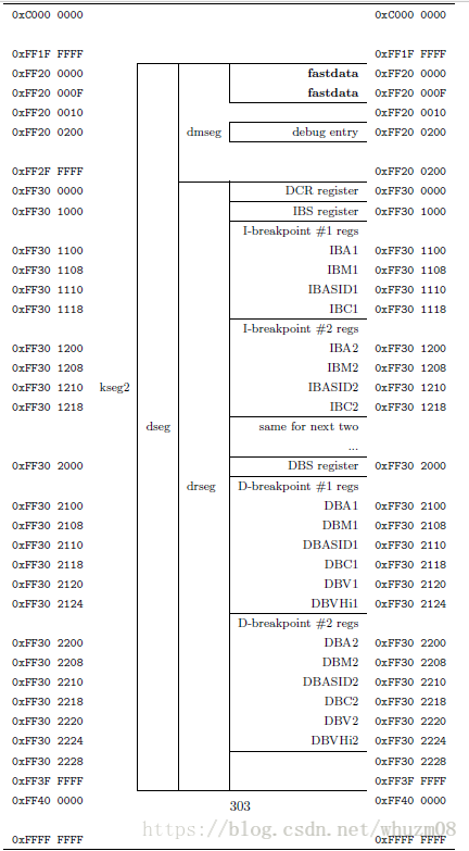
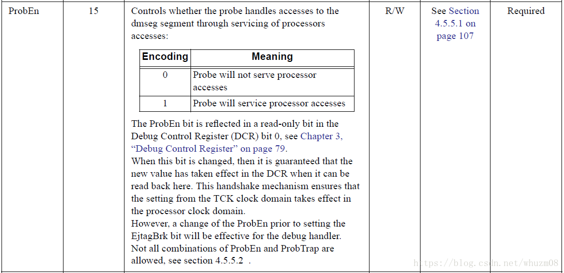
Access to dmseg (EJTAG memory) Address Range
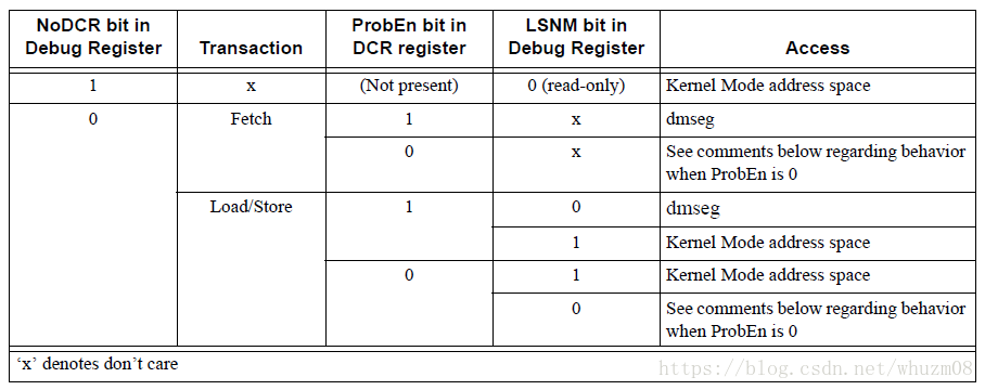
when ProbEn equals 0 for dmseg segment accesses, debug software accessed the dmseg segment
when the ProbEn bit was 0, indicating that there is no probe available to service the request. Debug software must read the state of the ProbEn bit in the DCR register before attempting to reference the dmseg segment. However, accessing the dmseg segment while ProbEn is 0 can occur because there is an inherent race between the debug software sampling the ProbEn bit as 1 and the probe clearing it to 0. The probe can therefore not assume that a reference to the dmseg segment never occurs if the ProbEn bit is dynamically cleared to 0. If debug software references the dmseg segment when ProbEn is 0, the reference hangs until it is satisfied by the probe.
Access to drseg (EJTAG Registers) Address Range
Instruction fetches from drseg are not allowed. The operation of the processor is UNDEFINED if the processor attempts am instruction fetch from the drseg segment.
When the NoDCR bit is 0 in the Debug register, it indicates that the processor is allowed to access the entire drseg segment, and therefore a response occurs to all transactions in the drseg segment.
The DCR register, at offset 0x0000 in the drseg segment, is always available if the dseg segment is present. Debug software is expected to read the DCR register to determine what other memory-mapped registers exist in drseg.
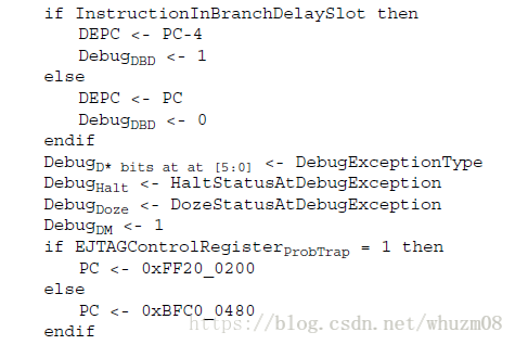
Exceptions Taken in Debug Mode
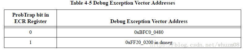
The handling of exceptions generated in Debug Mode, other than through resets and soft resets, differs from those exceptions generated in Non-Debug Mode in that only the Debug and DEPC registers are updated. All other CP0 registers are unchanged by an exception taken in Debug Mode. The exception vector is equal to the debug exception vector (see
Section 2.3.2 on page 44
), and the processor stays in Debug Mode.
Only some Non-Debug Mode exception events cause exceptions in Debug Mode. Remaining events are blocked.
It is the responsibility of the debug handler to save the contents of the Debug, DEPC, and DESAVE registers before nested entries into the handler at the debug exception vector can occur. The handler returns to the debug exception handler by a jump instruction, not a DERET, in order to keep the processor in Debug Mode.
Exceptions on Imprecise Errors
Exceptions on imprecise errors are possible in Debug Mode due to a bus error on an instruction fetch or data access, cache error, or machine check.
The IEXI bit in the Debug register blocks imprecise error exceptions on entry or re-entry into Debug Mode. They can be re-enabled by the debug exception handler after sufficient context has been saved to allow a safe re-entry into Debug Mode and the debug handler.
Pending exceptions due to instruction fetch bus errors, data access bus errors, cache errors, and machine checks are indicated and controlled by the IBusEP, DBusEP, CacheEP and MCheckP bit in the Debug register
-
Debug Breakpoint Instruction
EJTAG introduces a new breakpoint instruction, SDBBP, which differs from the MIPS32 and MIPS64 BREAK instruction in that the resulting exception, like the single-step and hardware breakpoint debug exceptions described below, places the processor in Debug Mode and can fetch its associated handler code from EJTAG memory.
-
EJTAG Coprocessor 0 Registers
Debug----
有配置和控制位
DEPC-----debug exception
结束后返回的地址,供
deret
指令使用
DSAVE----
供
debug
异常服务处理函数作为临时寄存器保存其他通用寄存器的内存,这样其他通用寄存器就可以使用了
下面重点讲一下
Debug
这个寄存器:
The Debug register is used to control the debug exception and provide information about the cause of the debug
exception.
Only the DM bit and the EJTAGver field are valid when read from non-debug mode; the value of all other bits and fields is UNPREDICTABLE. Operation of the processor is UNDEFINED if the Debug register is written from non-debug
mode.
Some of the bits and fields are only updated on debug exceptions and/or exceptions in debug mode, as shown below:
• DSS, DBp, DDBL, DDBS, DIB, DINT are updated on both debug exceptions and on exceptions in debug modes
• DExcCode is updated on exceptions in debug mode, and is undefined after a debug exception
• Halt and Doze are updated on a debug exception, and is undefined after an exception in debug mode
• DBD is updated on both debug and on exceptions in debug modes
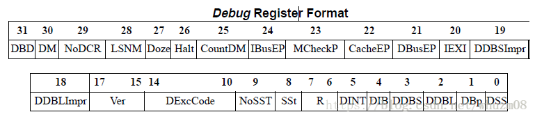
NoDCR:
为只读
bit
,指示
dseg
是否存在
LSMN
:如果你想要
dseg
消失,设置该
bit
为
1
,即使在
debug
模式也行,以便能访问被覆盖的内存区,这会使得
EJTAG
的控制系统大部分不能使用,所以只能在某个特定的
load/store
指令前后使用
IEXI
:该
bit
置
1
时推迟非精确异常。缺省情况下进入调试模式时置
1
,离开时清
0
,但是可写,一旦该位清零,被推迟的异常立刻发生,在置
1
时,推迟的异常可以通过异常
pend bit
查看到:

DSS, DBp, DDBL, DDBS, DIB, DINT
:
引起
debug
异常的原因,只读
bit
,记录是什么原因引起了
debug
异常
DExcCode
:记录在
debug
异常中发生其他非
debug
异常的原因,正常情况下是记录在
cause
寄存器的
ExcCode
字段中,第一次进入
debug
异常时,该字段的值未定义
- EJTAG Test Access Port
EJTAG
说白了就是在
JTAG
的基础上增加了指令和对应的寄存器,以增加额外的调试功能,因此
TAP
和
TAP controler
是相同的:
下面挑几个来讲
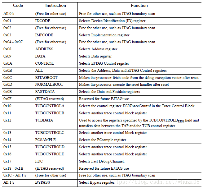
Data Register (TAP Instruction DATA, ALL, or FASTDATA)
The read/write Data register is used for opcode and data transfers during processor accesses. The width of the Data register is 32 bits for 32-bit processors and 64 bits for 64-bit processor.
The value read in the Data register is valid only if a processor access for a write is pending, in which case the data register holds the store value. The value written to the Data register is only used if a processor access for a pending read is finished afterwards, in which case the data value written is the value for the fetch or load. This behavior implies that the Data register is not a memory location where a previously written value can be read afterwards.
Address Register (TAP Instruction ADDRESS or ALL)
The read-only Address register provides the address for a processor access. The width of the register corresponds to the size of the physical address in the processor implementation (from 32 to 64 bits). The specific length is determined by shifting through the Address register, because the length is not indicated elsewhere.
The value read in the register is valid if a processor access is pending; otherwise, the value is undefined.
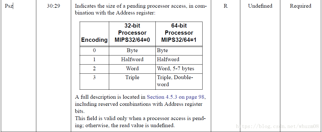
The two or three LSBs of the register are used with the Psz field from the EJTAG Control register to indicate the size and data position of the pending processor access transfer. These bits are not taken directly from the address referenced by the load/store.
EJTAG Control Register (ECR) (TAP Instruction CONTROL or ALL)
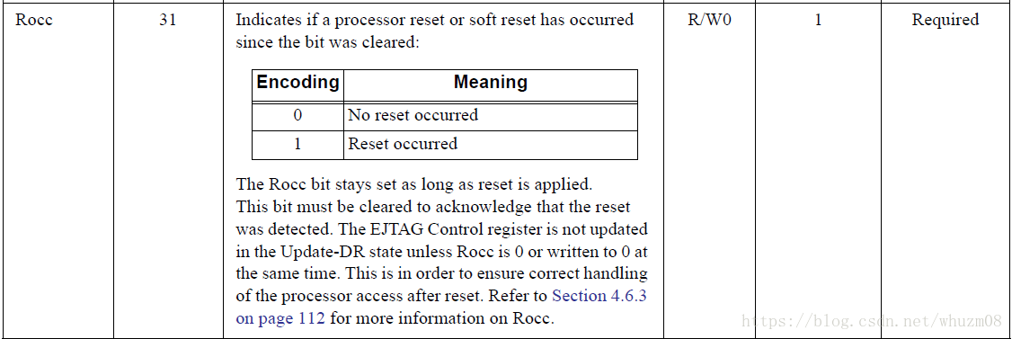
The 32-bit EJTAG Control Register (ECR) handles processor reset and soft reset indication, Debug Mode indication, access start, finish, and size and read/write indication. The ECR also:
• controls debug vector location and indication of serviced processor accesses,
• allows a debug interrupt request,
• indicates processor low-power mode, and
• allows implementation-dependent processor and peripheral resets.
The EJTAG Control register is not updated/written in the Update-DR state unless the Reset occurred; that is Rocc (bit 31) is either already 0 or is written to 0 at the same time. This condition ensures proper handling of processor accesses after a reset.


- Debug Control Register
The Debug Control Register (DCR) is a memory-mapped register that can be implemented as part of either the processor core or an external logic block. It indicates the availability and status of EJTAG features. The memory-mapped region containing the DCR is available to software only in Debug Mode.
The presence or absence of the DCR is indicated in the CP0 Debug register.
- Hardware Breakpoint Unit
The Hardware Breakpoint Unit implements memory-mapped registers that control the instruction and data hardware breakpoints. The memory-mapped region containing the hardware breakpoint registers is accessible to software only in Debug Mode.
The presence or absence of hardware breakpoint capability is indicated to debug software in the DCR.
- Hardware Breakpoints
Hardware breaks on instructions have the advantage over software debug breaks in that it is possible to set them in any address area. Furthermore, if memory cannot be altered by inserting SDBBP codes, the hardware breaks can still be used. Hardware data breakpoints allow breaks on load/store operations.
EJTAG implements two kinds of simple breaks:
• Instruction breaks, in which a break may be set on an instruction fetch from a specific virtual address
• Data breaks, in which a break may be set on a load/store reference from a specific virtual address, which additionally can be qualified by a data value.
There may be up to 15 break channels of each type implemented, and each break channel may be programmed with address, address mask, ASID, and reference type.
EJTAG specification 4.00 and above also define complex breakpoints. There are many different types of complex breakpoints defined the complex break chapter. Like the simple breaks, the complex breaks can cause a trigger signal that can be used to enable or disable tracing via the MIPS PDtrace architecture.
-
Fast Debug Channel
EJTAG version 5.0 adds the optional Fast Debug Channel (FDC) mechanism for data transfer between a debug host/probe and a target. The FDC mechanism allows the user to set up a data transfer, and then resume normal operation. The data transfer occurs in the background, and the target CPU can either choose to check the status of the transfer periodically, or it can choose to be interrupted at the end of the transfer.
The FDC mechanism adds two First In First Out (FIFO) structures that are mapped into the target CPU physical address map. The probe uses the new FDC TAP instruction to access these FIFOs, while the CPU itself accesses them using memory accesses.
When compared with the pre-existing FASTDATA mechanism (See
Section 4.4.3 “FASTDATA Instruction”
), the primary advantage of FDC is that it does not require the CPU to be blocked when the probe is reading or writing to the data transfer FIFOs. This significantly reduces the CPU overhead and makes data transfers far less intrusive to the code executing on the CPU.
- Complex Breakpoint and Trigger (CBT) Block
The presence or absence of this optional block is indicated by a bit (10) in the DCR register. Each of the listed features of this block is optional and the presence or absence of this feature is indicated by bits in the CBTcontrol register which is a drseg address-mapped register at address 0x8000.
- Pc sample
PC
取样提供了一种不影响程序正常执行的方式来搜集正在运行的系统活动的统计信息,
PC
取样周期性的查看当前
pc
的值,把这个值记录到探针可以检索到的地方,然后由软件构造一段时间内的取样直方图,能够在统一意义上让程序员看到
cpu
在什么地方花费了最多的时钟周期。这个功能不仅有用,而且大家非常熟悉:以前好多年系统都是基于中断的
PC
取样,这种方式对程序运行有影响。取样频率由
DCR
寄存器中的一些域来控制。
- PDtrace
PDtrace
可以跟踪程序的执行,
pc sample
只能记录执行
pc
,但是
PDtrace
也能跟踪读写地址甚至读写的数据值。
跟踪执行并不需要很多数据,假定分析程序拥有被跟踪程序的二进制代码,所以当顺序执行时只需要知道
cpu
顺序走了多远,当遇到条件分支时,只需要知道条件是否满足,但是对于寄存器跳转之类的指令,跟踪需要记录完整的地址。
跟踪信息记录到片上的存储器虽然简单快速,但是由于片上缓存器都很小,通常只能记录程序运行的很小一段时间。当把跟踪信息送到探针可以取的地方时,就可以一直记录。
- Single-Step Execution
EJTAG provides support for single-step execution of programs and operating systems, without requiring that the code reside in RAM.
- EJTAG怎么控制cpu
1.
探针会用
JTAG
设置
ECR
寄存器标志(
ProbTrap
),让调试异常入口为
0XFF20 0200-----
位于
dmseg
,然后探针可以设置
ECR
(
EjtagBrk
)请求进入调试异常,或者设置一个调试断点或硬件观察点触发进入调试异常,这时调试异常从
dmseg
取指令开始执行,这样探针就获得了控制权。
2.
探针可以发送一个
EJTAGBOOT
命令,然后等待下一次
CPU
复位之后,
CPU
就从
dmseg
读取指令。
- 怎么从probe(dmseg)中执行代码
1. pc
机端,通过读
ejtag
的
ECR
控制寄存器
(ir=10)
,注意读的同时会串入一个新值,看读回来的
DM(bit3)
是否为
1,
为1则表明系统已经处在
debug
模式中
,goto 3,
否则
goto 2
2.
写
ECR(ir=10),
设置
ProbTrap (bit14)1,
使得
debug
异常向量指向
FF20 0200
(位于
dmseg
),然后设置
EjtagBrk
为
(bit12)
1,向系统请求
debug
异常,
goto 1
3.
查看
ECR
寄存器的
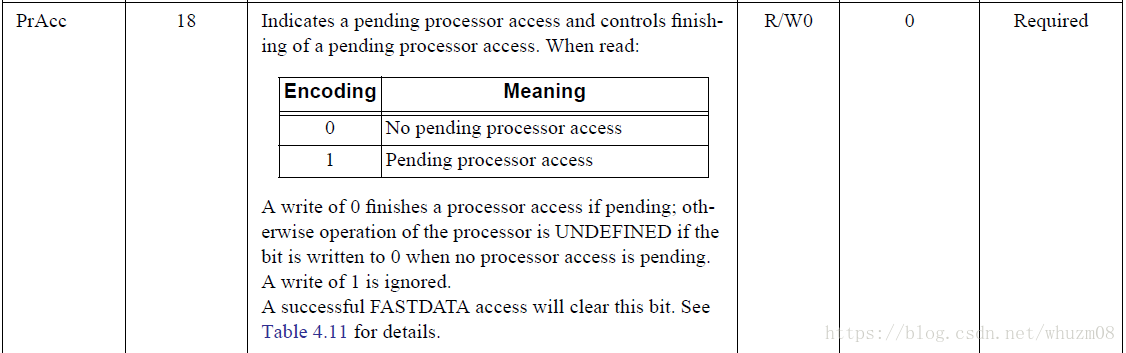
PrAcc (bit 18)
是否为1,为
1
则表明
cpu
向
ejtag dmseg
地址发出访问
,ECR
寄存器的
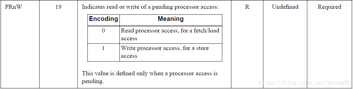
PRnW (bit19)
表明是读还是写,
Psz (bit 30:29)
表明访问宽度
, goto 4,
否则
goto 1
4.
读
ejtag
的
address reg(ir=8)
到
addr
变量,得到
cpu
想要访问的地址
,
如果是写操作
goto 5,
否则读操作
goto 6
5.
读
ejtag
的
data reg(ir=9),
读出写过来的内容
,
如果地址大于
0xff200200,(addr-0xff200200)/4
是
codebuf
偏移
offs,
则
codebuf[offs]=data,
如果地址小于
0xff200200,param,stack=data
等
,goto 7
6.
如果地址大于
0xff200200,(addr-0xff200200)/4
是
codebuf
偏移
offs,
则
data=codebuf[offs],
如果地址小于
0xff200200,data=param,stack
等
,
将
data
写入
ejtag data reg(ir=10),goto 7
7.
写
ECR
寄存器,清掉
PrAcc
位,这样
cpu
这次访存操作就完成了。


 242
242

 被折叠的 条评论
为什么被折叠?
被折叠的 条评论
为什么被折叠?
 到【灌水乐园】发言


