


1、模块概述
SPI接口模块用于连接flash芯片(从机)与FPGA(主机),实现主从机之间的串口通信。
考虑到分别于主机和从机连接所以端口可分为两部:
(1)与flash_control模块连接端口(主机部分)
| input/output | name | description |
| input | req | 读写请求信号 |
| input | din[7:0] | 输入的命令、地址、写入数据等 |
| output | done | 一字节(8bit)传输完成标志 |
| output | dout[7:0] | 接收m25p16反馈数据后发送回主机(串转并) |
(2)与m25p16连接端口(从机部分)
| input/output | name | description |
| input | miso | m25p16反馈的串行数据 |
| output | cs_n | 片选信号(低有效),拉低时才能进行读写等操作 |
| output | mosi | 输入的命令、地址、写入数据等(并转串) |
| output | sclk | 主机产生时钟信号(16分频) |
2. 主要完成任务
(1)产生时钟分频驱动主从设备
由上片文章可知,需要20MHz及以下时钟频率才能同时满足读写操作,且m25p16支持SPI工作模式0和3。
本设计采用16分频和SPI工作模式3,使用计数器实现分频代码如下:
//****************************************************************
//--cnt_freq
//****************************************************************
    always @(posedge clk or negedge rst_n)begin
       if(!rst_n)begin
            cnt_freq <= 5'd0;
        end
        else if(add_cnt_freq)begin
            if(end_cnt_freq)begin
                cnt_freq <= 5'd0;
            end
            else begin
                cnt_freq <= cnt_freq + 1'b1;
            end
        end
    end

    assign add_cnt_freq = req;
    assign end_cnt_freq = add_cnt_freq && cnt_freq == `FREQUENCY;

//****************************************************************
//--sclk_reg 采用SPI通信模式3  下降沿发送,上升沿采样
//****************************************************************
    always @(posedge clk or negedge rst_n)begin
        if(!rst_n)begin
            sclk_reg <= 1'b1;                 //初始高电平
        end
        else if(cnt_freq == `SCLK_FALL)begin
            sclk_reg <= 1'b0;                 //flash m25p16 下降沿 数据改变
        end
        else if(cnt_freq == `SCLK_RISE)begin
            sclk_reg <= 1'b1;                 //flash m25p16 上升沿 数据稳定
        end
    end
(二)并串互转
a. 将主机发送的并行数据(指令、地址、写入数据等),转换成串行数据发送给m25p16;
b. 将m25p16反馈的串行数据(ID、状态寄存器、读出数据等),转换成并行数据发送给主机
使用bit计数器实现代码如下:
//****************************************************************
//--cnt_bit
//****************************************************************
    always @(posedge clk or negedge rst_n)begin
       if(!rst_n)begin
            cnt_bit <= 'd0;
        end
        else if(add_cnt_bit)begin
            if(end_cnt_bit)begin
                cnt_bit <= 'd0;
            end
            else begin
                cnt_bit <= cnt_bit + 1'b1;
            end
        end
    end

    assign add_cnt_bit = end_cnt_freq;
    assign end_cnt_bit = add_cnt_bit && cnt_bit == `MUX_BIT;

//****************************************************************
//--tx_data
//****************************************************************
    always @(posedge clk or negedge rst_n)begin
        if(!rst_n)begin
            tx_data <= 8'b0;
        end
        else if(req && cnt_freq == `SCLK_FALL)begin
            tx_data <= din;
        end
    end

    assign  mosi = tx_data[4'd7-cnt_bit];

//****************************************************************
//--rx_data
//****************************************************************
    always @(posedge clk or negedge rst_n)begin
        if(!rst_n)begin
            rx_data <= 8'b0;
        end
        else if(req && cnt_freq == `SCLK_RISE)begin
            rx_data[4'd7-cnt_bit] <= miso;
        end
    end
(三)片选信号(cs_n)及一字节传输完成信号(done)
使用比特计数器计数传输的bit数,当传输完8bit后done信号拉高一周期,当读写请求信号有效状态下,cs_n拉低,代码实现如下:
//****************************************************************
//--cnt_bit
//****************************************************************
    always @(posedge clk or negedge rst_n)begin
       if(!rst_n)begin
            cnt_bit <= 'd0;
        end
        else if(add_cnt_bit)begin
            if(end_cnt_bit)begin
                cnt_bit <= 'd0;
            end
            else begin
                cnt_bit <= cnt_bit + 1'b1;
            end
        end
    end

    assign add_cnt_bit = end_cnt_freq;
    assign end_cnt_bit = add_cnt_bit && cnt_bit == `MUX_BIT;

    assign  cs_n = ~req       ;
    assign  done = end_cnt_bit;
3. 模块代码
/**************************************功能介绍***********************************
Description: SPI协议接口模块
Change history: 2023年7月13日
*********************************************************************************/

`include "param.v"

//---------<模块及端口声名>------------------------------------------------------
module spi_interface(
    input				clk		    ,
    input				rst_n	    ,
    //flash_control接口
    input               req         ,//操作请求信号
    input      [7:0]    din         ,//输入数据(命令 地址  ID 写数据)
    output              done        ,//传输完成一个字节数据标志信号
    output     [7:0]    dout        ,//接受到的flash数据串转并
    //flash芯片 接口
    input				miso	    ,//从机(flash)信号
    output		     	cs_n	    ,//主机发送片选信号
    output		     	mosi	    ,//主机发送数据  并转串
    output		    	sclk	     //主机产生时钟信号
);
//---------<内部信号定义>-----------------------------------------------------
    //分频计数器
    reg			[4:0]	cnt_freq	;
    wire				add_cnt_freq;
    wire				end_cnt_freq;
    //spi输出信号寄存
    reg                 sclk_reg    ;//串行同步时钟
    //寄存flash发送过来的数据
    reg         [7:0]   rx_data     ;//寄存dout
    //寄存控制模块发送过来的数据
    reg         [7:0]   tx_data     ;
    //字节计数器
    reg			[3:0]	cnt_bit	   	;
    wire				add_cnt_bit	;
    wire				end_cnt_bit	;

//****************************************************************
//--cnt_freq
//****************************************************************
    always @(posedge clk or negedge rst_n)begin
       if(!rst_n)begin
            cnt_freq <= 5'd0;
        end
        else if(add_cnt_freq)begin
            if(end_cnt_freq)begin
                cnt_freq <= 5'd0;
            end
            else begin
                cnt_freq <= cnt_freq + 1'b1;
            end
        end
    end

    assign add_cnt_freq = req;
    assign end_cnt_freq = add_cnt_freq && cnt_freq == `FREQUENCY;

//****************************************************************
//--cnt_bit
//****************************************************************
    always @(posedge clk or negedge rst_n)begin
       if(!rst_n)begin
            cnt_bit <= 'd0;
        end
        else if(add_cnt_bit)begin
            if(end_cnt_bit)begin
                cnt_bit <= 'd0;
            end
            else begin
                cnt_bit <= cnt_bit + 1'b1;
            end
        end
    end

    assign add_cnt_bit = end_cnt_freq;
    assign end_cnt_bit = add_cnt_bit && cnt_bit == `MUX_BIT;

//****************************************************************
//--sclk_reg 采用SPI通信模式3  下降沿发送,上升沿采样
//****************************************************************
    always @(posedge clk or negedge rst_n)begin
        if(!rst_n)begin
            sclk_reg <= 1'b1;                 //初始高电平
        end
        else if(cnt_freq == `SCLK_FALL)begin
            sclk_reg <= 1'b0;                 //flash m25p16 下降沿 数据改变
        end
        else if(cnt_freq == `SCLK_RISE)begin
            sclk_reg <= 1'b1;                 //flash m25p16 上升沿 数据稳定
        end
    end

//****************************************************************
//--tx_data
//****************************************************************
    always @(posedge clk or negedge rst_n)begin
        if(!rst_n)begin
            tx_data <= 8'b0;
        end
        else if(req && cnt_freq == `SCLK_FALL)begin
            tx_data <= din;
        end
    end

//****************************************************************
//--rx_data
//****************************************************************
    always @(posedge clk or negedge rst_n)begin
        if(!rst_n)begin
            rx_data <= 8'b0;
        end
        else if(req && cnt_freq == `SCLK_RISE)begin
            rx_data[4'd7-cnt_bit] <= miso;
        end
    end

//****************************************************************
//--sclk  cs_n  mosi  done  dout
//****************************************************************
    assign  sclk = sclk_reg   ;
    assign  cs_n = ~req       ;
    assign  mosi = tx_data[4'd7-cnt_bit];
    assign  done = end_cnt_bit;
    assign  dout = rx_data    ;


endmodule
4. 模块仿真
调用m25p16从机模型进行命令发送机数据接收仿真。
仿真代码如下:
`timescale 1ns/1ns

module tb_spi_interface();

    reg				tb_clk	;
    reg				tb_rst_n;
    //flash_control接口
    reg             req     ;
    reg      [7:0]  din     ;
    wire            done    ;
    wire     [7:0]  dout    ;
    //flash芯片 接口
    wire			miso	;
    wire		    cs_n	;
    wire		    mosi	;
    wire		    sclk	;

    pullup(miso);
    //pulldown(miso);

//时钟周期参数定义
    parameter		CLOCK_CYCLE = 20;

//模块例化
    spi_interface spi_interface_inst(
    .clk  	(tb_clk  ) ,
    .rst_n	(tb_rst_n) ,
    .req    (req     ) ,//操作请求信号
    .miso   (miso    ) ,
    .din    (din     ) ,//输入数据(命令 地址  ID 写数据)
    .done   (done    ) ,//传输完成一个字节数据标志信号
    .dout   (dout    ) ,//接受到的flash数据串转并
    .cs_n	(cs_n	 ) ,//主机发送片选信号
    .mosi	(mosi	 ) ,//主机发送数据  并转串
    .sclk	(sclk	 )  //主机产生时钟信号
);

    m25p16 m25p16_inst(
   /*input */.c       (sclk    ),
   /*input */.data_in (mosi    ),
   /*input */.s       (cs_n    ),
   /*input */.w       (        ),
   /*input */.hold    (        ),
   /*output*/.data_out(miso    )
    );

//产生时钟
    initial 		tb_clk = 1'b0;
    always #(CLOCK_CYCLE/2) tb_clk = ~tb_clk;

//产生激励
    initial  begin
        tb_rst_n = 1'b1;
        req  = 1'b0;
        din  = 8'b0;
        #(CLOCK_CYCLE*2);
        tb_rst_n = 1'b0;
        #(CLOCK_CYCLE*20);
        tb_rst_n = 1'b1;
        #3;

        //模拟输入指令
        req = 1'b1 ;
        din = 8'h03;//输入读数据命令
        @(negedge done);
        din = 8'h00;//高位地址
         @(negedge done);
        din = 8'h00;//中位地址
         @(negedge done);
        din = 8'h01;//低位地址
        #(CLOCK_CYCLE*1000);
        req = 1'b0;
        #(CLOCK_CYCLE*100);
        $stop;


    end

endmodule
仿真结果:
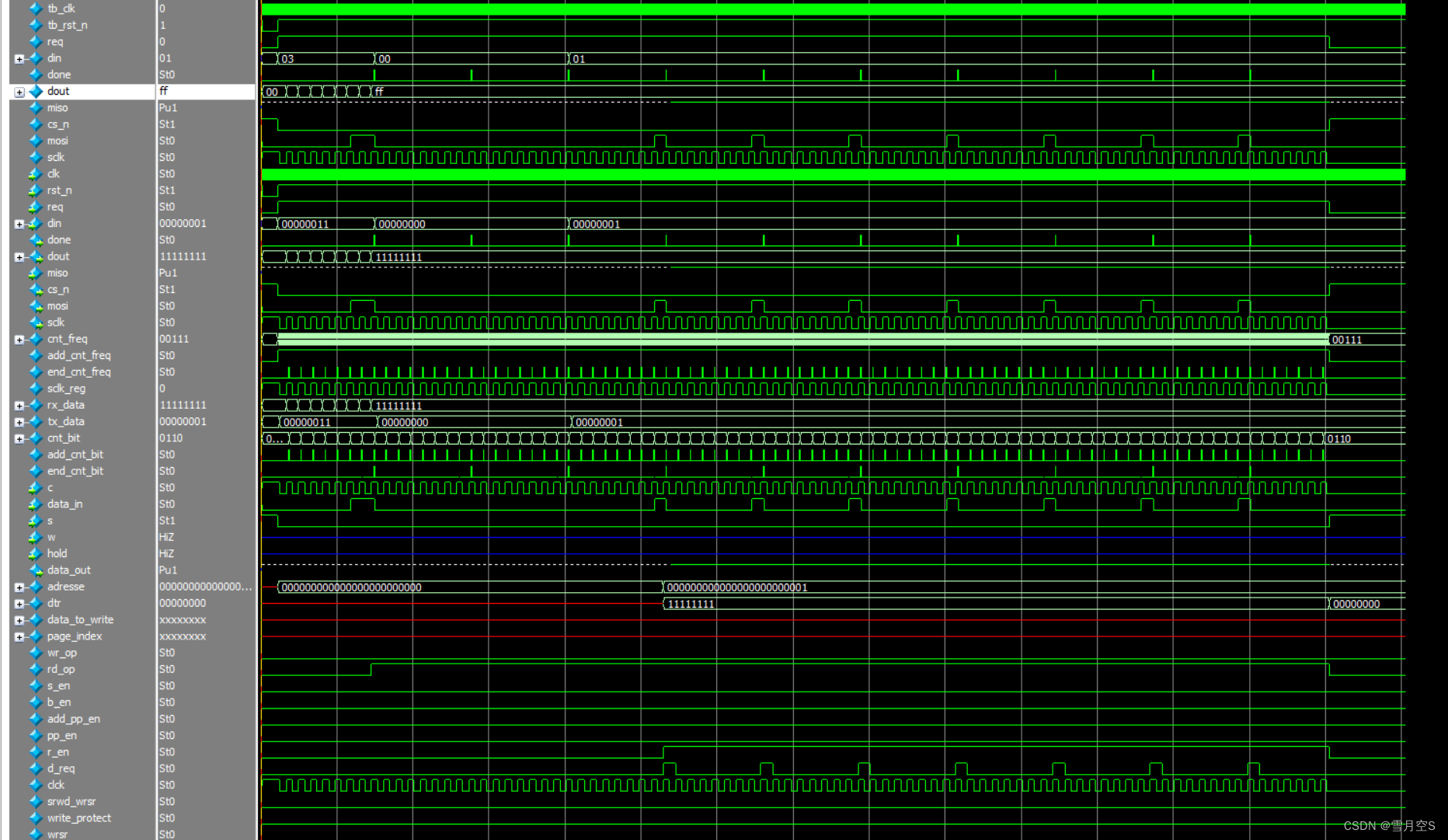
从机初始地址内容全为1,即读出内容为FF


 2019
2019


 被折叠的 条评论
为什么被折叠?
被折叠的 条评论
为什么被折叠?
 到【灌水乐园】发言


