


前一段时间《碧蓝幻想:relink》 发售了,最近没忍住碧瘾 恶狠狠肝了50h+ 到后期死活追击V+因子刷不出来于是就 丨回来继续更新
-------------------------------------
项目名称:简易CPU
预计用时:一下午
资料来源:http://t.csdnimg.cn/Crrtb 作者:IC_Brother
参考教材:夏宇闻《Verilog数字系统设计教程》
书本链接:
链接:https://pan.baidu.com/s/1iFCdPp_gvqyRNtbCxgloBw?pwd=hzt8
提取码:hzt8
--来自百度网盘超级会员V1的分享
date: 2024/02/24 20:50
-------------------------------------
前言:
本人使用的makefile文件代码如下:
使用时一次生成 综合文件和仿真文件列表 以及 testbench列表 和 源代码列表 : make msg
仿真可以用: make cmp
综合暂时没有做
模拟的话就是 make sim
打开Verdi可以用 make verdi
或者综合仿真打开Verdi一步到位: make all
如果有很多需要改进的地方请尽管提,对我个人学习来说,外部反馈十分的宝贵和重要!
## I'm not a professior of makefile , so to use the makefile, you must guarantee that the makefile is at the same directory with the rtl,testbench and timescale
## sorry T.T

CMP_SYN_FILE=CMP_SYN_FILE.txt
RTL=RTL.txt
TB=TB.txt
FILE=file.list
SEED ?= ${shell date +%s}

.PHONY: fls clr rtls tbls all cmp m msg rm_dot verdi sim all

all: msg cmp sim ## make filelist, compile and run sim

m:
    vim ./Makefile  ## open the makefile

msg: rtls tbls fls  ## make the filelist of sources ,testbench and which from compile,synthesis and so on.

clean: msg clr  ## clean the file and filelist created during the design flow

rtls:   ## make the filelist of rtl sources
    find ./ -type f -name '*.v' | grep -v -E '.*[Tt][Bb].*\.v$$'|grep -v -E  'timescale.v'> $(RTL)

tbls:  ## make the filelist of tb
    find ./ -type f -regex '.*[tT][bB]\.\(v\|sv\)$$' > $(TB)

vls:  ## make the filelist of Verilog and SystemVerilog
    find ./ -name "*.sv" > $(FILE)
    find ./ -name "*.v" >> $(FILE)


fls:  ## make the filelist in which is the file created during the design flow
    find ./ -name "*.log" >> $(CMP_SYN_FILE)
    find ./ -name "*.sdf" >> $(CMP_SYN_FILE)
    find ./ -name "*.sdc" >> $(CMP_SYN_FILE)
    find ./ -name "*.svf" >> $(CMP_SYN_FILE)
    find ./ -name "*.vpd" >> $(CMP_SYN_FILE)
    find ./ -name "simv" >> $(CMP_SYN_FILE)
    find ./ -name "csrc" >> $(CMP_SYN_FILE)
    find ./ -name "DVE*" >> $(CMP_SYN_FILE)
    find ./ -name "*key*" >> $(CMP_SYN_FILE)
    find ./ -name "*.fsdb*" >> $(CMP_SYN_FILE)
    find ./ -name "*.rc" >> $(CMP_SYN_FILE)
    find ./ -name "*.conf" >> $(CMP_SYN_FILE)


clr: ## clean the file
    cat ${CMP_SYN_FILE} | xargs rm -rf;
    rm -rf ${RTL};
    rm -rf ${TB};
    rm -rf ${CMP_SYN_FILE};
    rm -rf simv*
    rm -rf *netlist.v
    rm -rf verdiLog
    rm -rf vfastLog

rm_dot: ##clean the dot in the filelist
    sed -i 's/.\///g' ${RTL}
    sed -i 's/.\///g' ${TB}
cmp: ${TB} ${RTL} ##compile the rtl and tb with VCS
    vcs -full64 -sverilog +v2k -debug_acc+all timescale.v ${shell cat RTL.txt} ${shell cat TB.txt} -l com.log -fsdb +define+FSDB

dve:  ##open the dve to see the waveform and run simulation
    dve -vpd *.vpd &

sim:  ## run the rtl simulation
    ./simv -l sim.log

verdi: ## open the Verdi to see the waveform and run simulation
    verdi -f $(FILE) -ssf *.fsdb +nologo &
--------------------------------------------正片开始---------------------------------------------
CPU5个工作阶段
(1)取指(IF,Instruction Fetch),将指令从存储器取出到指令寄存器。每取一条指令,程序计数器自加一。
(2)译指(ID,Instruction Decode),对取出的指令按照规定格式进行拆分和译码。
(3)执行(EX,Execute),执行具体指令操作。
(4)访问存储(MEM,Memory),根据指令访问存储、完成存储和读取。
(5)写回(WB,Write Back),将计算结果写回到存储器。
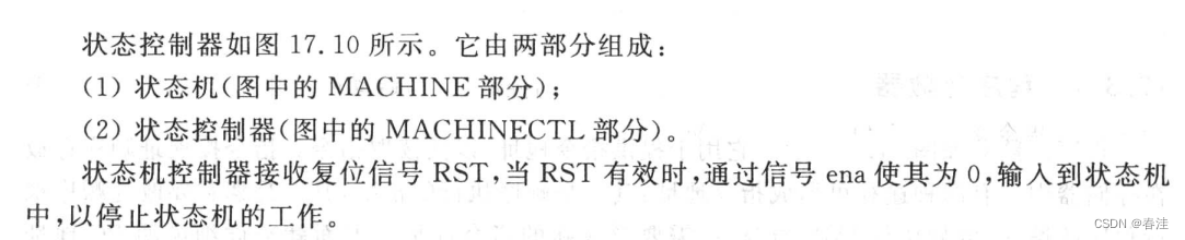
CPU内部结构与Verilog实现
1.ALU算术逻辑运算单元
2.累加器
3.PC(程序计数器)
4.指令寄存器
5.指令解码器
搭配地址MUX锁定存储地址
6.时序和控制相关:
时钟发生器
状态控制器
主状态机
数据控制器
---------------------------------------------
时钟发生器
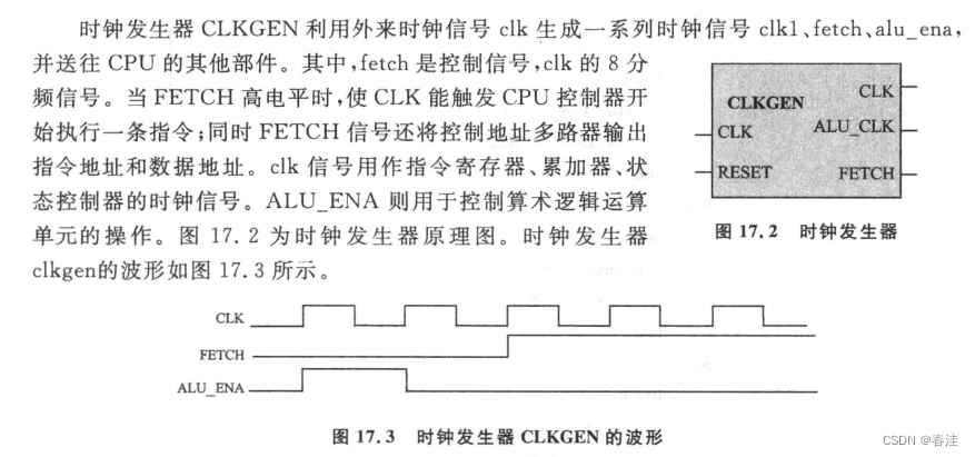
这里ALU使能信号提前于FETCH信号一个周期打开:
是因为计算机执行指令之前需要对指令的操作数进行计算(有时候可能decode也需要)
先把ALU打开确保可以随时接收操作数
---------------------------------------------
我写的代码如下(本质思想是串行移位寄存器):
也可采用书上的源代码
源码:
module clk_gen(
     input clk,
     input reset,
     output fetch,
     output alu_ena
 );

 reg [7:0] shift_reg;

 always @(posedge clk) begin
     if(reset)
             shift_reg <= 8'b00000001;
     else begin
         shift_reg <= {shift_reg[6:0],shift_reg[7]};

     end
 end
assign {fetch,alu_ena} = {shift_reg[4]||shift_reg[5]||shift_reg[6]||shift_reg[7],shift_reg[2]};

endmodule
testbench:
module tb;
reg clk;
reg reset;
wire fetch;
wire ena;
clk_gen gen(
.clk(clk)
,.reset(reset)
,.fetch(fetch)
,.alu_ena(ena)
);
always #10 clk = ~clk;
initial begin
#20
clk = 0;
reset=1;
#100
reset=0;
end
initial begin
$fsdbDumpfile("gen.fsdb");
$fsdbDumpvars(0);
end
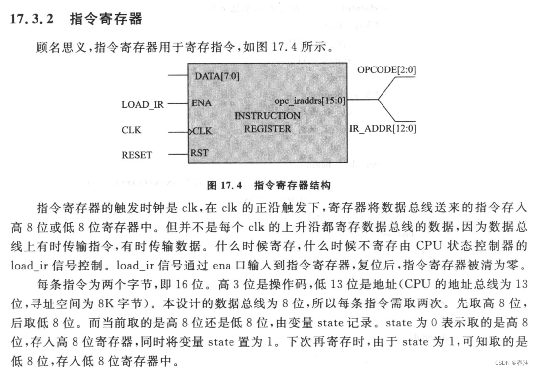
endmodule指令寄存器
指令寄存器主要是用来存来自于RAM/ROM的指令的,他通过接收一个16位指令,来将其分解成后三位的 操作码 和其它13位的 指令地址码。
由于我们的指令寄存器在这里设计的是8bit,所以我们分两次取指,一次高八位,一次低八位。
代码如下:
module ireg(
    input [7:0] ir,
    input en,
    input clk,
    input rst,
    output reg [15:0] opc_iraddr
);

reg state;
always @(posedge clk) begin
    if(rst) begin
            opc_iraddr <= 16'b0;
            state <= 1'b0;
    end
    else begin
            if(en) begin
                casex(state)
                1'b0:   begin
                        opc_iraddr[7:0] <= ir;
                        state <= 1'b1;
                        end
                1'b1:   begin
                        opc_iraddr[15:8] <= ir;
                        state <= 1'b0;
                        end
                default:begin
                        opc_iraddr <= 16'bxxxxxxxxxxxxxxxx;
                        state <= 1'bx;
                        end
                endcase
            end
            else begin
                state <= 1'b0;
            end
    end
end

endmodule
testbench:
module testbench;
reg clk;
reg rst;
reg [7:0] in;
reg ena;
wire [15:0] out;
ireg ir1(
.clk(clk)
,.rst(rst)
,.en(ena)
,.ir(in)
,.opc_iraddr(out)
);
always #20 clk = ~clk;
initial begin
#40
rst = 1;
clk = 0;
ena = 0;
#80
rst=0;
ena = 1;
#20
in = 8'ha1;
#40
in = 8'hb1;
#40
ena = 0;
in = 8'hb2;
#40
in = 8'ha2;
#40
ena = 1;
in = 8'hf1;
#40
in = 8'hf2;
#40
$finish();
end
initial begin
$dumpvars(0);
$dumpfile("reg.fsdb");
end
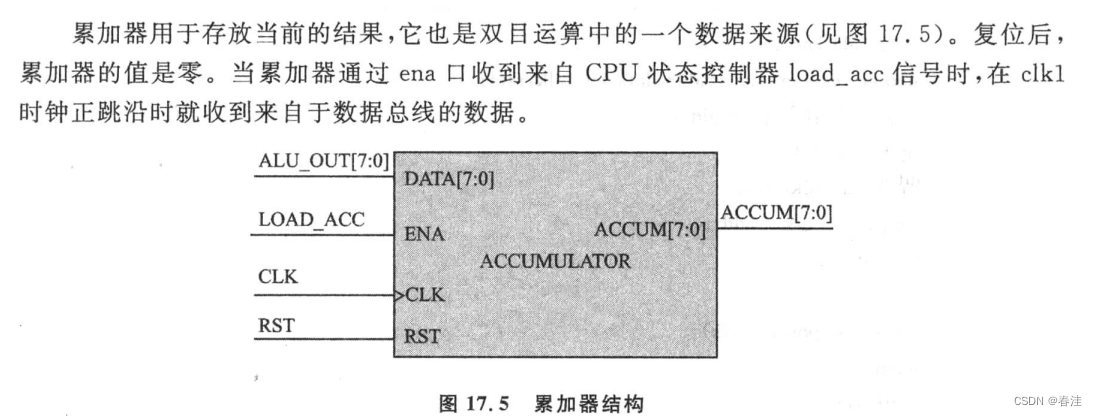
endmodule 累加器
累加器主要是配合ALU和DAT_Controller 一起食用的,他们仨再配合主状态机可以实现一系列指令的执行和数据传输控制操作
代码:
module accumu(
    input [7:0] dat,
    input ena,
    input clk,
    input rst,
    output [7:0] accumu
);
reg [7:0] areg;

always@(posedge clk) begin
    if(rst)
        accumu <= 8'b0;  //reset
    else if(ena)  // cpu 状态控制器发出的 load_acc信号 ,具体可以看总连线图
        accumu <= dat;
end
endmodule
tb就不写了,结构简单,再者比较懒。。。
我就说说意义: 这个累加器其实是一个存放ALU结果的,可能会拿来直接给ALU做积累运算
也可以直接不计算,让它兜转一圈再回到ALU的输出(其实就是跟寄存器一样,俩寄存器打两拍回到原点,在这里的指令集里有这个指令)
总之就是一个根据前3位/后3位的操作码 对后13位/前13位的地址取数并操作的
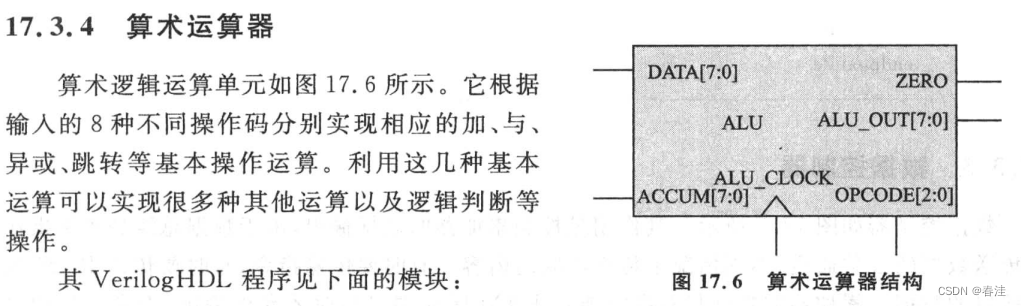
算术运算器
算术运算器同理,配合累加寄存器 + 数据控制器进行指令的执行和数据的发送等操作
需要注意的是,这里的数据输入口一个是累加器一个是直接的来自于data,所以你得先存一个在acc中,再读data,一般你读一个指令的时候,操作数就在指令之中
源码如下:
module alu(
    output [7:0] alu_out,
    output zro,
    input [7:0] dat,
    input [7:0] accum,
    input [2:0] opcode,
    input alu_ena
);

parameter
            HLT     =   3'b000  ,
            SKZ     =   3'b001  ,
            ADD     =   3'b010  ,
            ANDD    =   3'b011  ,
            XORR    =   3'b100  ,
            LDA     =   3'b101  ,
            STO     =   3'b110  ,
            JMP     =   3'b111  ;

    always @(posedge alu_ena) begin //这里的操作码采取的是低3位

            casex(opcode)
                HLT:    alu_out     <=  accum           ;
                SKZ:    alu_out     <=  accum           ;
                ADD:    alu_out     <=  dat + accum     ;
                ANDD:   alu_out     <=  dat & accum     ;
                XORR:   alu_out     <=  dat ^ accum     ;
                LDA :   alu_out     <=  dat             ;
                STO :   alu_out     <=  accum           ;
                JMP :   alu_out     <=  accum           ;
                default: alu_out    <=  8'bxxxx_xxxx    ;
            endcase

    end

    assign zro = !accum;

endmodule
数据控制器
数据控制器也不多说了,配合ALU和ACC做出最后的数据结果输出控制
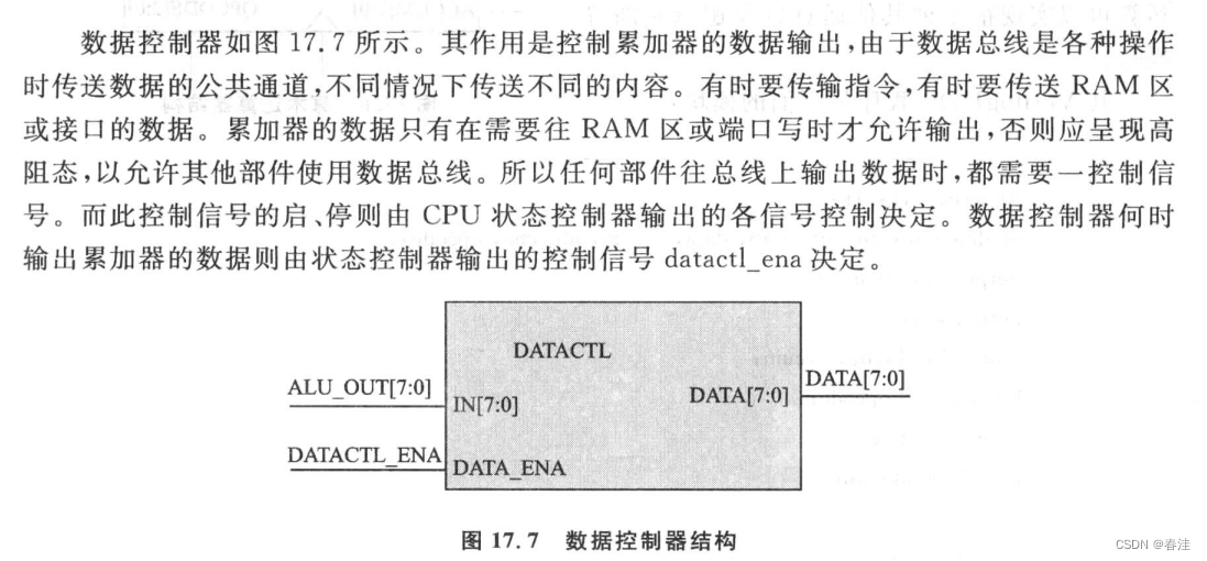
源码如下:(有点像三态门...)
module datactl (
    input   [7:0]       in          ,       // Data input
    input               data_ena    ,       // Data Enable
    output  wire [7:0]  data                // Data output

);

assign  data = (data_ena )? in: 8'bzzzz_zzzz    ;

endmodule
地址多路器
地址多路器的使用主要还是看fetch的来源,这里主要是一个多路复用的结果,省资源一点,因为指令的取指,译码,执行,写回所占的周期都是提前定好的,所以适当控制fetch的生成周期就可以了
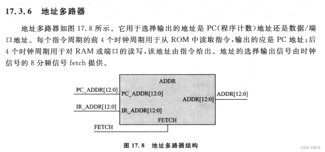
module adr (
    input               fetch       ,   // enable
    input [12:0]        ir_addr     ,   //
    input [12:0]        pc_addr     ,   //
    output wire [12:0]  addr
);


assign  addr = fetch? pc_addr :ir_addr  ;

endmodule
程序计数器
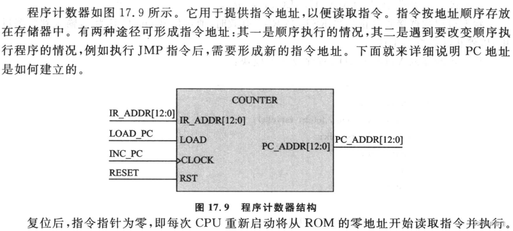
module counter (
    input [12:0]        ir_addr     ,       // program address
    input               load        ,       // Load up signal
    input               clock       ,       // CLock
    input               rst         ,       // Reset
    output  reg [12:0]  pc_addr             // insert program address
);

        always@(posedge clock or posedge rst) begin
                if(rst)
                    pc_addr <= 13'b0_0000_0000_0000;
                else if(load)
                        pc_addr <= ir_addr;
                else
                        pc_addr <= pc_addr + 1;
        end


endmodule
状态机控制器
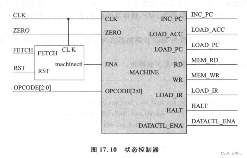
module machinectl (
    input clk           ,       // Clock
    input rst           ,       // Asynchronous reset
    input fetch         ,       // Asynchronous reset active low
    output reg ena              // Enable

);

        always@(posedge clk)begin
                if(rst)
                        ena <= 0;
                else if(fetch)
                        ena <=1;
        end

endmodule
主状态机
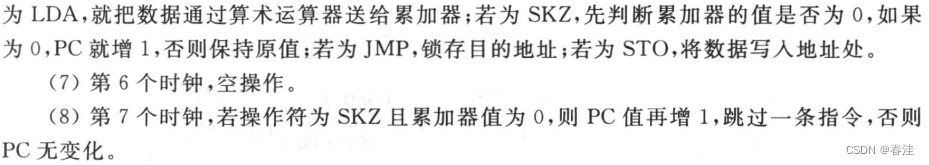
接下来是比较麻烦的地方,这里的指令操作都是根据定义规定好的。所以你暂时需要站在状态控制器的角度去思考一个指令处理的过程
附上主连接图,边看连接图边看代码和定义比较好:(建议窗口看这个,图太大了翻来翻去很麻烦。。。)
源代码:
module machine (
	input 		clk 			,    	// Clock
	input  		ena				, 		// Clock Enable
	input 		zero			,  		//
	input [2:0]	opcode 			,		// OP code
	output 	reg inc_pc 			,		//
	output  reg load_acc		, 		//
	output	reg	load_pc 		, 		//
	output 	reg rd 				,		//
	output 	reg wr 				, 		//
	output 	reg load_ir 		, 		//
	output 	reg datactl_ena 	, 		//
	output  reg halt
);

	reg  [2:0] state  ;
//parameter
		parameter
					HLT 	= 3'b000	,
					SKZ 	= 3'b001	,
					ADD 	= 3'b010	,
					ANDD 	= 3'b011	,
					XORR 	= 3'b100	,
					LDA 	= 3'b101	,
					STO 	= 3'b110	,
					JMP 	= 3'b111	;
		always@(negedge clk) begin
				if(!ena)  //收到复位信号rst,进行复位操作
					begin
						state <= 3'b000;
						{inc_pc,load_acc,load_pc,rd} <= 4'b0000;
						{wr,load_ir,datactl_ena,halt} <= 4'b0000;
					end
				else
					ctl_cycle;
		end

			//------- task ctl_cycle -------

			task ctl_cycle;
				begin
					casex(state)
						3'b000:   //load high 8bits in struction
								begin
									{inc_pc,load_acc,load_pc,rd} <= 4'b0001;
									{wr,load_ir,datactl_ena,halt} <= 4'b0100;
									state <= 3'b001;
								end
						3'b001://pc increased by one then load low 8bits instruction
								begin
									{inc_pc,load_acc,load_pc,rd} <= 4'b1001;
									{wr,load_ir,datactl_ena,halt} <= 4'b0100;
									state <= 3'b010;
								end
						3'b010: //idle
								begin
									{inc_pc,load_acc,load_pc,rd} <= 4'b0000;
									{wr,load_ir,datactl_ena,halt} <= 4'b0000;
									state <= 3'b011;
								end
						3'b011:  //next instruction address setup 分析指令开始点
								begin
									if(opcode == HLT)//指令为暂停HLT
										begin
											{inc_pc,load_acc,load_pc,rd} <= 4'b1000;
											{wr,load_ir,datactl_ena,halt} <= 4'b0001;
										end
									else
										begin
											{inc_pc,load_acc,load_pc,rd} <= 4'b1000;
											{wr,load_ir,datactl_ena,halt} <= 4'b0000;
										end
								state <= 3'b100;
								end
						3'b100: //fetch oprand
								begin
									if(opcode == JMP)
										begin
											{inc_pc,load_acc,load_pc,rd} <= 4'b0010;
											{wr,load_ir,datactl_ena,halt} <= 4'b0000;
										end
									else if(opcode == ADD || opcode == ANDD || opcode == XORR || opcode == LDA)
											begin
												{inc_pc,load_acc,load_pc,rd} <= 4'b0001;
												{wr,load_ir,datactl_ena,halt} <= 4'b0000;

											end
									else if(opcode == STO)
											begin
												{inc_pc,load_acc,load_pc,rd} <= 4'b0000;
												{wr,load_ir,datactl_ena,halt} <= 4'b0010;
											end
									else
										begin
												{inc_pc,load_acc,load_pc,rd} <= 4'b0000;
												{wr,load_ir,datactl_ena,halt} <= 4'b0000;
										end
									state <= 3'b101;
								end
						3'b101://operation
								begin
									if(opcode == ADD || opcode == ANDD ||opcode ==XORR ||opcode == LDA)//过一个时钟后与累加器的内存进行运算
										begin
												{inc_pc,load_acc,load_pc,rd} <= 4'b0101;
												{wr,load_ir,datactl_ena,halt} <= 4'b0000;
										end
									else if(opcode == SKZ && zero == 1)// & and &&
											begin
												{inc_pc,load_acc,load_pc,rd} <= 4'b1000;
												{wr,load_ir,datactl_ena,halt} <= 4'b0000;
											end
										else if(opcode == JMP)
												begin
													{inc_pc,load_acc,load_pc,rd} <= 4'b1010;
													{wr,load_ir,datactl_ena,halt} <= 4'b0000;
												end
										else if(opcode == STO)
													begin//过一个时钟后把wr变为1,写到RAM中
														{inc_pc,load_acc,load_pc,rd} <= 4'b0000;
														{wr,load_ir,datactl_ena,halt} <= 4'b1010;
													end
										else
												begin
														{inc_pc,load_acc,load_pc,rd} <= 4'b0000;
														{wr,load_ir,datactl_ena,halt} <= 4'b0000;
												end
										state <= 3'b110;
								end
						3'b110:
									begin
										if(opcode == STO)
											begin
												{inc_pc,load_acc,load_pc,rd} <= 4'b0000;
												{wr,load_ir,datactl_ena,halt} <= 4'b0010;
											end
										else if(opcode == ADD || opcode == ANDD || opcode == XORR || opcode == LDA)
												begin
													{inc_pc,load_acc,load_pc,rd} <= 4'b0001;
													{wr,load_ir,datactl_ena,halt} <= 4'b0000;
												end
										else
												begin
													{inc_pc,load_acc,load_pc,rd} <= 4'b0000;
													{wr,load_ir,datactl_ena,halt} <= 4'b0000;
												end
									state <= 3'b111;
									end
						3'b111:
								begin
									if(opcode == SKZ && zero == 1)
										begin
											{inc_pc,load_acc,load_pc,rd} <= 4'b1000;
											{wr,load_ir,datactl_ena,halt} <= 4'b0000;
										end
									else
										begin
											{inc_pc,load_acc,load_pc,rd} <= 4'b0000;
											{wr,load_ir,datactl_ena,halt} <= 4'b0000;
										end
								state <= 3'b000;
								end
						default:
									begin
										{inc_pc,load_acc,load_pc,rd} <= 4'b0000;
										{wr,load_ir,datactl_ena,halt} <= 4'b0000;
										state <= 3'b000;
									end
					endcase
				end
			endtask

endmodule
执行表述:


 7254
7254


 被折叠的 条评论
为什么被折叠?
被折叠的 条评论
为什么被折叠?
 到【灌水乐园】发言


