


今天刚开学,于是晚点更新
上一节做了一个简单的CPU,这次来设计外围电路进行验证测试
------------------------正文分割线--------------------------------
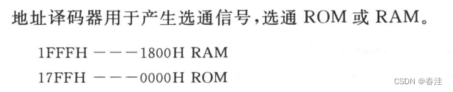
地址译码器
光设计一个CPU是没有什么用处的,需要搭配外来的数据才能验证其正确性
所以我们需要一个存取数据的RAM 和 用来 读取指令 的 ROM
CPU的地址属于是虚拟地址,外接的RAM/ROM是实际物理地址,需要有地址译码器来选通和通信
规则如下:
源代码:
module addr_decode(
    input [12:0]addr,
    output reg  rom_sel,
    output reg ram_sel
);

always @(*) begin
    casex(addr)
    13'b1_1xxx_xxxx_xxxx: {rom_sel,ram_sel} <= 2'b01;
    13'b1_0xxx_xxxx_xxxx: {rom_sel,ram_sel} <= 2'b10;
    13'b0_xxxx_xxxx_xxxx: {rom_sel,ram_sel} <= 2'b10;
    default: {rom_sel,ram_sel} <= 2'b00;
    endcase
end

endmodule
RAM & ROM
这个没什么好说的,不是很难:
RAM源代码:
module ram(
    input ena,
    input rd,
    input wr,
    inout wire [7:0] dat,
    input [9:0] addr
);

reg [7:0] ram[10'h3ff:0];

assign dat = (rd&&ena)?ram[addr]:8'hzz;

always @(posedge wr) begin
    ram[addr] <= dat;
end

endmodule
ROM源代码:
module rom(
input ena,
input rd,
input [9:0] addr,
output [7:0] ir_dat
);
reg [7:0] rom [13'h1ff:0];
assign ir_dat = (rd&&ena)? rom[addr]:8'hzz;
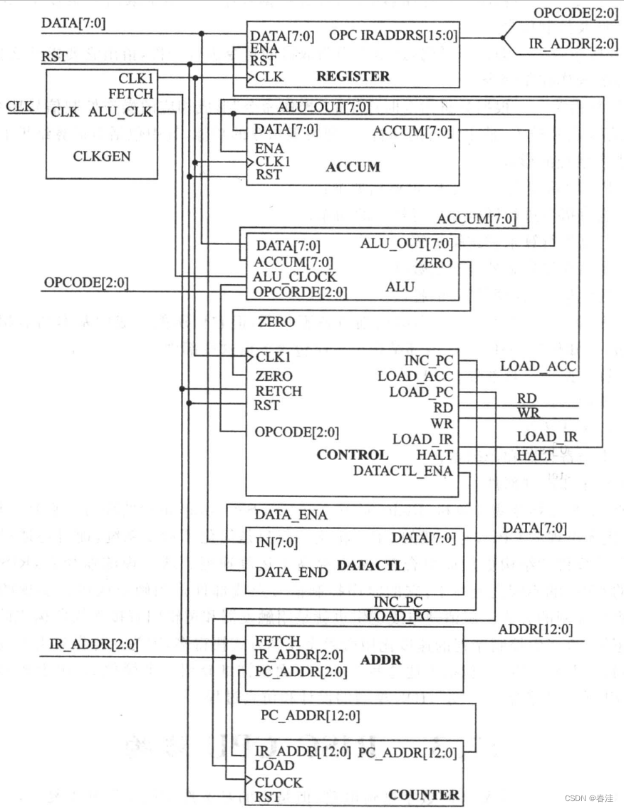
endmodule将各个模块链接起来
根据主状态机那里给出的链接形式开始连接:
源代码如下:
module top(
    input clk,
    input rst,
    output rd,
    output wr,
    output halt,
    output fetch,

    output [12:0]addr,
    output [12:0]ir_addr,
    output [12:0]pc_addr,
    inout [7:0] data,

    output wire [2:0] opcode
);

    wire [7:0] alu_out;
    wire [7:0] accum;

    wire zero  ;
    wire inc_pc ;
    wire load_acc ;
    wire loac_pc ;
    wire load_ir ;
    wire dat_ena ;
    wire ctr_ena ;
    wire alu_ena ;

    clk_gen mclkgen(
        .clk(clk)
       ,.reset(rst)
       ,.fetch(fetch)
       ,.alu_ena(alu_ena)
       );

    ireg regm(
        .ir(data)
       ,.en(ena)
       ,.clk(clk)
       ,.rst(rst)
       ,.opc_iraddr({opcode,ir_addr})
    );

    accumu acc1(
        .dat(alu_out)
       ,.ena(load_acc)
       ,.clk(clk)
       ,.rst(rst)
       ,.accumu(accum)
    );

    alu alu1(
        .alu_clk(clk)
        ,.accum(accum)
        ,.opcode(opcode)
        ,.dat(data)
        ,.alu_out(alu_out)
        ,.zro(zero)
    );

   machinectl m_ctrl(
        .clk(clk)
        ,.rst(rst)
        ,.fetch(fetch)
        ,.ena(ctr_ena)
   );

   machine mac1(
        .clk(clk)
        ,.ena(ctr_ena)
        ,.zero(zero)
        ,.opcode(opcode)
        ,.inc_pc(inc_pc)
        ,.load_acc(load_acc)
        ,.load_pc(load_pc)
        ,.rd(rd)
        ,.wr(wr)
        ,.load_ir(load_ir)
        ,.datactl_ena(dat_ena)
        ,.halt(fetch)
   );

   datactl dat_ctrl(
        .in(alu_out)
       ,.data_ena(dat_ena)
       ,.data(data)
   );

   adr addr_mux1(
        .fetch(fetch)
        ,.ir_addr(ir_addr)
        ,.pc_addr(pc_addr)
        ,.addr(addr)
   );

   counter pc(
        .ir_addr(ir_addr)
        ,.load(load_pc)
        ,.clock(inc_pc)
        ,.rst(rst)
        ,.pc_addr(pc_addr)
   );

endmodule
针对CPU测试,采用汇编程序和RAM/ROM读取数据的形式进行验证:
tb文件:
注意修改test*.pro 和 test*.dat的路径
`timescale 1ns/1ns

`define PERIOD 100 // matches clk_gen.v

module cputop;
  reg [( 3 * 8 ): 0 ] mnemonic; // array that holds 3 8 bits ASCII characters
  reg  [ 12 : 0 ] PC_addr, IR_addr;
  reg  reset_req, clock;
  wire [ 12 : 0 ] ir_addr, pc_addr; // for post simulation.
  wire [ 12 : 0 ] addr;
  wire [  7 : 0 ] data;
  wire [  2 : 0 ] opcode;           // for post simulation.
  wire fetch;                       // for post simulation.
  wire rd, wr, halt, ram_sel, rom_sel;
  integer test;

  //-----------------DIGITAL LOGIC----------------------
  top t_cpu (.clk( clock ),.rst( reset_req ),.halt( halt ),.rd( rd ),.wr( wr ),.addr( addr ),.data( data ),.opcode( opcode ),.fetch( fetch ),.ir_addr( ir_addr ),.pc_addr( pc_addr ));
  ram t_ram (.addr ( addr [ 9 : 0 ]),.rd ( rd ),.wr ( wr ),.ena ( ram_sel ),.dat ( data ));
  rom t_rom (.addr ( addr          ),.rd ( rd ),              .ena ( rom_sel ),.ir_dat ( data ));
  addr_decode t_addr_decoder (.addr( addr ),.ram_sel( ram_sel ),.rom_sel( rom_sel ));

  //-------------------SIMULATION-------------------------
  initial begin
    clock = 0;
    // display time in nanoseconds
    $timeformat ( -9, 1, "ns", 12 );
    display_debug_message;
    sys_reset;
    test1; $stop;
    test2; $stop;
    test3;
    $finish; // simulation is finished here.
  end // initial

  task display_debug_message;
    begin
      $display ("\n************************************************"  );
      $display (  "* THE FOLLOWING DEBUG TASK ARE AVAILABLE:      *"  );
      $display (  "* \"test1;\" to load the 1st diagnostic program. *");
      $display (  "* \"test2;\" to load the 2nd diagnostic program. *");
      $display (  "* \"test3;\" to load the     Fibonacci  program. *");
      $display (  "************************************************\n");
    end
  endtask // display_debug_message

  task test1;
    begin
      test = 0;
      disable MONITOR;
      $readmemb ("../test1/test1.pro", t_rom.rom );
      $display ("rom loaded successfully!");
      $readmemb ("../test1/test1.dat", t_ram.ram );
      $display ("ram loaded successfully!");
      #1 test = 1;
      #14800;
      sys_reset;
    end
  endtask // test1

  task test2;
    begin
      test = 0;
      disable MONITOR;
      $readmemb ("../test2/test2.pro", t_rom.rom );
      $display ("rom loaded successfully!");
      $readmemb ("../test2/test2.dat", t_ram.ram );
      $display ("ram loaded successfully!");
      #1 test = 2;
      #11600;
      sys_reset;
    end
  endtask // test2

  task test3;
    begin
      test = 0;
      disable MONITOR;
      $readmemb ("../test3/test3.pro", t_rom.rom );
      $display ("rom loaded successfully!");
      $readmemb ("../test3/test3.dat", t_ram.ram );
      $display ("ram loaded successfully!");
      #1 test = 3;
      #94000;
      sys_reset;
    end
  endtask // test1

  task sys_reset;
    begin
      reset_req = 0;
      #( `PERIOD * 0.7 ) reset_req = 1;
      #( 1.5 * `PERIOD ) reset_req = 0;
    end
  endtask // sys_reset

  //--------------------------MONITOR--------------------------------
  always@( test ) begin: MONITOR
    case( test )
      1: begin // display results when running test 1
        $display("\n*** RUNNING CPU test 1 - The Basic CPU Diagnostic Program ***");
        $display("\n        TIME      PC      INSTR      ADDR      DATA          ");
        $display("         ------    ----    -------    ------    ------         ");
        while( test == 1 )@( t_cpu.pc_addr ) begin // fixed
          if(( t_cpu.pc_addr % 2 == 1 )&&( t_cpu.fetch == 1 )) begin // fixed
            #60  PC_addr <= t_cpu.pc_addr - 1;
                 IR_addr <= t_cpu.ir_addr;
            #340 $strobe("%t %h %s %h %h", $time, PC_addr, mnemonic, IR_addr, data ); // Here data has been changed t_cpu.m_register.data
          end // if t_cpu.pc_addr % 2 == 1 && t_cpu.fetch == 1
        end // while test == 1 @ t_cpu.pc_addr
      end

      2: begin // display results when running test 2
        $display("\n*** RUNNING CPU test 2 - The Basic CPU Diagnostic Program ***");
        $display("\n        TIME      PC      INSTR      ADDR      DATA          ");
        $display("         ------    ----    -------    ------    ------         ");
        while( test == 2 )@( t_cpu.pc_addr ) begin // fixed
          if(( t_cpu.pc_addr % 2 == 1 )&&( t_cpu.fetch == 1 )) begin // fixed
            #60  PC_addr <= t_cpu.pc_addr - 1;
                 IR_addr <= t_cpu.ir_addr;
            #340 $strobe("%t %h %s %h %h", $time, PC_addr, mnemonic, IR_addr, data ); // Here data has been changed t_cpu.m_register.data
          end // if t_cpu.pc_addr % 2 == 1 && t_cpu.fetch == 1
        end // while test == 2 @ t_cpu.pc_addr
      end

      3: begin // display results when running test 3
        $display("\n*** RUNNING CPU test 3 - An Executable Program **************");
        $display("***** This program should calculate the fibonacci *************");
        $display("\n        TIME      FIBONACCI NUMBER          ");
        $display("         ------    -----------------_         ");
        while( test == 3 ) begin
          wait( t_cpu.opcode == 3'h 1 ) // display Fib. No. at end of program loop
          $strobe("%t     %d", $time, t_ram.ram [ 10'h 2 ]);
          wait( t_cpu.opcode != 3'h 1 );
        end // while test == 3
      end
    endcase // test
  end // MONITOR: always@ test

  //-------------------------HALT-------------------------------
  always@( posedge halt ) begin // STOP when HALT intruction decoded
    #500 $display("\n******************************************");
         $display(  "** A HALT INSTRUCTION WAS PROCESSED !!! **");
         $display(  "******************************************");
  end // always@ posedge halt

  //-----------------------CLOCK & MNEMONIC-------------------------
  always#(`PERIOD / 2 ) clock = ~ clock;

  always@( t_cpu.opcode ) begin // get an ASCII mnemonic for each opcode
    case( t_cpu.opcode )
      3'b 000 : mnemonic = "HLT";
      3'b 001 : mnemonic = "SKZ";
      3'b 010 : mnemonic = "ADD";
      3'b 011 : mnemonic = "AND";
      3'b 100 : mnemonic = "XOR";
      3'b 101 : mnemonic = "LDA";
      3'b 110 : mnemonic = "STO";
      3'b 111 : mnemonic = "JMP";
      default : mnemonic = "???";
    endcase
  end
endmodule
相关汇编文件链接:
http://t.csdnimg.cn/rBGYR 在VIVADO上实现的非常简易的RISC-V CPU设计(来自《Verilog数字系统设计》夏宇闻著)作者:Jefferymeng


 373
373


 被折叠的 条评论
为什么被折叠?
被折叠的 条评论
为什么被折叠?
 到【灌水乐园】发言


