


 16-Bit SAR ADC, Single Supply, 4-20mA Acquisition System
https://github.com/AntiFailsafe/4-20mA_Acquisition_System
https://gitee.com/chinghsien/4-20mA_Acquisition_System
Words from author
This system was developed during my time in UESTC (University of Electronic Science and Technology of China) robotic team-LIMITI for Robocon 2022 of mainland China and Team China for ABU Robocon 2022. My future research will be no longer focusing on board level circuits. As a commemoration of the past year, I open source this circuit and it is suitable for majority of 4-20mA sensors, not just DT35. I hope it will be helpful to you. Good luck!
Introduction
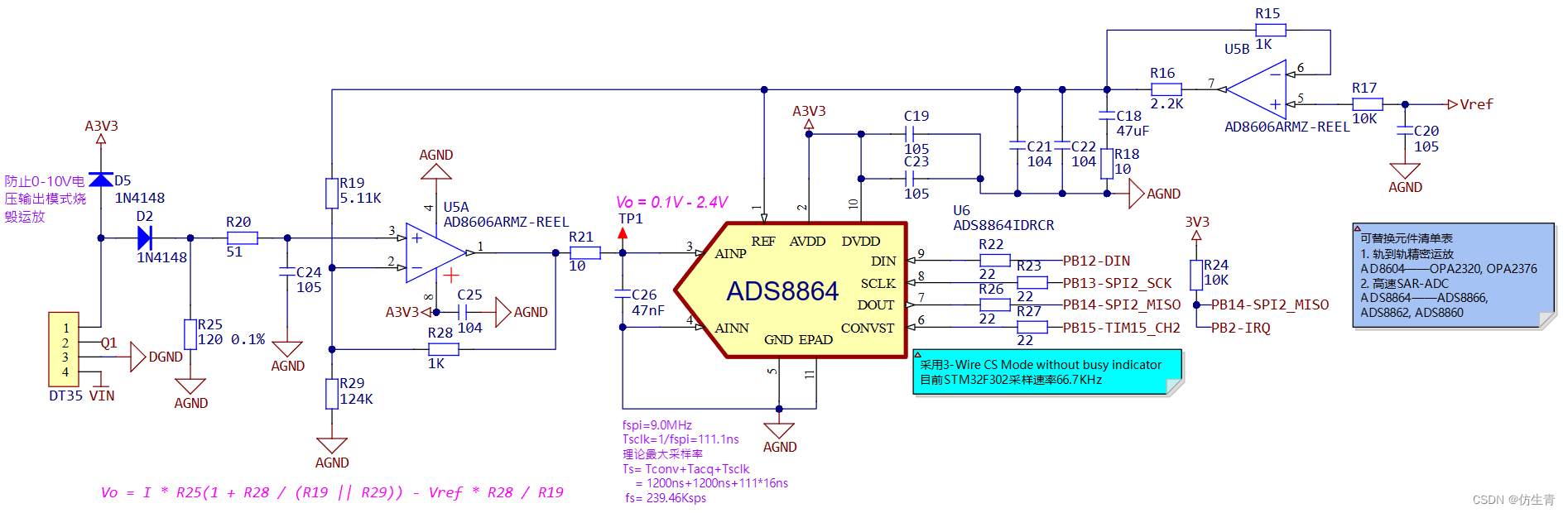
This system incorporates ADS8864 and STM32F302C8T6 to processes 4 mA to 20 mA input signals using a single 24V DC supply. The total error before room temperature calibration is ±4 LSBs, namely ±0.06% FSR at the room temperature (27°C).
The sensor employed in this system is Sick’s DT35, but input terminal could be modified to meet a wide variety of industrial measurements.
Circuit description
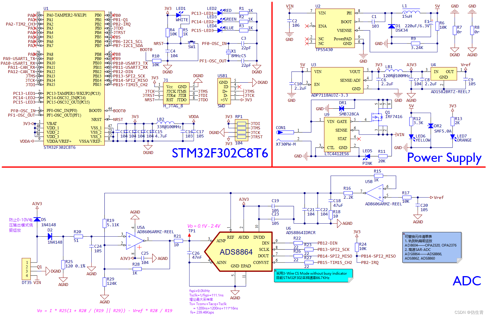
The circuit is comprised of a level shifting circuit, an input current-to-voltage converter, an ADC stage, and an output digital signal processing stage. Resistor R 25 R_{25} R25 converts the 4 mA to 20 mA input signal into a voltage. The level shifting circuit’s input voltage ranges from 0.48 V to 2.4 V when R 25 = 120 Ω R_{25} = 120 \ \Omega R25=120 Ω and the input current is between 4 and 20 mA. While diode D1 is used to limit the input voltage for incorrect input of voltage instead of current, diode D2 is used to protect against an inadvertent reverse connection of the input current source.
The U5A op amp, which is 1 2 {\frac 1 2} 21 of the dual AD8606, level shifts and attenuates the voltage across R25. With 100 mV headroom to ensure linearity, the op amp’s output range of 0.1 V to 2.4 V matches the input range of the ADC (0 V to 2.5 V). The necessary offset is produced using the remaining AD1582’s buffered voltage reference (VREF = 2.5 V).
The minimum output voltage (low limit of the range) is set to 100 mV to provide a safety margin while taking into account the tolerances of the parts. To provide 100 mV of headroom for the positive swing at the ADC input, the maximum limit of the output range is set at 2.4 V. As a result, the op amp’s nominal output voltage range is 0.1 V to 2.4 V. The second half of the AD8606 (U5B) is used to buffer the 2.5 V voltage reference of the ADS8864 (U6) ADC.
Due to its low offset voltage (65 μV maximum), low bias current (1 pA maximum), and low noise (12 nV/√Hz maximum), the AD8606 is selected for this application. With a 3.3 V supply, there is just 9.2 mW of power dissipation. Additionally, other opamps can be used. The replacements could be OPA2320, OPA2376, and other options, as shown in the Figure above.
The op amp output stage is followed by a single-pole RC filter (R21/C26) to help reduce out-of-band noise. The RC filter’s cutoff frequency is set to 339 kHz. To further lower the filter cutoff frequency in the occurrence of low frequency industrial noise, an extra filter (R20/C24) can be installed. In this situation, the ADS8864’s sampling rate might be lowered due to the narrower signal bandwidth.
Its ultralow power of 0.65mW at 100-kSPS led to the selection of the ADS8864 (U6) 16-bit 400-kSPS SAR ADC. SPI is compatible with its high-speed serial interface. The DSP core, STM32F302C8T6, which is the system’s sampling rate limiter, has set the Nyquist rate to 66.6 KHz.
Circuit Design
The low-frequency transfer function is obtained from the superposition principle.
V o u t = I i n R 25 ( 1 + R 28 R 19 ∣ ∣ R 29 ) − V r e f R 28 R 19 V_{out}=I_{in} R_{25} (1+ \frac {R_{28}} {R_{19} ||R_{29}} )-V_{ref} \frac {R_{28}} {R_{19}} Vout=IinR25(1+R19∣∣R29R28)−VrefR19R28
where,
I i n = 4 m A t o 20 m A I_{in} = 4\ mA\ to\ 20\ mA Iin=4 mA to 20 mA
R 19 ∣ ∣ R 29 = R 19 R 29 R 19 + R 29 R_{19} ||R_{29}= \frac {R_{19} R_{29}} {R_{19}+R_{29}} R19∣∣R29=R19+R29R19R29
The low-frequency gain of the circuit is:
G = Δ V o u t Δ I i n = R 25 ( 1 + R 28 R 19 ∣ ∣ R 29 ) = ( 2.4 − 0.1 ) V ( 20 − 4 ) m A G= \frac {ΔV_{out}} {ΔI_{in}} = R_{25} (1+ \frac {R_{28}} {R_{19} ||R_{29}} )= \frac {(2.4-0.1)V} {(20-4 )mA } G=ΔIinΔVout=R25(1+R19∣∣R29
 最低0.47元/天 解锁文章


 1万+
1万+


 被折叠的 条评论
为什么被折叠?
被折叠的 条评论
为什么被折叠?
 到【灌水乐园】发言


