


Lecture12 | Single-Cycle CPU Datapath
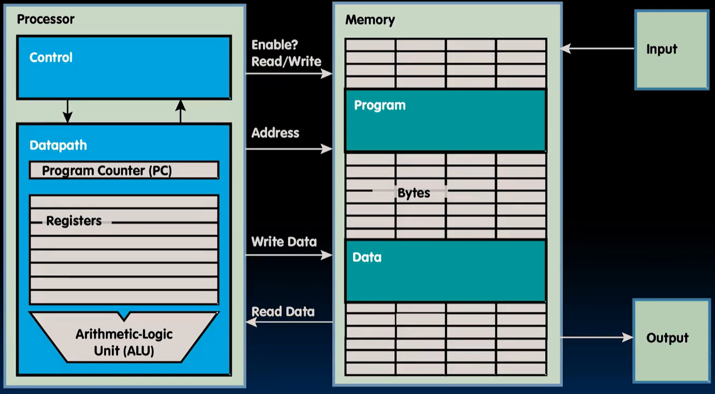 ## The CPU Processor(CPU): the active part of the computer that does all the work(data manipulation and decision-making).
CPU contains two parts, which are the data path and the control.
Datapath
portion of the processor that contains hardware necessary to perform operations required by the processor.
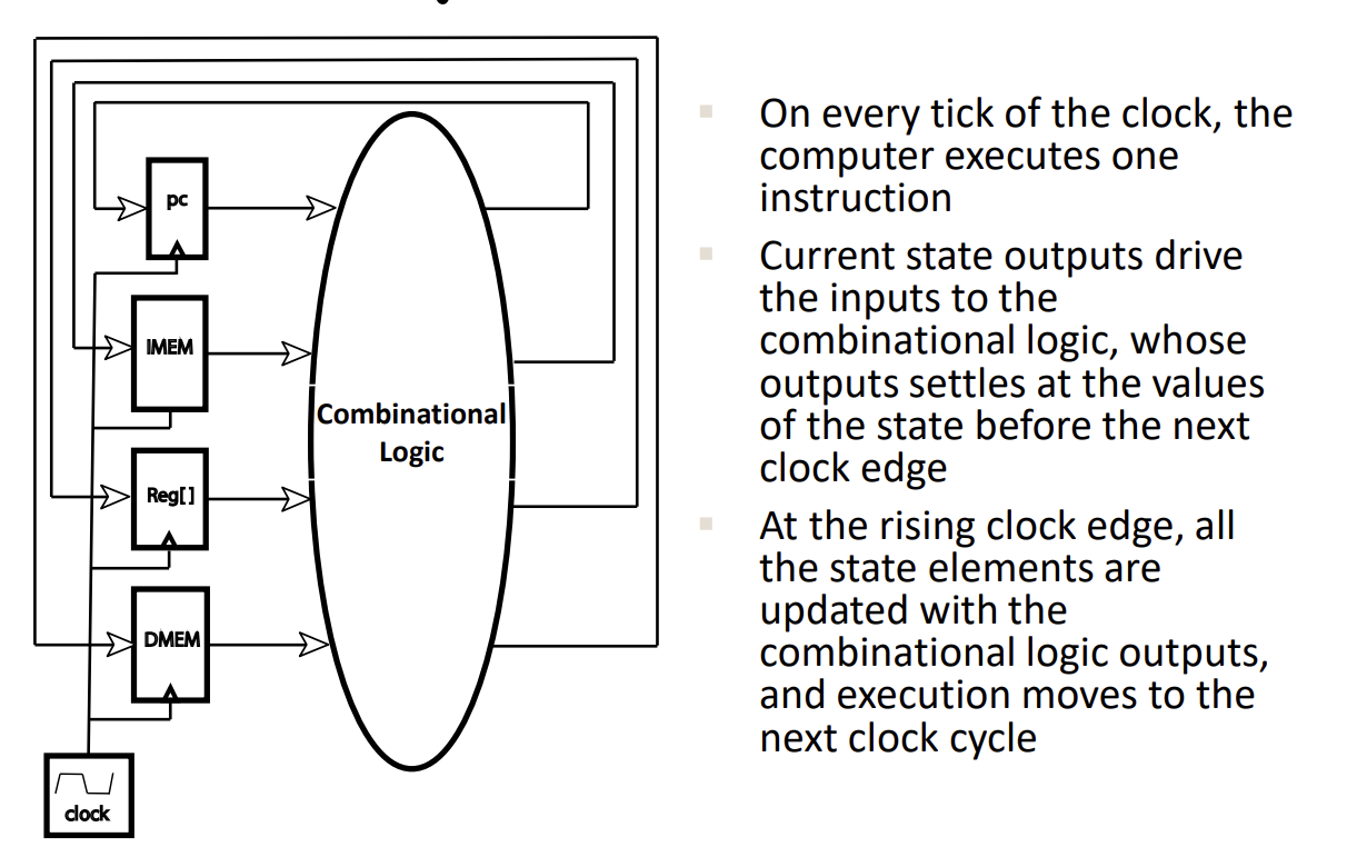
One-Instruction-Per-Cycle RISC-V Machine
Five Stages of the Datapath
- Instruction Fetch(IF) 指令获取
- Instruction Decode(ID) 指令解码
- Execute(EX) - ALU 执行
- Memory Access(MEM) 内存访问
- Write Back to Register(WB) 写回寄存器
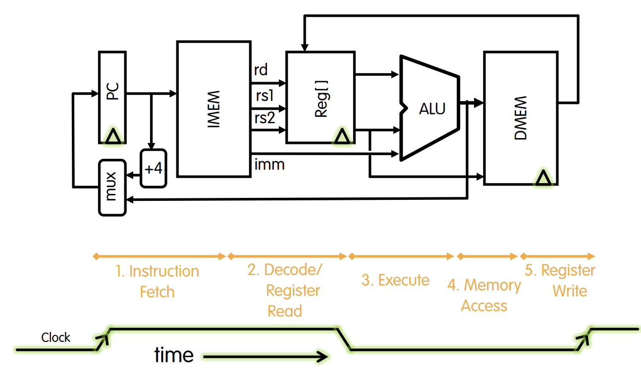
The program counter(PC), when it is executing instructions in sequence, will be incremented by 4 bytes to point to the next 32-bit word in RISC-V. The MUX here is to bypass that increment and write a branch target if the branch is to be taken. In that way, the program counter would be pointing to the instruction where the branch lands.
We are going to start instruction execution on the first rising edge of a clock with the instruction fetch. And we are going to write back the final result on the next rising edge of a clock. So at that point, the registers will be updated, and the program counter will be updated to contain the new address of the next instruction to be fetched.
Datapath Components

首先肯定需要的就是寄存器,
Register
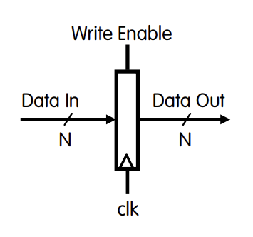
A 32-bit register will consist of 32 filp-flops, and they’re all going to be written together on a rising edge of a clock.
- Low(or deasserted) (0): Data Out will not change
- Asserted(1): Data Out will become Data In on positive edge of clock
Register file(regfile, RF)
RF consists of 32 registers.
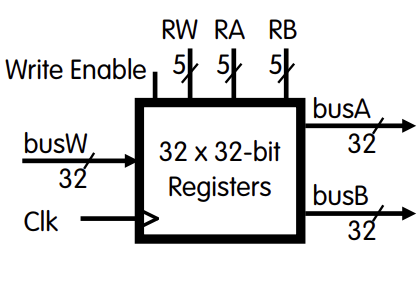
- Two 32-bit output busses: busA and busB
- One 32-bit input bus: busW
- RA(number) selects the register to put on busA(data)
- RB(number) selects the register to put on busB(data)
- RW(number) selects the register to be written via busW(data) when Write Enable is 1
- Clk input is a factor ONLY during write operation
- During read operation, behaves as a combinational logic block:
- RA or RB valid -> busA or busB valid after “access time”
只需要时钟来写入,而不需要时钟来读取寄存器文件,只要我们将 RA 和 RB 值放在器输入端,即地址输入端,输出就会出现,这些输出出现之前会有一些延迟,也就是访问时间(access time)。
- RA or RB valid -> busA or busB valid after “access time”
Memory
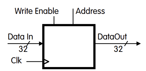 - One input bus: Data In - One output bus: Data Out - For Read: Address selects the word to put on Data Out - For Write: Set Write Enable = 1: address selects the memory word to be written via the Data In bus - CLK input is a factor ONLY during write operation - During read operation, behaves as a combinational logic block - Address valid -> Data Out valid after "access time"
When we put an address here and don’t clock it, the data will magically that corresponds to that address, show up at the data outputs.
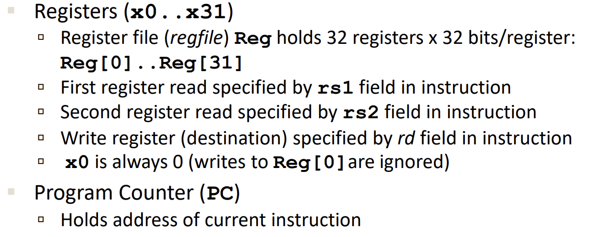
State Required by RV32I ISA
每条指令在执行过程中都会读取和更新三组元素状态:寄存器、程序计数器和内存

R-Type Add Datapath
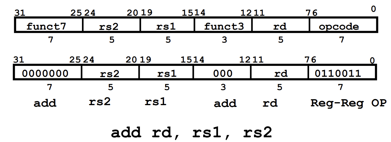
指令导致机器状态的两项变化:
- R e g [ r d ] = R e g [ r s 1 ] + R e g [ r s 2 ] Reg[rd] = Reg[rs1] + Reg[rs2] Reg[rd]=Reg[rs1]+Reg[rs2]
- P C = P C + 4 PC = PC + 4 PC=PC+4
Datapath for add
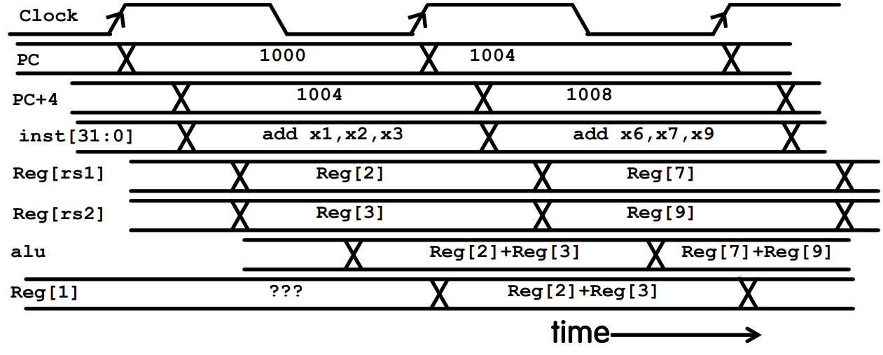
 ### Timing Diagram for add
 对于 sub,只需要改变 ALU 部分,ALUSel(add = 0 / sub = 1) $Reg[rd] = Reg[rs1]~ ~+ / -~ ~Reg[rs2]$ ## Datapath With Immediates
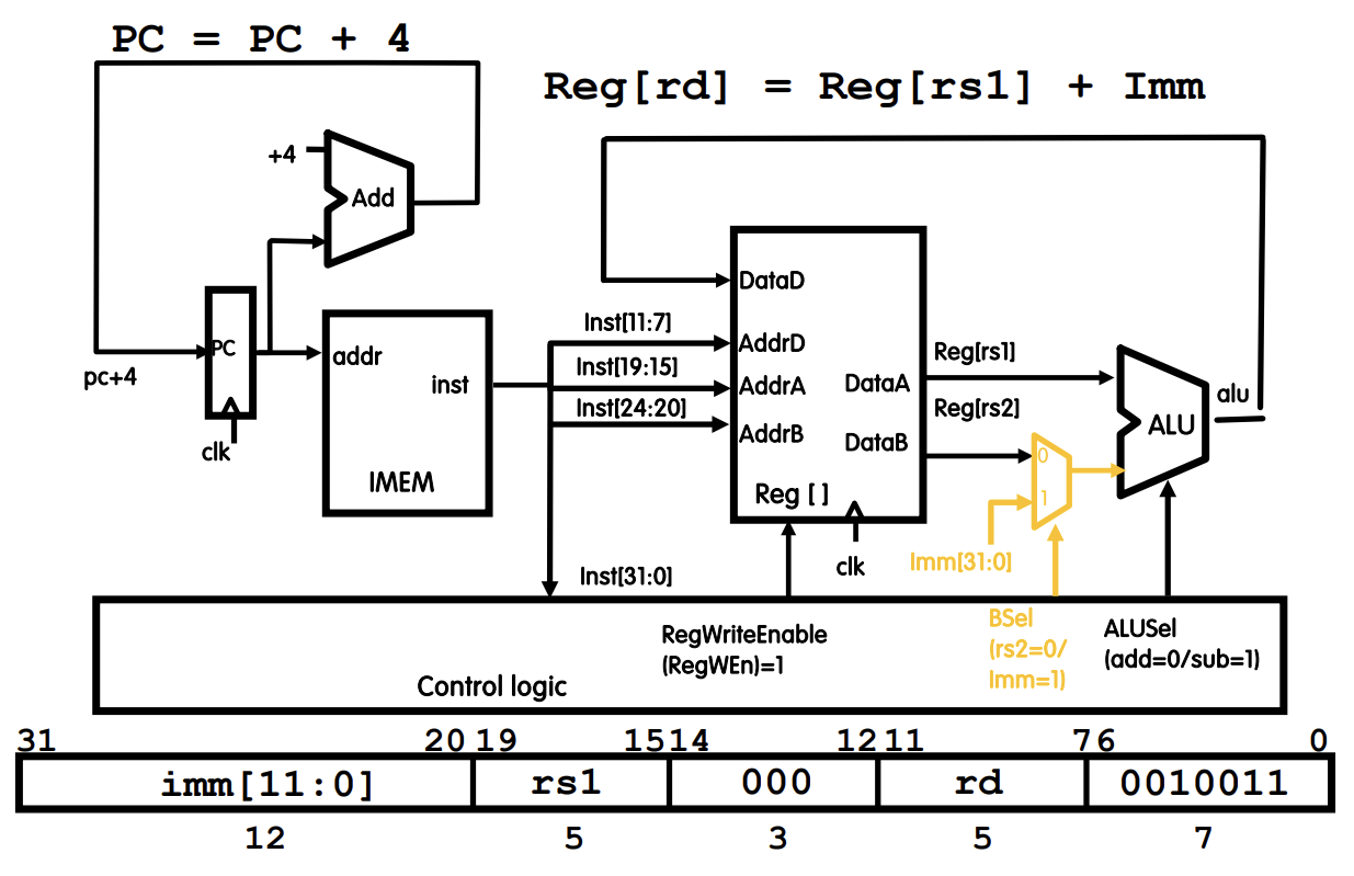 在 ALU 左侧加入一个多路复用器,根据 BSel 选择,如果 BSel = 0,则选择 rs2。如果 BSel = 1,则选择立即数。这两个输入都是 32 位值。 由于立即数在指令的上部只有 12 位宽,需要将他扩展为 32 位。需要添加一个小的模块进行对立即数的扩展。


 5884
5884

 被折叠的 条评论
为什么被折叠?
被折叠的 条评论
为什么被折叠?
 到【灌水乐园】发言


