


目录
1. 简介
PYNQ是一种基于Python的开发环境,专门设计用于快速、简便地在Xilinx的Zynq平台上进行开发。在《Zynq开发之-PYNQ配置,XVC(Xilinx Virtual Cable)调试_xilinx xvc-CSDN博客》博文中,我分享了使用 PYNQ 配置 XVC(Xilinx Virtual Cable) 调试 Zynq 代码,展示了PYNQ带来的巨大便利。它极大地简化了硬件加速器的设计流程,使得即使对于初学者来说,也能够快速上手。在之前的文章中,我们已经分享了如何使用PYNQ配置和进行XVC(Xilinx Virtual Cable)调试。
今天,我们将进一步探索PYNQ的应用领域,特别是在摄像头MIPI驱动方面。MIPI接口是一种高速串行接口标准,广泛用于连接图像传感器和图像处理器。本文将以OV5640摄像头为例,介绍如何利用PYNQ快速入门MIPI驱动开发。通过本文的学习,读者将能够掌握如何利用PYNQ快速搭建基于Zynq平台的图像处理系统,为后续的项目开发打下坚实的基础。
2. 配置代码
2.1 初始化寄存器
这段配置文件是用于配置相机或图像传感器的寄存器参数,以控制其工作模式、时钟频率、信号处理等方面的行为。
cfg = [
    [0x3008, 0x42], #[7]=0 Software reset; [6]=1 Software power down; Default=0x02

    [0x3103, 0x03], #[1]=1 System input clock from PLL; Default read = 0x11
    [0x3017, 0x00], #[3:0]=0000 MD2P,MD2N,MCP,MCN input; Default=0x00
    [0x3018, 0x00], #[7:2]=000000 MD1P,MD1N, D3:0 input; Default=0x00
    [0x3034, 0x18], #[6:4]=001 PLL charge pump, [3:0]=1000 MIPI 8-bit mode

#              +----------------+        +------------------+         +---------------------+        +---------------------+
#XVCLK         | PRE_DIV0       |        | Mult (4+252)     |         | Sys divider (0=16)  |        | MIPI divider (0=16) |
#+-------+-----> 3037[3:0]=0001 +--------> 3036[7:0]=0x38   +---------> 3035[7:4]=0001      +--------> 3035[3:0]=0001      |
#12MHz   |     | / 1            | 12MHz  | * 56             | 672MHz  | / 1                 | 672MHz | / 1                 |
#        |     +----------------+        +------------------+         +----------+----------+        +----------+----------+
#        |                                                                       |                              |
#        |                                                                       |                      MIPISCLK|672MHz
#        |                                                                       |                              |
#        |     +----------------+        +------------------+         +----------v----------+        +----------v----------+
#        |     | PRE_DIVSP      |        | R_DIV_SP         |         | PLL R divider       |        | MIPI PHY            | MIPI_CLK
#        +-----> 303d[5:4]=01   +--------> 303d[2]=0 (+1)   |         | 3037[4]=1 (+1)      |        |                     +------->
#              | / 1.5          |  8MHz  | / 1              |         | / 2                 |        | / 2                 | 336MHz
#              +----------------+        +---------+--------+         +----------+----------+        +---------------------+
#                                                  |                             |
#                                                  |                             |
#                                                  |                             |
#              +----------------+        +---------v--------+         +----------v----------+        +---------------------+
#              | SP divider     |        | Mult             |         | BIT div (MIPI 8/10) |        | SCLK divider        | SCLK
#              | 303c[3:0]=0x1  +<-------+ 303b[4:0]=0x19   |         | 3034[3:0]=0x8)      +----+---> 3108[1:0]=01 (2^)   +------->
#              | / 1            | 200MHz | * 25             |         | / 2                 |    |   | / 2                 | 84MHz
#              +--------+-------+        +------------------+         +----------+----------+    |   +---------------------+
#                       |                                                        |               |
#                       |                                                        |               |
#                       |                                                        |               |
#              +--------v-------+                                     +----------v----------+    |   +---------------------+
#              | R_SELD5 div    | ADCCLK                              | PCLK div            |    |   | SCLK2x divider      |
#              | 303d[1:0]=001  +------->                             | 3108[5:4]=00 (2^)   |    +---> 3108[3:2]=00 (2^)   +------->
#              | / 1            | 200MHz                              | / 1                 |        | / 1                 | 168MHz
#              +----------------+                                     +----------+----------+        +---------------------+
#                                                                                |
#                                                                                |
#                                                                                |
#                                                                     +----------v----------+        +---------------------+
#                                                                     | P divider (* #lanes)| PCLK   | Scale divider       |
#                                                                     | 3035[3:0]=0001      +--------> 3824[4:0]           |
#                                                                     | / 1                 | 168MHz | / 2                 |
#                                                                     +---------------------+        +---------------------+

    #PLL1 configuration
    [0x3035, 0x11], #[7:4]=0001 System clock divider /1, [3:0]=0001 Scale divider for MIPI /1
    [0x3036, 0x38], #[7:0]=56 PLL multiplier
    [0x3037, 0x11], #[4]=1 PLL root divider /2, [3:0]=1 PLL pre-divider /1
    [0x3108, 0x01], #[5:4]=00 PCLK root divider /1, [3:2]=00 SCLK2x root divider /1, [1:0]=01 SCLK root divider /2
    #PLL2 configuration
    [0x303D, 0x10], #[5:4]=01 PRE_DIV_SP /1.5, [2]=1 R_DIV_SP /1, [1:0]=00 DIV12_SP /1
    [0x303B, 0x19], #[4:0]=11001 PLL2 multiplier DIV_CNT5B = 25
    [0x3630, 0x36],
    [0x3631, 0x0e],
    [0x3632, 0xe2],
    [0x3633, 0x12],
    [0x3621, 0xe0],
    [0x3704, 0xa0],
    [0x3703, 0x5a],
    [0x3715, 0x78],
    [0x3717, 0x01],
    [0x370b, 0x60],
    [0x3705, 0x1a],
    [0x3905, 0x02],
    [0x3906, 0x10],
    [0x3901, 0x0a],
    [0x3731, 0x12],
    #VCM debug mode
    [0x3600, 0x08],
    [0x3601, 0x33],
    #System control register changing not recommended
    [0x302d, 0x60],
    #??
    [0x3620, 0x52],
    [0x371b, 0x20],
    #?? DVP
    [0x471c, 0x50],

    [0x3a13, 0x43],
    [0x3a18, 0x00],
    [0x3a19, 0xf8],
    [0x3635, 0x13],
    [0x3636, 0x03],
    [0x3634, 0x40],
    [0x3622, 0x01],
    [0x3c01, 0xa4],
    [0x3c04, 0x28],
    [0x3c05, 0x98],
    [0x3c06, 0x00],
    [0x3c07, 0x08],
    [0x3c08, 0x00],
    [0x3c09, 0x1c],
    [0x3c0a, 0x9c],
    [0x3c0b, 0x40],

    [0x503d, 0x00], #[7]=1 color bar enable, [3:2]=00 eight color bar
    [0x3820, 0x46], #[2]=1 ISP vflip, [1]=1 sensor vflip

    #[7:5]=010 Two lane mode, [4]=0 MIPI HS TX no power down, [3]=0 MIPI LP RX no power down,
    #[2]=1 MIPI enable, [1:0]=10 Debug mode; Default=0x58
    [0x300e, 0x45],
    #[5]=0 Clock free running, [4]=1 Send line short packet, [3]=0 Use lane1 as default,
    #[2]=1 MIPI bus LP11 when no packet; Default=0x04
    [0x4800, 0x14],
    [0x302e, 0x08],
    #[7:4]=0x3 YUV422, [3:0]=0x0 YUYV
    #(0x4300, 0x30),
    #[7:4]=0x6 RGB565, [3:0]=0x0 (b[4:0],g[5:3],g[2:0],r[4:0])
    [0x4300, 0x6f],
    [0x501f, 0x01],

    [0x4713, 0x03],
    [0x4407, 0x04],
    [0x440e, 0x00],
    [0x460b, 0x35],
    [0x460c, 0x20], #[1]=0 DVP PCLK divider manual control by 0x3824[4:0]
    [0x3824, 0x01], #[4:0]=1 SCALE_DIV=INT(3824[4:0]/2)

    #MIPI timing
    #  [0x4805, 0x10], #LPX global timing select=auto
    #  [0x4818, 0x00], #hs_prepare + hs_zero_min ns
    #  [0x4819, 0x96],
    #  [0x482A, 0x00], #hs_prepare + hs_zero_min UI
    #
    #  [0x4824, 0x00], #lpx_p_min ns
    #  [0x4825, 0x32],
    #  [0x4830, 0x00], #lpx_p_min UI
    #
    #  [0x4826, 0x00], #hs_prepare_min ns
    #  [0x4827, 0x32],
    #  [0x4831, 0x00], #hs_prepare_min UI

    #[7]=1 LENC correction enabled, [5]=1 RAW gamma enabled, [2]=1 Black pixel cancellation enabled,
    #[1]=1 White pixel cancellation enabled, [0]=1 Color interpolation enabled
    [0x5000, 0x07],
    #[7]=0 Special digital effects, [5]=0 scaling, [2]=0 UV average disabled,
    #[1]=1 Color matrix enabled, [0]=1 Auto white balance enabled
    [0x5001, 0x03]
]
2.2 分辨率寄存器
以下代码实现 720p @ 60fps:
res_720p = [
#1280 x 720 binned, RAW10, MIPISCLK=280M, SCLK=56Mz, PCLK=56M
    [0x3008, 0x42], #PLL1 configuration
    [0x3035, 0x21], #[7:4]=0010 System clock divider /2, [3:0]=0001 Scale divider for MIPI /1
    [0x3036, 90], #[7:0]=70 PLL multiplier
    [0x3037, 0x02], #[4]=0 PLL root divider /1, [3:0]=2 PLL pre-divider /2
    [0x3108, 0x11], #[5:4]=01 PCLK root divider /2, [3:2]=00 SCLK2x root divider /1, [1:0]=01 SCLK root divider /2

    [0x3034, 0x1A], #[6:4]=001 PLL charge pump, [3:0]=1010 MIPI 10-bit mode
    [0x3800, (0 >> 8) & 0x0F], #[3:0]=0 X address start high byte
    [0x3801,  0       & 0xFF], #[7:0]=0 X address start low byte
    [0x3802, (8 >> 8) & 0x07], #[2:0]=0 Y address start high byte
    [0x3803,  8       & 0xFF], #[7:0]=0 Y address start low byte

    [0x3804, (2619 >> 8) & 0x0F], #[3:0] X address end high byte
    [0x3805,  2619       & 0xFF], #[7:0] X address end low byte
    [0x3806, (1947 >> 8) & 0x07], #[2:0] Y address end high byte
    [0x3807,  1947       & 0xFF], #[7:0] Y address end low byte

    [0x3810, (0 >> 8) & 0x0F], #[3:0]=0 timing hoffset high byte
    [0x3811,  0       & 0xFF], #[7:0]=0 timing hoffset low byte
    [0x3812, (0 >> 8) & 0x07], #[2:0]=0 timing voffset high byte
    [0x3813,  0       & 0xFF], #[7:0]=0 timing voffset low byte

    [0x3808, (1280 >> 8) & 0x0F], #[3:0] Output horizontal width high byte
    [0x3809,  1280       & 0xFF], #[7:0] Output horizontal width low byte
    [0x380a, (720  >> 8) & 0x7F], #[2:0] Output vertical height high byte
    [0x380b,  720        & 0xFF], #[7:0] Output vertical height low byte

    [0x380c, (1896 >> 8) & 0x1F], #HTS line exposure time in # of pixels
    [0x380d,  1896       & 0xFF],
    [0x380e, (984  >> 8) & 0xFF], #VTS frame exposure time in # lines
    [0x380f,  984        & 0xFF],

    [0x3814, 0x31], #[7:4]=0x3 horizontal odd subsample increment, [3:0]=0x1 horizontal even subsample increment
    [0x3815, 0x31], #[7:4]=0x3 vertical odd subsample increment, [3:0]=0x1 vertical even subsample increment
    [0x3821, 0x01], #[2]=0 ISP mirror, [1]=0 sensor mirror, [0]=1 horizontal binning
    [0x4837, 36], # 1/56M*2 #little MIPI shit: global timing unit, period of PCLK in ns * 2(depends on # of lanes)

    #Undocumented anti-green settings
    [0x3618, 0x00], # Removes vertical lines appearing under bright light
    [0x3612, 0x59],
    [0x3708, 0x64],
    [0x3709, 0x52],
    [0x370c, 0x03],

    [0x4300, 0x00], #[7:4]=0x0 Formatter RAW, [3:0]=0x0 BGBG/GRGR
    [0x501f, 0x03], #[2:0]=0x3 Format select ISP RAW (DPC)
    [0x3008, 0x02],
]
2.3 白平衡寄存器
awb = [
    # Disable Advanced AWB
    [0x518d ,0x00],
    [0x518f ,0x20],
    [0x518e ,0x00],
    [0x5190 ,0x20],
    [0x518b ,0x00],
    [0x518c ,0x00],
    [0x5187 ,0x10],
    [0x5188 ,0x10],
    [0x5189 ,0x40],
    [0x518a ,0x40],
    [0x5186 ,0x10],
    [0x5181 ,0x58],
    [0x5184 ,0x25],
    [0x5182 ,0x11],

    # Enable simple AWB
    [0x3406 ,0x00],
    [0x5183 ,0x80],
    [0x5191 ,0xff],
    [0x5192 ,0x00],
    [0x5001 ,0x03]
]
2.4 配置寄存器代码
这段代码的作用是通过迭代三个不同的列表cfg、awb和res_720p,分别发送配置命令到摄像头模块,实现初始化摄像头模块,并配置其工作模式、白平衡(AWB)以及视频分辨率(720p)。
for cmd in cfg:
    first = cmd[0].to_bytes(2,'big')
    #print(hex(first[0]), hex(first[1]), hex(cmd[1]))
    write_cam_dat([first[0],first[1],cmd[1]])
print("Init complete")

for cmd in awb:
    first = cmd[0].to_bytes(2,'big')
    #print(hex(first[0]), hex(first[1]), hex(cmd[1]))
    write_cam_dat([first[0],first[1],cmd[1]])
print("AWB complete")

for cmd in res_720p:
    first = cmd[0].to_bytes(2,'big')
    #print(hex(first[0]), hex(first[1]), hex(cmd[1]))
    write_cam_dat([first[0],first[1],cmd[1]])
print("Video mode complete")
2.5 顶层代码
from pynq import Overlay, GPIO, allocate
from pynq.lib import AxiIIC
from pynq.lib.video import *
import PIL.Image
import cv2
import matplotlib.pyplot as plt
import scipy.ndimage
import matplotlib.image as mpimg
from pynq.lib.debugbridge import DebugBridge
from time import sleep
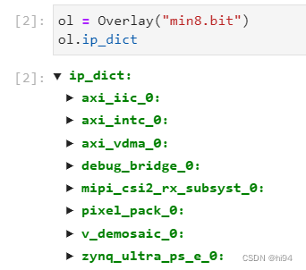
ol = Overlay("min8.bit")
ol.ip_dict
db = DebugBridge(ol.ip_dict['debug_bridge_0'])
db.start_xvc_server(bufferLen=4096, serverAddress="192.168.101.224", serverPort=2542, reconnect=True, verbose=True)
axi_iic = AxiIIC(ol.ip_dict["axi_iic_0"])
cam_en = GPIO(GPIO.get_gpio_pin(0), 'out')
cam_en.write(1)
axi_iic.send(0x74, [0x04], 1, 0)
ctrl_reg = bytes(1)
axi_iic.receive(0x74, ctrl_reg, 1, 0)
for address in range(0x00, 0x8f):
try:
# Attempt to read 1 byte from the current address
axi_iic.receive(address, [0x00], 1, 0)
print(f"Found I2C device at address: 0x{address:02X}")
except Exception:
# No response from the current address
pass
def read_cam_dat(cam_reg, n):
axi_iic.send(0x3c, cam_reg, len(cam_reg), 0)
rx_data = bytes(n)
axi_iic.receive(0x3c, rx_data, n, 0)
axi_iic.wait()
print(' '.join(f'{byte:02x}' for byte in rx_data))
def write_cam_dat(cam_regs):
axi_iic.send(0x3c, cam_regs, len(cam_regs), 0)
rx_data = bytes(1)
axi_iic.send(0x3c, [cam_regs[0], cam_regs[1]], len(cam_regs)-1, 0)
axi_iic.receive(0x3c, rx_data, 1, 0)
#print(' '.join(f'readback: {byte:02x}' for byte in rx_data))
#sleep(0.05)
WIDTH = 1280
HEIGHT = 720
demo = ol.v_demosaic_0
demo.write(0x10,WIDTH)
demo.write(0x18,HEIGHT)
demo.write(0x28,0x03)
demo.write(0x00,0x81)
pixel_in = ol.pixel_pack_0
pixel_in.bits_per_pixel = 24
vdma = ol.axi_vdma_0
cam_vdma = ol.axi_vdma_0
cam_vdma.readchannel.mode = VideoMode(WIDTH, HEIGHT, 24)
cam_vdma.readchannel.start()
%run pcam_cfg.ipynb
frame_camera = cam_vdma.readchannel.readframe()
frame_color=cv2.cvtColor(frame_camera,cv2.COLOR_BGR2RGB)
pixels = np.array(frame_color)
plt.imshow(pixels)
plt.show()
3. 细节指引
以上信息需要建立在读者了解 PYNQ 的基本用法,并熟悉 iPython 的基本操作。
以下信息仅提供关键步骤的指引,如需更加具体的操作,请私信。
- 通过 ip_dict 查看 PYNQ Overlay 所报告的 IP
- 通过 DebugBridge IP Core 可以快速分析 mipi 端口接收到的数据。

- 通过 write_cam_dat([0x30, 0x08, 0x82]) 指令可以快速开启/关闭摄像头,观察初始数据。
- 以下调试代码可以快速查看摄像头状态:
# 通过读取寄存器确保 MIPI DPHY 和 MIPI CSI-2 RX 控制器内核处于启用状态。
#ol.mipi_csi2_rx_subsyst_0.register_map.core_configuration
# 通过读取寄存器确保 MIPI DPHY 和 MIPI CSI-2 RX 控制器内核处于启用状态。
#ol.mipi_csi2_rx_subsyst_0.register_map.dphy_control
# Clock Lane 和 Data Line 状态信息
#ol.mipi_csi2_rx_subsyst_0.register_map.dphy_cl_status
#ol.mipi_csi2_rx_subsyst_0.register_map.dphy_dl0_status
4. 总结
本文深入探讨了基于PYNQ的Zynq平台上摄像头MIPI驱动的快速入门方法。首先,我们通过介绍PYNQ开发环境及其在Zynq平台上的便利性,为读者提供了必要的背景知识。接着,以OV5640摄像头为例,详细介绍了配置摄像头寄存器、设置分辨率和白平衡参数等关键步骤,并通过Python代码展示了如何利用PYNQ库与摄像头模块进行通信和配置。最后,我们给出了一些细节指引和调试方法,帮助读者更好地理解和应用所学知识。


 952
952

 被折叠的 条评论
为什么被折叠?
被折叠的 条评论
为什么被折叠?
 到【灌水乐园】发言


