


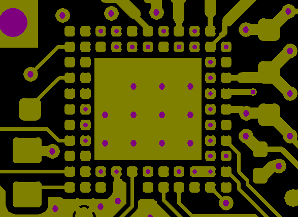
n PCB design, via is a common connection that connects different layers of wiring or provides a place for components to be soldered. There are various types of via, one of which is via in pad (via in pad), that is, the via is punched on the SMD or BGA pad, and then the hole is plugged with resin and plated with a layer of copper on the surface, so that the hole is not visible on the pad.
Advantages and Disadvantages of Vid in Pad
Vid in Pad (Vid in Pad) is the basic structure of HDI (High Density Interconnect) boards, and its advantages are obvious: reduce the distance between boards and signal transmission distance, which is beneficial to reduce signal interference and loss; plating filled with copper solid holes can effectively reduce the parasitic signals in the holes and parasitic inductance, which is conducive to the transmission of high-frequency signals; effectively reduce the thickness of the finished board, and increase the density of the wiring per unit area, and so on.
But the hole in the disk also has some disadvantages, such as high cost, long production cycle, easy to produce bubbles and so on. One of the most serious problems is the void, i.e., the bubble or gap formed inside the solder joint. Voids can affect the mechanical strength and thermal conductivity of the solder joint, leading to poor or failed soldering. Therefore, care needs to be taken to avoid or minimize the creation of voids when designing and manufacturing hole-in-disks.
Translated with DeepL.com (free version)
Causes of cavities:
1. Inadequate or uneven resin plugging. Resin plugging is one of the key processes for hole-in-disk, which requires the over-hole to be completely filled and cured to prevent solder paste from flowing into the over-hole. Inadequate or uneven resin plugging can result in trapped air inside the hole or gaps caused by shrinkage of the resin. These spaces can be filled with solder paste during soldering and form voids.
2. The plating cap is not flat or firm. Plating cap is in the resin after plugging holes in the pad surface plated with a layer of copper to increase the soldering area and wettability. If the plating cap is not flat or not firm, will lead to solder paste and copper layer between the gap or separation phenomenon, these gaps or separation will also form a hole.
3. The solder paste itself contains oxygen or other impurities. Solder paste is used to connect components and PCB metal materials, it usually contains a certain proportion of flux and other additives. These fluxes and additives at high temperatures will have a chemical reaction or volatilization, resulting in oxygen or other gases.
4. Inappropriate soldering temperature. Soldering temperature is an important factor affecting the fluidity and wettability of solder paste. If the temperature is too high or the heating time is too long, it will lead to excessive oxidation or volatilization of the solder paste, generating a large amount of gas; if the temperature is too low or the heating time is too short, it will lead to poor fluidity of the solder paste or solidify too quickly, hindering the gas discharge.
How to avoid the problem of hollow holes in the disk
1. Optimize the resin hole plugging process. Resin hole plugging process needs to control the type of resin, viscosity, temperature, pressure, time and other parameters to ensure that the resin can fully and uniformly fill the holes, and do not produce shrinkage or cracking after curing.
2. Optimize the plating cap process. Plating cap process needs to control the composition of the plating solution, temperature, concentration, current, time and other parameters to ensure that the plating layer can be flat and firmly covered in the pads, and with the resin and the substrate has good adhesion. At the same time, it is necessary to choose a suitable copper reduction method to remove excess copper and keep the surface flat.
3. Select and use the appropriate solder paste. The selection and use of solder paste need to consider its compatibility with the components and PCB, wettability, oxidization, volatility and other characteristics, in order to reduce the generation of gas and residue.
4. Optimize the soldering temperature and time. Soldering to choose the appropriate reflow temperature and time to ensure that the solder paste is fully wetted and flowing.
Fitech Solder Paste
Fuyingda Shenzhen is able to produce high quality, high performance and high reliability solder pastes for a variety of PCB design and manufacturing processes, including hole-in-disk and microvia.


 810
810

 被折叠的 条评论
为什么被折叠?
被折叠的 条评论
为什么被折叠?
 到【灌水乐园】发言


