


配置一个简单的pwm,上次我们已经完成了,这次主要来说说中断的配置流程。
如何配置pwm参考
https://blog.csdn.net/a3431509393/article/details/139014404?spm=1001.2014.3001.5501
想要配置spwm 就要清楚基波和载波的频率关系,我们配置基波为20k载波为20hz的spwm,先配置时钟为20k
#ifdef _LAUNCHXL_F28377S
    InitSysPll(XTAL_OSC,IMULT_40,FMULT_0,PLLCLK_BY_2);
#else
    InitSysPll(XTAL_OSC,IMULT_20,FMULT_0,PLLCLK_BY_2);
#endif
系统频率
    EPwm2Regs.TBPRD = 2500;                       // Set timer period
    EPwm2Regs.TBPHS.bit.TBPHS = 0x0000;           // Phase is 0
    EPwm2Regs.TBCTR = 0x0000;                     // Clear counter


    //
    // Setup TBCLK
    //
    EPwm2Regs.TBCTL.bit.CTRMODE = TB_COUNT_UPDOWN; // Count up
    EPwm2Regs.TBCTL.bit.PHSEN = TB_DISABLE;        // Disable phase loading
    EPwm2Regs.TBCTL.bit.HSPCLKDIV = TB_DIV1;       // Clock ratio to SYSCLKOUT
    EPwm2Regs.TBCTL.bit.CLKDIV = TB_DIV1;          // Slow just to observe on
                                                   // the scope
时钟频率
这样便是20khz的基波
下来我们的思路,在每一次计数器到0时,进中断,每进一次中断计数器加一,五十次后,在中断中改变比较值并清除中断计数器。
中断配置流程如下:
1 . 全局禁用中断
//
// Step 3. Clear all interrupts and initialize PIE vector table:
// Disable CPU interrupts
//
    DINT;
2 . 通过ENPIE位使能PIE.
//
// EnableInterrupts - This function enables the PIE module and CPU __interrupts
//
void EnableInterrupts()
{
    //
    // Enable the PIE
    //
    PieCtrlRegs.PIECTRL.bit.ENPIE = 1;

	//
    // Enables PIE to drive a pulse into the CPU
    //
	PieCtrlRegs.PIEACK.all = 0xFFFF;

	//
    // Enable Interrupts at the CPU level
    //
    EINT;
}
3 . 将中断向量写入中断向量表
//
// InitPieVectTable - This function initializes the PIE vector table to a known
// state. This function must be executed after boot time.
//
void
InitPieVectTable(void)
{
    int16 i;
    Uint32 *Source = (void *) &PieVectTableInit;
    Uint32 *Dest = (void *) &PieVectTable;

    //
    // Do not write over first 3 32-bit locations (these locations are
    // initialized by Boot ROM with boot variables)
    //
    Source = Source + 3;
    Dest = Dest + 3;

    EALLOW;
    for(i=0; i < 221; i++)
    {
        *Dest++ = *Source++;
    }
    EDIS;
}
4 . 第四步可以暂时不考虑,咱们用的是定时器中断
5 . 为所需的中断配置CPU_IER位
//
// Enable CPU INT3 which is connected to EPWM1-3 INT:
//
    IER |= M_INT3;
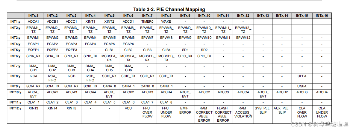
注明:这里的M_INT3是查表得到的,可以查:
6 . 在外设中使能中断
    //
    // Interrupt where we will modify the deadband
    //
    EPwm2Regs.ETSEL.bit.INTSEL = ET_CTR_ZERO;     // Select INT on Zero event
    EPwm2Regs.ETSEL.bit.INTEN = 1;                // Enable INT
    EPwm2Regs.ETPS.bit.INTPRD = ET_1ST;           // Generate INT on 3rd event
7 . 全局启用中断
//
// Enable global Interrupts
//
    EINT;  // Enable Global interrupt INTM
这样终端就配置完成了;
下来是终端里的内容每50次改变一次比较值,对应的spwm需要400个点。
//
// epwm2_isr - EPWM2 ISR
//
__interrupt void epwm2_isr(void)
{
    if(EPwm2TimerIntCount == 50)
    {
        EPwm2TimerIntCount = 0;
        EPwm2Regs.CMPA.bit.CMPA = ESpwm[i];
        i++;
        if(i == 400)
        {
            i = 0;
        }
    }

    EPwm2TimerIntCount++;

    //
    // Clear INT flag for this timer
    //
    EPwm2Regs.ETCLR.bit.INT = 1;

    //
    // Acknowledge this interrupt to receive more interrupts from group 3
    //
    PieCtrlRegs.PIEACK.all = PIEACK_GROUP3;
}
这样就可以了,spwm表如下:
 Uint16 ESpwm[] = {
                   1250,1268,1287,1306,1325,1344,1362,1381,1400,1419,1437,1456,1474,1493,1511,1530,
                   1548,1566,1584,1602,1620,1638,1656,1674,1691,1709,1726,1743,1760,1777,1794,1811,
                   1828,1844,1860,1876,1892,1908,1924,1940,1955,1970,1985,2000,2014,2029,2043,2057,
                   2071,2085,2098,2111,2124,2137,2150,2162,2174,2186,2198,2209,2220,2231,2242,2252,
                   2263,2273,2282,2292,2301,2310,2319,2327,2335,2343,2351,2358,2365,2372,2379,2385,
                   2391,2396,2402,2407,2412,2416,2421,2425,2428,2432,2435,2438,2440,2442,2444,2446,
                   2447,2448,2449,2449,2450,2449,2449,2448,2447,2446,2444,2442,2440,2438,2435,2432,
                   2428,2425,2421,2416,2412,2407,2402,2396,2391,2385,2379,2372,2365,2358,2351,2343,
                   2335,2327,2319,2310,2301,2292,2282,2273,2263,2252,2242,2231,2220,2209,2198,2186,
                   2174,2162,2150,2137,2124,2111,2098,2085,2071,2057,2043,2029,2014,2000,1985,1970,
                   1955,1940,1924,1908,1892,1876,1860,1844,1828,1811,1794,1777,1760,1743,1726,1709,
                   1691,1674,1656,1638,1620,1602,1584,1566,1548,1530,1511,1493,1474,1456,1437,1419,
                   1400,1381,1362,1344,1325,1306,1287,1268,1250,1231,1212,1193,1174,1155,1137,1118,
                   1099,1080,1062,1043,1025,1006,988,969,951,933,915,897,879,861,843,825,
                   808,790,773,756,739,722,705,688,671,655,639,623,607,591,575,559,
                   544,529,514,499,485,470,456,442,428,414,401,388,375,362,349,337,
                   325,313,301,290,279,268,257,247,236,226,217,207,198,189,180,172,
                   164,156,148,141,134,127,120,114,108,103,97,92,87,83,78,74,
                   71,67,64,61,59,57,55,53,52,51,50,50,50,50,50,51,
                   52,53,55,57,59,61,64,67,71,74,78,83,87,92,97,103,
                   108,114,120,127,134,141,148,156,164,172,180,189,198,207,217,226,
                   236,247,257,268,279,290,301,313,325,337,349,362,375,388,401,414,
                   428,442,456,470,485,499,514,529,544,559,575,591,607,623,639,655,
                   671,688,705,722,739,756,773,790,808,825,843,861,879,897,915,933,
                   951,969,988,1006,1025,1043,1062,1080,1099,1118,1137,1155,1174,1193,1212,1231

 };
这个表可以通过直接算,或者辅助工具生成。
这样spwm就配置完成。配上主函数的内容:
//
// Main
//
void main(void)
{
//
// Step 1. Initialize System Control:
// PLL, WatchDog, enable Peripheral Clocks
// This example function is found in the F2837xS_SysCtrl.c file.
//
    InitSysCtrl();

//
// Step 2. Initialize GPIO:
// This example function is found in the F2837xS_Gpio.c file and
// illustrates how to set the GPIO to its default state.
//
//    InitGpio();

//
// enable PWM1, PWM2 and PWM3
//

    CpuSysRegs.PCLKCR2.bit.EPWM2=1;


//
// For this case just init GPIO pins for ePWM1, ePWM2, ePWM3
// These functions are in the F2837xS_EPwm.c file
//
//    InitEPwm1Gpio();
    InitEPwm2Gpio();
//    InitEPwm3Gpio();

//
// Step 3. Clear all interrupts and initialize PIE vector table:
// Disable CPU interrupts
//
    DINT;

//
// Initialize the PIE control registers to their default state.
// The default state is all PIE interrupts disabled and flags
// are cleared.
// This function is found in the F2837xS_PieCtrl.c file.
//
    InitPieCtrl();
    EnableInterrupts();
//
// Disable CPU interrupts and clear all CPU interrupt flags:
//
    IER = 0x0000;
    IFR = 0x0000;

//
// Initialize the PIE vector table with pointers to the shell Interrupt
// Service Routines (ISR).
// This will populate the entire table, even if the interrupt
// is not used in this example.  This is useful for debug purposes.
// The shell ISR routines are found in F2837xS_DefaultIsr.c.
// This function is found in F2837xS_PieVect.c.
//
    InitPieVectTable();

//
// Interrupts that are used in this example are re-mapped to
// ISR functions found within this file.
//
    EALLOW; // This is needed to write to EALLOW protected registers
//    PieVectTable.EPWM1_INT = &epwm1_isr;
    PieVectTable.EPWM2_INT = &epwm2_isr;
//    PieVectTable.EPWM3_INT = &epwm3_isr;
    EDIS;   // This is needed to disable write to EALLOW protected registers

//
// Step 4. Initialize the Device Peripherals:
//
    EALLOW;
    CpuSysRegs.PCLKCR0.bit.TBCLKSYNC =0;
    EDIS;

//    InitEPwm1Example();
    InitEPwm2Example();
//    InitEPwm3Example();

    EALLOW;
    CpuSysRegs.PCLKCR0.bit.TBCLKSYNC =1;
    EDIS;

//
// Step 5. User specific code, enable interrupts:
// Initialize counters:
//

//
// Enable CPU INT3 which is connected to EPWM1-3 INT:
//
    IER |= M_INT3;

//
// Enable EPWM INTn in the PIE: Group 3 interrupt 1-3
//
//    PieCtrlRegs.PIEIER3.bit.INTx1 = 1;
    PieCtrlRegs.PIEIER3.bit.INTx2 = 1;
//    PieCtrlRegs.PIEIER3.bit.INTx3 = 1;

//
// Enable global Interrupts and higher priority real-time debug events:
//
    EINT;  // Enable Global interrupt INTM
    ERTM;  // Enable Global realtime interrupt DBGM

//
// Step 6. IDLE loop. Just sit and loop forever (optional):
//
    for(;;)
    {
        asm ("          NOP");
    }
}
有一点需要注明一下,实际测试中,死区极性是反的这里要配置为
    //
    // Active Low complementary PWMs - setup the deadband
    //
    EPwm2Regs.DBCTL.bit.OUT_MODE = DB_FULL_ENABLE;
    EPwm2Regs.DBCTL.bit.POLSEL = DB_ACTV_HIC;
    EPwm2Regs.DBCTL.bit.IN_MODE = DBA_ALL;
    EPwm2Regs.DBRED.bit.DBRED = EPWM2_MAX_DB;
    EPwm2Regs.DBFED.bit.DBFED = EPWM2_MAX_DB;
//HIC为正常死区,若为LOC则会导致高电平还没掉下来,
//低电平就上去了,死区时间越长,上下开关管同时导通时间越长


 1248
1248


 被折叠的 条评论
为什么被折叠?
被折叠的 条评论
为什么被折叠?
 到【灌水乐园】发言


