


Chapter 1
Introduction
1.1 Fundamentals of Hardware Security
In our modern age of omnipresent and highly interconnected information technology,
cybersecurity becomes ever more challenged. For example, with the rise of
the Internet of Things (IoT), most such equipment is connected to the internet in
some way, often inscrutable to the regular customers. This fact opens up large
attack surfaces and can lead to severe ramifications (Fig. 1.1), as demonstrated
through a plethora of real-world attacks over many years. Within the realm of
cybersecurity, hardware security in particular is concerned about achieving security
and trust directly within the underlying electronics. For example, researchers have
cautioned against powerful attacks on the speculative execution of modern processors
[Koc+19a, Lip+18a] or profiled the side-channel leakage of cryptographic
hardware modules [Ler+18]. For another example, the so-called root of trust
(RoT) techniques for isolation and attestation of computation are found in many
commercial computers and other custom devices [Mae+18, Zha+19, Nab+20].
第一章 简介
1.1硬件安全基础
在当今这个信息技术无所不在且高度互联的时代,网络安全正变得越来越具有挑战性。例如,随着物联网 (IoT) 的兴起,大多数此类设备都会通过某种方式接入互联网,通常普通用户也难以理解其背后的机理。正如图 1.1中所描述的历年来发生在现实世界中的海量攻击所示,这事实上扩大了攻击面,并会导致严重的后果。在网络安全的领域中,硬件安全着重关注直接通过底层的电子器件来实现安全和信任。例如,研究人员曾提醒人们注意针对现代处理器的推测性执行的严重攻击[Koc+19a, Lip+18a],抑或剖析了加密硬件模块的侧信道泄漏问题[Ler+18]。再比如,在许多商用计算机和其他定制设备中,都使用了所谓的信任根(RoT)技术,用于计算的隔离和证明[Mae+18, Zha+19, Nab+20]。
Next, we discuss the fundamental aspects of hardware security and review
selected prior art, which will be assumed as common knowledge throughout the
remaining chapters of this monograph. It should be understood that this chapter can
provide only an overview on this vast and fast-growing field, but we review the most
important aspects and seminal protection schemes here to equip the reader with the
necessary background to follow this monograph.
接下来,我们将讨论硬件安全的基本方面并对所选现有技术进行回顾,在本专著的其余章节中,这些内容将被认定为常识。
应该理解的是,本章仅能对此广阔且飞速发展的领域提供一个概述,但我们会聚焦于其中重要的技术方面和最具开创性的保护方案,使得读者可掌握必要的背景知识,以理解本专著。
1.1.1 Data Security at Runtime
The confidentiality, integrity, and availability of data processing within electronics
are subject to various threat scenarios, like (1) unauthorized access or modification

Fig. 1.1 Modern devices are deployed all around us and often connected to the internet but
typically lack built-in notions and measures for security. Thus, a plethora of risks arise for everyday
life. Adopted from [Gra16]
of data and (2) attacks leveraging side-channels, fault-injection, physical read-out
or probing.
1.1.1 运行时数据安全
电子产品中数据处理的保密性、完整性和可用性会受到各种威胁的影响,诸如(1)对数据的未经授权的访问或修改,(2)利用
侧信道、故障注入、物理读取或探测的攻击。
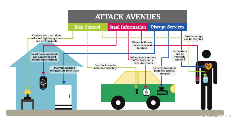
图1.1 现代的硬件设备部署在我们周边,且与互联网连接,但通常缺乏内置的安全概念和措施。因此,在给人们的日常生活
带来了大量的安全风险。本图摘自[Gra16]。
1.1.1.1 Unauthorized Access or Modification of Data
Conventional attacks seeking to steal or corrupt data are conducted mainly at the
software level and for interconnected systems. Cryptography represents a commonly
applied protection scheme here, but there are also many dedicated, hardware-centric
security features. For example, there are:
• Enclaves for trusted execution (TEEs), like the industrial ARM TrustZone and
Intel SGX or the academic MIT Sanctum (Fig. 1.2; see also [Mae+18] for more
background on each TEE)
• Wrappers for monitoring and cross-checking of untrusted third-party intellectual
property (IP) modules [Bas+17]
• Centralized IP infrastructures for secure system design [Wan+15b]
• Verification of computation [Wah+16]
• Secure task scheduling [Liu+14]
• Secure network-on-chip (NoC) architectures [Fio+08], etc.
However, if not designed and implemented carefully, such security features
become prone to hardware-centric attacks themselves, e.g., see [BCO04, Bay+16,
Qiu+19, OD19, CH17]; such attacks are discussed in more detail throughout this
section.
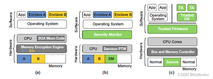
Fig. 1.2 Enclaves for trusted execution are prominent hardware-centric security features. Illustrated
are the high-level architectures of (a) Intel SGX, (b) MIT Sanctum, and © ARM TrustZone
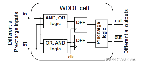
Fig. 1.3 Wave dynamic differential logic (
WDDL) serves to mitigate power side-channel attacks.
This is achieved by redundant, differential combinational logic paths that switch in opposite
directions for any operation, thereby obfuscating differences in power consumption for particular
transitions. Furthermore, pre-charge logic is used to reduce peak power consumption during
switching. Adopted from [Fuj+14]
1.1.1.1 对数据未经授权的访问或修改
试图窃取或破坏数据的常规攻击主要在软件层面和互连系统上实施。对此,密码学代表了一种普遍适用的保护方案,但如下所示,也有许多专用的、以硬件为中心的安全保护特性:
• 用于可信执行的隔离飞地 (TEEs), 诸如工业界中的ARM TrustZone、Intel SGX,学术界的MIT Sanctum解决方案 (参见Fig. 1.2; 关于每种TEE的更多背景,请参见[Mae+18])
• 用于监视和交叉检查不受信任的第三方知识产权(IP)模块的包装器[Bas+17]
• 用于系统设计安全的集中式知识产权保护(IP)基础设施 [Wan+15b]
• 计算验证 [Wah+16]
• 安全的任务调度 [Liu+14]
• 安全的片上网络 (NoC) 架构 [Fio+08]等。
然而,如果缺乏精心的设计和实现,上述安全特性本身也容易遭受针对硬件的攻击。具体而言,可参考 章节[BCO04, Bay+16,
Qiu+19, OD19, CH17],其中对此类攻击进行了更加详细的讨论。

Fig. 1.2 用于可信执行的隔离飞地是典型的以硬件为中心的安全特性。图中所示分别为 (a)Intel SGX,(b)MIT Sanctum和©ARM TrustZone的高级架构。

Fig. 1.3 波动差分逻辑( WDDL)可用于缓解功耗侧信道攻击。这是通过冗余的差分组合逻辑路径实现的,这些路径针对任何操作都实施反向切换,从而掩盖了特定状态转移的功耗差异。此外,预充电逻辑也被用来降低切换期间的峰值功耗。本图摘自[Fuj+14]。
1.1.1.2 Side-Channel and Fault-Injection Attacks
Side-channel attacks infer information from physical channels that are leaky due to
the sensitivity and vulnerability of the underlying electronics [ZF05]. For example,
it is well-known that the Advanced Encryption Standard (AES) is vulnerable
to power side-channel attacks when the hardware implementation is unprotected
[BCO04, OD19, SW12]. Another instance is the leakage of information related to
timing behavior or speculative execution in modern processors, through caches and
other buffers [OST05, Lip+18a, Sch+19].
1.1.1.2 侧信道与故障注入攻击
由于底层电子器件的敏感性和脆弱性,侧信道攻击可利用物理信道的泄露推断出相关信息[ZF05]。例如,
众所周知,当硬件实现未采取保护措施时,高级加密标准 (AES) 易遭受基于功耗的侧信道攻击[BCO04, OD19, SW12]。
另外一个例子事关信息的泄露,与现代处理器中的定时行为,或者基于高速缓存与缓冲区的推测执行特性有关 [OST05, Lip+18a, Sch+19]。
Most countermeasures against side-channel attacks apply some kind of cloaking
or masking technique, which involves the diffusion of the information leaked
through side-channels. This is achieved by various means, ranging from systemlevel
solutions [GMK16], down to individual gates [Bel+18]. See also Fig. 1.3 for
an example. Nevertheless, the resilience of such countermeasures is still subject to
the physical implementation in its entirety. For example, Fujimoto et al. [Fuj+14].
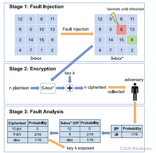
Fig. 1.4 Multi-stage attack on AES. First, a random but persistent fault is injected into the S-box,
to bias the subsequent encryption. In turn, the bias helps to infer the secret key while sampling over
a sufficiently large number of cipher-texts. Adopted from [Pan+19]
have shown that even the promising WDDL scheme suffers from minute layoutlevel
asymmetries, allowing an attacker to eventually infer the secret key.
大多数针对侧信道攻击的安全对策都采用了某种隐身或屏蔽技术。这涉及到对于通过侧信道泄露的信息扩散的控制。
具体可通过各种手段实现,包括从整系统级[GMK16]到单个门电路[Bel+18]的解决方案,另见图1.3的例子。然而,此类对策的韧性仍取决于其整体上的物理实现。例如,Fujimoto等人[Fuj+14]已证明,即使先进的WDDL方案也会遭受布局上的微弱不对称的影响,使得攻击者最终可推导出密钥。

Fig. 1.4 针对AES算法的多阶段攻击。首先,一个随机但持续的故障被注入到S-box中,以使随后的加密出现偏差。随后,通过对足够多的密文进行采样,该偏差可帮助推断出密钥。本图摘自 [Pan+19]。
Fault-injection attacks induce faults to deduce sensitive information. Therefore,
fault injection can also support or advance other attacks; see Fig. 1.4 for an example.
Fault-injection attacks cover (1) direct, invasive fault injection, e.g., by laser light
[SHS16] or electromagnetic waves [CH17, Bay+16, Deh+12], as well as (2)
indirect fault injection, e.g., by repetitive writing to particular memory locations
[Vee+16] or by deliberate “misuse” of dynamic voltage and frequency scaling
(DVFS) features [Qiu+19].
故障注入攻击会引发故障以推断出敏感信息。因此,参见图1.4的例子,故障注入也用于支撑或推进其他攻击。故障注入攻击
包括(1) 直接、侵入式的故障注入,比如通过激光[SHS16] 或电磁波 [CH17, Bay+16, Deh+12],以及 (2) 间接的故障注入,例如,通过对特定的内存位置的重复写入[Vee+16]或通过故意 "滥用 "动态电压和频率缩放(DVFS)功能[Qiu+19]。
Countermeasures include detection of faults at runtime [Nat+19] and hardening
against fault injection at design and manufacturing time [Kar+18b, LM06,
Dut+18]. Note that distinguishing between natural and malicious faults is nontrivial
[Kar+18a], which imposes practical challenges for recovery at runtime.
安全对策包括对运行时故障的检测、在设计与制造阶段采取针对故障注入的加固措施 [Kar+18b, LM06,
Dut+18]。请注意,区分自然产生的故障和人为恶意制造的故障并非易事,这给运行时的恢复带来了实际的挑战。
1.1.1.3 Physical Read-Out and Probing Attacks
An adversary with access to equipment used traditionally for failure analysis or
inspection, like electro-optical probing or focused ion beam milling tools [Pri+17a],
can mount quite powerful read-out attacks. Among others, these attacks include:
- Probing of transistors and wires [Wan+17a, Hel+13], either through the metal
layers or the substrate backside - Monitoring the photon emission induced by CMOS transistor switching [Taj+17,
Kra+21] - Monitoring the electrical charges in memories [CSW16]
When applied carefully, these attacks can reveal all internal signals. For instance,
Fig. 1.5 shows the concept and an example of an electro-optical probing technique,
allowing to infer data/bits of individual devices at runtime.
1.1.1.3 物理读取与探测攻击
攻击者如果能够接触到电子器件并利用传统的故障分析或检测手段实施入侵,比如光电探测或聚焦离子束铣削工具[Pri+17a],则可发动相当有力的读出攻击。其中,这些攻击包括:
- 通过金属层或基板背面探测晶体管和导线 [Wan+17a, Hel+13]
- 监测由CMOS晶体管开关引起的光子发射[Taj+17, Kra+21]
- 监测存储器中的电荷 [CSW16]
如果仔细应用,这些攻击可以揭示器件内部所有的信号。比如,图1.5 展示了光电探测技术的概念和示例,允许推断各个器件运行时的比特位数据。
Countermeasures seek to prevent and/or detect the physical access. Prior
solutions have sought to place shielding structures in the back-end-of-line
(BEOL) [Wan+19, Lee+19, YPK16], deflection or scrambling structures in the
substrate [She+18] (see also Fig. 1.6), and detector circuitry [Wei+18]. Earlier
studies such as [ISW03] also considered formally secure techniques. However, such
schemes are subject to limitations assumed for the attackers, which can become
obsolete and would then render the formal guarantees void.
安全对策旨在检测或阻止攻击者的物理访问。先前的解决方案试图在后道工序 (BEOL) [Wan+19, Lee+19, YPK16] 中放置屏蔽结构,在基板中放置偏转或加扰结构 [She+18](另请参见图 1.6 )以及检测器电路 [Wei+18]。诸如[ISW03]等早期研究也考虑了正规的安全技术。然而,这种方案受制于对攻击者能力的假设,随着时间的推移,这些限制可能会变得过时,从而使这些正规的保证措施失效。
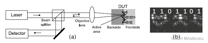
Fig. 1.5 Concept (a) and example (b) for laser voltage probing, which serves to read-out data/bits
in devices at runtime. In the example (b), an array of registers is in view, with those remaining
dark storing “0” and those lighting up storing “1.” Subfigure (a) is adopted from [Loh+16] and (b)
adopted from a related microscopy image provided as courtesy by Shahin Tajik
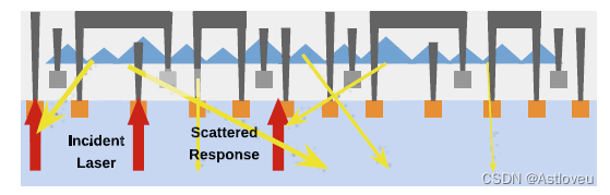
Fig. 1.6 Concept of pyramid structures in silicon substrate, e.g., achieved using dedicated etching
steps. As a result, reflections from incident laser light are scattered and intermingled, making a
distinct read-out of data more difficult. Adopted from [She+18]
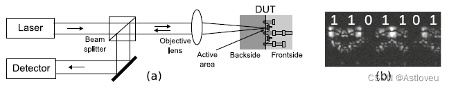
Fig. 1.5 激光电压探测的概念(a)和例子(b),其作用是在读取器件运行时的比特数据。在例子(b)中正在展现的是一组寄存器, 其中暗的单元存储的是比特“0”,亮的单元存储的是比特“0”。 子图(a)摘自[Loh+16],(b)来自由Shahin Tajik提供的相关显微图像。
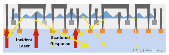
Fig. 1.6 硅基板中金字塔结构的概念,比如,可通过专用的蚀刻步骤实现。结果导致入射激光的反射光线被散射和混合,使得更加难以清晰地读出数据。摘自 [She+18]。
1.1.2 Securing the Integrity and Confidentiality of Hardware
Besides the severe threats on data security at runtime, as outlined above, other
threats such as reverse engineering (RE), piracy of chip-design intellectual property
(IP), illegal overproduction, counterfeiting, or insertion of hardware Trojans
represent further challenges for hardware security. These threats arise due to the
globalized and distributed nature of modern supply chains for electronics, which
span across many entities and countries. See also Fig. 1.7 for an overview of related
threats.
A multitude of protection schemes have been proposed, which can be broadly
classified into IP protection, Trojan defense, and physically unclonable functions
(PUFs). IP protection can be further broadly classified into logic locking, camouflaging,
and split manufacturing. All these schemes seek to protect the hardware
from different attack scenarios, which include untrusted foundries, untrusted testing
facilities, untrusted end-users, or a combination thereof. For example, selected
techniques for IP protection are illustrated in Table 1.1 along with the related
untrusted entities.
1.1.2 确保硬件的完整性与机密性
除了上述对运行时数据安全的严重威胁之外,其他威胁,如逆向工程(RE)、针对芯片设计知识产权(IP)的盗版、非法过度生产、伪造或植入硬件木马程序等都构成了对硬件安全的进一步挑战。这些威胁的源于现代电子产品供应链的全球化和分布式性质,它使得供应链横跨众多实体和国家。另请参见图1.7以了解相关威胁的概述。
针对上述威胁,业界已经提出了众多保护方案,大致可以分为知识产权保护、木马防御,以及物理不可克隆函数
(PUFs)三大类。知识产权保护技术可以进一步大致分为逻辑锁定、伪装和拆分制造三类。所有这些方案都是为了保护不同的硬件
攻击场景,其中包括不受信任的代工厂、不受信任的测试设施、不受信任的最终用户或上述场景的组合。例如,表1.1描述了一些所选知识产权保护的技术,以及与之相关的不受信任实体。

Fig. 1.7 An overview on design-, hardware-, and logistics-centric attacks throughout the (largely
outsourced) supply chain of modern electronics. Adopted from [Ber16]
Table 1.1 IP protection techniques versus untrusted entities (✓: Protection offered, ✗: No
protection offered)

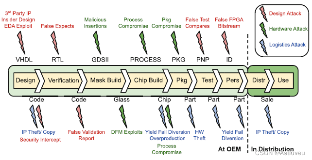
Fig. 1.7 对整个(主要是外包的)现代电子产品供应链中以设计、硬件和物流为中心的攻击的概述。外包)。摘自[Ber16]
Table 1.1 应对不受信任实体的知识产权保护方案 (✓: 可提供保护, ✗: 无法提供保护)
| 技术 | 前道工序/后道工序代工 | 测试实施 | 最终用户 |
|---|---|---|---|
| 逻辑锁定 | ✓/✓ | ✓ (参见 [Yas+16a]) | ✓ |
| 布局伪装 | ✗/✗ (✓/✗ [Pat+17, Pat+20a],✓/✓ [Ran+20a]) | ✗ (✓ [Ran+20a]) | ✓ |
| 拆分制造 | ✓/✗ (✗/✓ [Wan+17c]) | ✗ | ✗ (✓ [Pat+19a]) |
1.1.2.1 Logic Locking
Logic locking protects the design IP by inserting dedicated key-gates, which are
operated by a secret key [YRS20]. Without the knowledge of the secret key,
logic locking ensures that the details of the design IP cannot be fully recovered
and the IC remains non-functional. The key-gates are commonly realized
using, e.g., XOR/XNOR gates [RKM10], AND/OR gates [Dup+14], or look-up
tables (LUTs) [BTZ10]. Only after manufacturing (preferably even after testing
[Yas+16a]) is the IC to be activated, by loading the secret key into a dedicated,
on-chip tamper-proof memory. The realization of such tamper-proof memories
remains a topic of active research and will be covered in more detail in Chap. 7.
1.1.1.3 逻辑锁定
逻辑锁定是通过插入专用的密钥门(key-gates)来保护设计 IP,而这些门电路需要通过密钥 [YRS20] 来操作。只要密钥未泄露,逻辑锁定可确保设计IP的细节无法完全恢复,且集成电路不能正常工作。密钥门逻辑通常可通过异或/同或门 (XOR/XNOR)[RKM10]、与/或门(AND/OR ) [Dup+14] 或查找表 (LUTs) [BTZ10]来实现。IC只有在制造之后(最好是在测试之后[Yas+16a]) 才能被激活,方法是将密钥加载到专用的片上防篡改存储器中。如何实现这种防篡改的存储机制仍然是一个积极的研究课题,并将在第7章中更详细地介绍。
Threat Model In general, a threat model describes the capabilities of the attacker
and the resources at their disposal. It also classifies entities as trusted or untrusted.
The threat model for logic locking can be summarized as follows:
• The design house, designers, and the electronic design automation (EDA) tools
the designers work with are considered trusted, whereas the foundry, the test
facility, and the end-user(s) are all considered untrusted.
• The attackers possess knowledge regarding the logic locking technique that has
been applied to protect the design IP.
• The attackers have access to the locked netlist (e.g., by RE). Hence, they can
identify the key inputs and the related logic but are oblivious to the secret key.
• The secret key cannot be tampered with, as it is programmed in a tamper-proof
memory.
• The attackers are in possession of a functional chip bought from the open market.
This chip can act as an “oracle” for evaluating input/output patterns.
Without knowledge of the secret key, logic locking ensures that: (1) the details
of the original design cannot be fully recovered; (2) the IC is non-functional, i.e., it
produces incorrect outputs.
威胁模型 一般来说,威胁模型描述了攻击者的能力和其所掌握的资源。它还将实体分类为可信与不可信两类。
逻辑锁的威胁模型可以总结如下:
• 设计公司、设计师和电子设计自动化(EDA)工具被认为是可信的,而代工厂、测试机构和最终用户则
被认为是不可信的。
• 攻击者掌握有关用于保护设计 IP 的逻辑锁定技术的相关知识。
• 攻击者可以访问锁定的网表(例如,通过RE)。因此,他们可以识别关键的输入和相关的逻辑,但却对密钥却一无所知。
• 密钥被编程在防篡改存储器中,因此不能被篡改。
• 攻击者拥有一个从公开市场购买的功能芯片。该芯片可提供评估输入/输出模式的先验信息。
在攻击者不掌握密钥的情况下,逻辑锁定可以确保:(1) 原始设计的细节不能被完全恢复;(2) 集成电路处于无功能状态,即它会产生不正确的输出。
Logic Locking Techniques and Attacks Early research proposed random logic
locking (RLL) [RKM10], fault-analysis-based locking (FLL) [Raj+15], and strong
interference-based locking (SLL) [Raj+12], all to protect against brute force
attacks. These techniques identify suitable, selected locations for inserting the keygates.
However, multiple attacks have undermined the security guarantees of these
aforementioned techniques by formulating different attacks [Raj+12, PM15, LO19].
针对逻辑锁定技术和攻击的早期研究提出了随机逻辑锁定(RLL)[RKM10]、基于故障分析的锁定(FLL)[Raj+15],以及
基于强干扰的锁定(SLL)[Raj+12],都是为了防止暴力破解攻击。这些技术可用于识别可插入密钥门的合适的、选定的位置。
然而,当前已有多种攻击方式突破了上述技术的安全保障 [Raj+12, PM15, LO19]。
In 2015, Subramanyan et al. [SRM15] challenged the security promises of all
then-known logic locking techniques. This attack leveraged Boolean satisfiability
(SAT) to compute the so-called discriminating input patterns (DIPs). A DIP
generates different outputs for the same input across two (or more) different keys,
indicating that at least one of the keys is incorrect. The attack stepwise evaluates
different DIPs until all incorrect keys have been pruned. The attack experiences
its worst case scenario when it can eliminate only one incorrect key per DIP;
here, 2k − 1 DIPs are required to resolve k key bits. In general, the SAT attack resilience of any locking technique can be represented by the number of DIPs
required to decipher the correct key and the average time taken for each SAT attack
iteration [XS16].

Fig. 1.8 Selected SAT-resilient locking techniques: (a) SARLock, (b) Anti-SAT, © TTLock/SFLLHD,
and (d) SFLL-flex. Adopted from [YS17]
在2015年,Subramanyan等人[SRM15]挑战了当时所有已知的逻辑锁定技术。其攻击利用了布尔可满足性 (SAT)来计算所谓的可识别输入模式(DIP)。DIP 通过两个(或更多)不同的密钥为相同的输入生成不同的输出,且至少一个密钥是不正确的。攻击会逐步评估不同的DIP,直到所有不正确的密钥都被排除掉。在最坏的情况下,每个 DIP 仅能消除一个不正确的密钥,总计需要2k − 1 个 DIP 才能完成k位密钥的求解。 一般来说,针对任何锁定技术的SAT攻击的抵抗韧性都可以用破译正确密钥所需的DIP数量、以及单次SAT攻击迭代的平均耗时来表示[XS16]。
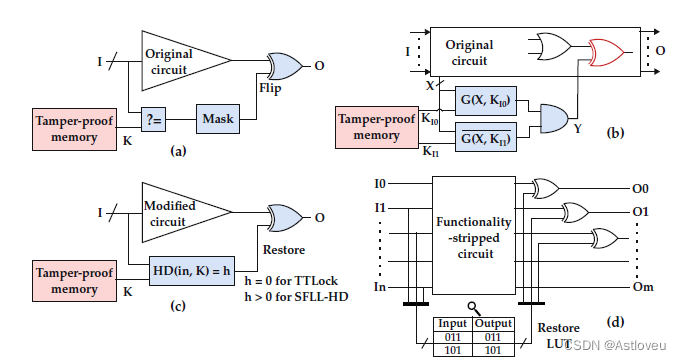
Fig. 1.8 选定的抗SAT的锁定技术: (a) SARLock, (b) Anti-SAT, © TTLock/SFLLHD,
以及(d) SFLL-flex. 摘自[YS17]
Initial research in SAT-resilient logic locking techniques aimed to increase the
complexity of the SAT-based attack by ensuring that the attack pruned out exactly
one incorrect key per iteration. To that end, in 2016, SARLock [Yas+16b] and
Anti-SAT [XS16] were put forward as defense techniques against the SAT-based
attack [SRM15]. SARLock (Fig. 1.8a) employs a controlled corruption of the output,
across all incorrect keys, for exactly one input pattern. SARLock can also be
integrated with other high-corruptibility techniques (e.g., FLL or SLL) to provide a
two-layer defense. In Anti-SAT [XS16], two complementary logic blocks, embedded
with the key-gates, converge at an AND gate (Fig. 1.8b). The output of this AND
gate is always “0” for the correct key; for the incorrect key, it may be “1” or “0,”
depending on the inputs. This AND gate then feeds an additional XOR gate that is
interposed into the original design, thereby possibly inducing incorrect outputs for
incorrect keys. Both techniques utilize the concept of point functions and enforce
low output corruptibility to obtain resilience against the SAT-based attack.
最初的抗SAT攻击的逻辑锁技术研究旨在通过确保攻击在每次迭代中仅能剪除一个错误密钥,来增加基于SAT的攻击的复杂度。每个迭代都有一个错误的密钥。为此,在2016年,SARLock[Yas+16b]和 Anti-SAT [XS16]作为防御SAT攻击的技术被首次提出[SRM15]。SARLock(图 1.8a)采用受控的输出损坏技术,其采用所有的错误密钥,对同一个输入模式进行控制性破坏。SARLock还可以与其他高破坏性技术(如FLL或SLL)集成,以实现双层防御。如图1.8b所示,在Anti-SAT[XS16]中,两个嵌入了密钥门的互补逻辑块,在一个与门处汇合。对于正确的密钥,该与门的输出总是 “0”;对于错误的密钥,输出可能是 "1 "或 “0”,具体取决于输入情况。然后,这个与门会给另外一个嵌入到原始设计中的异或门提供输入信息,从而使得错误的密钥导致错误的输出。这两种技术都是利用点函数的概念,并通过贯彻对输出的低可破坏性来获得对于SAT攻击的抵抗韧性。
The two-layer defense of SARLock was approximately circumvented by App-
SAT [Sha+18a] and Double DIP [SZ17]. In both the attacks, the combination of
a low-corruption part (resilient to SAT attacks) and a high-corruption part (prone
to SAT attacks) is reduced to the low-corruption part (e.g., SARLock + SLL to
SARLock). The Double DIP [SZ17] can eliminate at least two incorrect keys
in each iteration, thereby increasing the attack efficiency. For Anti-SAT, the two
complementary blocks at its heart exhibit significant signal skews, rendering them
distinguishable from other logic, which is exploited by Yasin et al. in the signal
probability skew (SPS) attack [Yas+16c]. Moreover, both SARLock and Anti-SAT are vulnerable to the bypass attack [Xu+17]. This attack picks some key randomly
and determines the inputs that provide incorrect outputs for this chosen key. Then,
additional logic is constructed around the Anti-SAT/SARLock blocks to recover the
overall circuit from these incorrect outputs.
SARLock的两层防御机制可被App-SAT [Sha+18a] 和 Double DIP [SZ17]绕过。在这两种攻击中,
低破坏性部分(对SAT攻击具有抵抗韧性)和高破坏性部分(易受SAT攻击)的组合被简化为低破坏性部分(例如,SARLock + SLL至SARLock)。Double DIP[SZ17]可在每个攻击迭代中至少排除两个错误密钥,从而提高攻击效率。对于Anti-SAT而言,其核心的两个互补逻辑块表现出明显的信号排查,使它们区别于其他逻辑,Yasin等人在信号概率偏移(SPS)攻击[Yas+16c]中利用了这一点。此外,SARLock和Anti-SAT都很容易遭受绕过攻击(bypass attack)[Xu+17]。这种攻击通过随机挑选密钥,并确定为此选定密钥提供错误输出的输入。然后,再围绕 Anti-SAT/SARLock 模块构建额外的逻辑,以利用这些错误的输出恢复出整体电路。
In TTLock, the original logic is modified for exactly one input pattern [Yas+17a].
The output for this protected pattern is restored using a comparator block, as
illustrated in Fig. 1.8c. Even if an attacker succeeds to remove the comparator
block, she/he obtains a design different from the original one (albeit for only one
input pattern). On the heels of TTLock, Yasin et al. [Yas+17b] proposed stripped
functionality logic locking (SFLL). SFLL is resilient against most current attacks,
and it enables one to trade-off between resilience against SAT attacks and removal
attacks [Yas+17b]. It is based on the notion of “strip and restore,” where some part
of the original design is removed and the intended functionality is concealed.
在 TTLock 中,原始逻辑只会针对一个输入模式 [Yas+17a] 实施修改。
如图 1.8c 所示,此受保护模式的输出可通过使用比较器模块来恢复。即使攻击者成功移除了比较器模
块,也只能获得与原始设计不同的信息(尽管只有一个输入模式)。在TTLock之后,Yasin等人[Yas+17b]提出了剥离
功能逻辑锁(SFLL)技术。SFLL可以抵御目前大多数的攻击。
它使人们能够在抵御SAT攻击和移除攻击[Yas+17b]之间进行权衡。SFLL技术基于 "剥离和恢复 "的概念,通过将原始设计的某些部分移除,从而隐藏预期的功能。
SFLL has three variants, SFLL-HD [Yas+17b], SFLL-flex [Yas+17b], and SFLL-rem
[Sen+20], which we briefly discuss next. SFLL-HD is a generalized version of
TTLock that allows the designer to protect a larger number of selected input patterns.
It should be noted that SFLL-HD protects a restricted set of input cubes, which
are all underpinned by one secret key. SFLL-flexc×k, in contrast, allows to protect
any c selected input cubes, each with k specified bits. Here, the protected patterns
are typically represented using a small set of input cubes, which are then stored
in an on-chip LUT (Fig. 1.8d). In SFLL-fault, fault-injection-based heuristics are
leveraged to identify and protect multiple patterns and to reduce area cost at the
same time. Both SFLL-HD and SFLL-flexc×k utilize AND-trees that leave structural
hints for an opportune attacker. Related attacks have been demonstrated by Sirone et
al. [SS19] and Yang et al. [YTS19], tackling these locking schemes without access
to an oracle. Recently, graph neural network-based unlocking techniques [Alr+20]
have been proposed to facilitate this notion of oracle-less recovery attacks as well.
The sparse prime implicant (SPI) attack [HYR21] was shown to break the security
guarantees of SFLL-rem [Sen+20].
SFLL有三个变体:SFLL-HD [Yas+17b], SFLL-flex [Yas+17b], 和SFLL-rem [Sen+20],接下来我们将简要讨论。
SFLL-HD是TTLock的一个通用版本,允许设计者保护更多的选定输入模式。值得注意的是,SFLL-HD保护的是一组有限的输入序列,且都由一个密钥支撑。相比之下,SFLL-flexc×k则允许保护任何c个选定的输入序列,每个序列有k个指定的比特位。在这里,被保护的模式通常用一小组输入序列来表示,然后将其存储在片上LUT中(图1.8d)。 在SFLL-fault中,基于故障注入的启发式方法被用来识别多种模式并降低芯片面积成本。SFLL-HD和SFLL-flexc×k都利用了"与"树(AND-tree)结构,为攻击者留下了结构化的提示。Sirone [SS19]与Yang[YTS19]等人[YTS19]已证实了相关攻击,可在在没有先验知识的情况下破解这些锁定方案。最近,基于图神经网络的解锁技术[Alr+20]也被提出,以促进此种非先验知识依赖性的破解攻击概念。稀质蕴含项(SPI)攻击[HYR21]被证明可以攻破SFLL-rem[Sen+20]的安全保证。
Further Defenses and Attacks Related to Logic Locking Shamsi et
al. [Sha+18b] presented a layout-centric logic locking scheme, based on routing
cross-bars comprising obfuscated and configurable vias. The notion of cyclic
locking has been proposed in [Sha+17b] and extended in [RMS18]. The idea
is to create supposedly unresolvable locking instances by introducing feedback
cycles. However, tailored SAT formulations have challenged such locking
schemes [ZJK17, She+19].
与逻辑锁定相关的进一步攻防技术:Shamsi [Sha+18b] 提出了一种以布局为中心的逻辑锁定方案,该方案基于由混淆后的可配置通孔组成的互连路由阵列。循环锁定的概念已在[Sha+17b]中提出,并在[RMS18]中得到了进一步扩展。该想法是通过引入反馈循环来创建假定无法求解的锁定实例。然而,通过定制的SAT公式可对此类循环锁定方案构成挑战[ZJK17, She+19]。
Recent works have proposed parametric locking [Yas+17a, XS17, Zam+18,
CXS18]; the essence is to lock design parameters and profiles. For example,
in [XS17], the key not only protects the functionality of the design but also
its timing profile. A functionally correct but timing-incorrect key will result in
timing violations, thereby leading to circuit malfunctions. A timing-based SAT
attack, presented in [CLS18], circumvented the timing locking approach in [XS17].
Therefore, further research into parametric locking is required. The notion of mixedsignal
locking has been advocated recently as well, e.g., in [Jay+18, Leo+19].
业界最近的研究工作提出了参数化锁定 [Yas+17a, XS17, Zam+18,
CXS18]的概念;其实质是锁定设计参数和保护轮廓。例如。
在[XS17]中,密钥不仅保护了设计功能,而且还保护了IC的时序轮廓。一个功能正确但定时不正确的密钥将导致
时序违规,从而导致电路故障。在[CLS18]中提出一种基于时间的SAT攻击,可规避[XS17]中描述的时间锁定方法。
因此,有必要对参数化锁定进行进一步研究。同时,最近业界也在提倡混合信号锁定的概念,例如[Jay+18, Leo+19]。
Finally, further attack/defense schemes on regular locking techniques have been
proposed that focus on inferring/obfuscating the structural modifications induced
by locking, without requiring an oracle, e.g., [CCB18, Alr+21].
最后,关于常规锁定技术的进一步攻防方案已被提出,其重点是干扰/混淆由锁定引起的结构性修改,且
不依赖先验知识,例如[CCB18, Alr+21]。
1.1.2.2 Layout Camouflaging
Layout camouflaging serves to mitigate RE attacks conducted by malicious endusers.
Broadly speaking, layout camouflaging alters the layout-level appearance of
an IC in order to protect the design IP. As illustrated in Fig. 1.9, layout camouflaging
can be achieved by dedicated front-end-of-line (FEOL) processing steps, like
manipulation of dopant regions, gate structures, and/or gate contacts [Raj+13a,
Erb+16, Li+16], but also by obfuscation of the back-end-of-line (BEOL) interconnects
[Pat+17, Pat+20a]. Layout camouflaging has been made available for
commercial application, e.g., see the SypherMedia Library [Ram19]. Note that
obfuscation is also known in the context of design-time protection, e.g., by
obfuscating finite state machines [LP15]—such techniques are orthogonal to layout
camouflaging.
1.1.2.2 布局伪装
布局伪装用于减轻恶意最终用户发起的逆向攻击(RE)。从广义上讲,布局伪装可改变 IC 的布局层面外观,以保护设计 IP。
如图1.9所示,布局伪装可通过特定的前道工序(FEOL)处理步骤来实现,例如针对
掺杂区域、栅极结构和/或栅极触点的操纵[Raj+13a, Erb+16, Li+16],以及通过混淆后端工序(BEOL)的互连来实现 [Pat+17, Pat+20a]。布局伪装技术已商用,例如,可参见SypherMedia库[Ram19]。值得注意的是,混淆技术也常用于IC设计阶段的IP保护,例如,通过混淆有限状态机[LP15]来实施IP保护,这些技术手段与布局伪装是正交的,不存在冲突。
Threat Model The threat model for layout camouflaging is summarized as follows:
• The design house and foundry are trusted, the test facility is either trusted or
untrusted, and the end-user is untrusted.
• The adversary holds one or multiple functional chip copies and is armed with
sophisticated equipment and know-how to conduct RE. The resilience of any
camouflaging scheme ultimately depends on the latter.
• The adversary is aware of the camouflaging scheme, and she/he can identify
the camouflaged gates, infer all the possible functions implemented by the
camouflaged cell, but cannot readily infer the actual functionality.
威胁模型 布局伪装技术的威胁模型可总结如下:
• IC设计和代工机构是可信的,测试机构要么可信、要么不可信,而终端用户是不可信的。
• 攻击者拥有若干个功能完备的IC芯片,并掌握并配备了先进的设备与技术来实施逆向攻击。任何
伪装方案的防御韧性最终取决于后者(攻击者的能力和所掌握的资源)。
• 攻击者了解具体的伪装方案,并可以识别出伪装后的门电路、推断出由伪装单元实现的所有功能,但无法轻易推断出实际功能。
Layout Camouflaging Techniques and Attacks Similar to logic locking, early
studies focused on the selection of gates to camouflage (and the design of camouflaged
cells). In their seminal work, Rajendran et al. [Raj+13a] proposed
a camouflaged NAND-NOR-XOR cell. The authors also proposed clique-based selection for camouflaging, based on their own finding that a random selection of gates to camouflage can be resolved by sensitization-based attacks [Raj+13a].
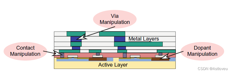
Fig. 1.9 Device-level concepts for layout camouflaging
布局伪装技术及相关攻击与逻辑锁定类似,早期的研究集中在如何选择伪装的门电路以及伪装单元的设计。Rajendran等人在其开创性工作[Raj+13a]z中提出了一种伪装的"与非-非-异或(NAND-NOR-XOR)"单元。作者还发现可通过基于敏感度的攻击来破解对伪装门电路的随机选择,并基于该发现进一步提出了基于派系(clique) 的伪装选择方法[Raj+13a]。

Fig. 1.9 布局伪装的器件级概念
Massad et al. [MGT15] and Yu et al. [Yu+17] independently formulated
SAT-based attacks (with oracle access), which challenged the security guarantees
of [Raj+13a]. These attacks could readily circumvent small-scale camouflaging
for various benchmarks with up to 256 gates being camouflaged. A parallel
SAT-based attack providing an average speedup of 3.6× over prior attacks was
presented by Wang et al. [Wan+18a]. Keshavarz et al. [Kes+18] proposed a SATbased
formulation augmented by probing and fault-injection capabilities, where the
authors were able to RE an S-Box. Still, it remains to be seen whether the attack can
tackle larger designs.
Massad等人[MGT15]和Yu等人[Yu+17]各自独立制定了基于SAT的攻击方法(依赖先验知识),并对[Raj+13a]中承诺的安全保证提出了挑战。这些攻击很容易绕过不超过256个门电路规模的伪装。Wang等人[Wan+18a]提出了一种基于SAT的并行攻击方法,比之前的攻击平均提速3.6倍。Keshavarz等人[Kes+18]也提出了一种基于SAT的攻击方法,该方法得益于探测和故障注入,通过该方法,作者成功实现了对一个S-Box的逆向攻击。不过,这种攻击是否能对更大规模的设计构成威胁,还有待于进一步观察。
In [YSR17], Yasin et al. demonstrated how an untrusted test facility can
circumvent the security promise of camouflaging, even without access to an oracle.
The authors deciphered the layout camouflaging technique presented in [Raj+13a]
successfully by analyzing the test patterns provided by the design house to the
untrusted test facility. To the best of our knowledge, none of the layout camouflaging
techniques proposed thus far have been able tomitigate this kind of attack, except for
the dynamic camouflaging technique presented in [Ran+20a], which is discussed in
more detail in Chap. 3.
在[YSR17]中,Yasin等人证明了不受信任的测试机构即使在没有先验知识的前提下,如何能够绕过伪装技术的防护并实施攻击。
作者通过分析设计公司提供给测试机构的测试模式,成功破译了[Raj+13a]中提出的布局伪装技术。据我们所知,除了 [Ran+20a]中提出的动态伪装技术,迄今为止提出的所有布局伪装技术都无法应对此类攻击。关于动态伪装技术,将在第三章中详细讨论。
Many existing layout camouflaging techniques, e.g., [Raj+13a, Nir+16,
CMG16, Wan+16a], exhibit a significant cost with respect to power, performance,
and area (PPA). For example in [Raj+13a], camouflaging 50% of the design results
in ≈150% overheads for power and area, respectively. See Fig. 1.10 for an analytical
experiment on layout costs for camouflaging versus split manufacturing (introduced
in the next subsection). A more comprehensive investigation of PPA cost for various
layout camouflaging techniques is provided in [Pat+17, Pat+20a].
许多现有的布局伪装技术,例如,[Raj+13a, Nir+16, CMG16, Wan+16a],在功耗性能面积(PPA)方面都存在较大的开销。以[Raj+13a]为例,对50%的设计进行伪装会导致功率和面积方面分别大约150%的额外开销。关于伪装与拆分制造技术(拆分制造技术将在下一节中介绍)在布局开销上的的分析对比实验,可参考图 1.10。针对各种布局伪装技术在PPA开销方面的更全面的调查,可参见[Pat+17, Pat+20a]。

Fig. 1.10 Study on PPA cost (%) for layout camouflaging [Raj+13a] (left) and lifting of wires
(randomly selected) to M8 (metal layer 8) for split manufacturing (right). Results are averaged
across ITC-99 benchmarks. For layout camouflaging (left), the impact on power and area is
substantial, given that the NAND–NOR–XOR structure proposed in [Raj+13a] incurs 4× and
5.5× more area and power compared to a regular 2-input NAND gate. For split manufacturing
(right), the cost for area is severe; that is because routing resources are relatively scarce for
M8 (pitch = 0.84μm) and lifting of wires occupies further routing resources, which can only be
obtained by enlarging the die outlines
Fig. 1.10 针对布局伪装技术[Raj+13a](左)与拆分制造技术(右,通过随机将连线拉至M8层(metal layer 8)来实现)在PPA方面的开销(%)研究。测试结果采用针对 ITC-99基准电路的平均值。布局伪装技术(左图)在功率和面积方面存在较大开销,
[Raj+13a]中提出的NAND-NOR-XOR结构与普通的2路输入信号的与非门相比,前者的面积和功率消耗分别是后者的4倍与5.5倍。拆分制造 (右图)技术的面积成本很高;这是因为M8层(间距=0.84μm)的走线资源相对匮乏,而拉线会占用更多的走线资源,只能通过扩大芯片的轮廓来获得。
Most layout camouflaging techniques also require modifications in the frontend-
of-line (FEOL) manufacturing process, which can incur financial cost on top
of PPA overheads. Therefore, in such scenarios, layout camouflaging is applied
selectively, to limit PPA cost and the impact on FEOL processing. However, the
selective application of layout camouflaging techniques compromises the security
guarantees, especially in the light of oracle-guided SAT attacks such as [MGT15,
Yu+17, Wan+18a].
大多数布局伪装技术也需要修改前道工序(FEOL)的制造工艺,这可能会导致PPA开销之外的额外财务成本。因此,在此种情况下,布局伪装常被选择性地应用,以限制对PPA开销以及FEOL工艺的影响。然而,选择性应用布局伪装技术也会损害安全保证,
尤其是面对诸如[MGT15, Yu+17, Wan+18a]等基于先验知识引导的SAT攻击时。
The notion of provably secure layout camouflaging was put forward
in [Yas+16d, Li+16]. CamoPerturb [Yas+16d] seeks to minimally perturb the
functionality of the design by either removing or adding one minterm (i.e., the
product term of all variables). A separate block, called CamoFix, is then added to
restore the minterm; CamoFix is built up using camouflaged INV/BUF cells. This
concept is inherently similar to the idea of TTLock, which was discussed previously.
Inspired by logic locking, Li et al. [Li+16] employ AND-trees as well as OR-trees
for layout camouflaging. Depending on the desired security level, tree structures
inherently present in the design are leveraged, or additional trees are inserted. Then,
the inputs of the trees are camouflaged using dopant-obfuscated cells.
[Yas+16d, Li+16]中提出了可证明安全布局伪装的概念。CamoPerturb [Yas+16d]试图通过删除或增加一个最小项(即所有变量的乘积项)来实现对设计功能的最低限度加扰。然后通过添加一个称为CamoFix的单独模块来恢复上述最小项,而CamoFix是用伪装的逆变器/缓冲(INV/BUF)单元创建的。这个概念在本质上与之前讨论的TTLock类似。受逻辑锁的启发,Li等人[Li+16]采用了“与”树(AND-tree)和“或”树(OR-tree)结构来进行布局伪装。根据所需的安全级别,可充分利用设计中固有的树状结构,或插入额外的树状结构。接下来,树的输入信号会通过使用掺杂混淆(dopant-obfuscated)单元来伪装。
Both techniques [Yas+16d, Li+16] have been shown to exhibit vulnerabilities:
[Li+16] was circumvented by sensitization-guided SAT attack (SGS) [Yas+17c],
while Jiang et al. [Jia+18] circumvented CamoPerturb using sensitization and
implication principles leveraged from automated test pattern generation (ATPG).
In general, these techniques are also vulnerable to approximate attacks outlined
in [Sha+17a, Sha+18a]. A follow-up work to [Li+16] is presented in [Li+17],
where the authors discuss how structural attacks like SPS [Yas+16c] can be
rendered ineffective when the trees are obfuscated both structurally and functionally.
However, such structural and functional obfuscations are also vulnerable to
sophisticated attacks.
[Yas+16d, Li+16]中描述的两种技术都已被证明存在漏洞。其中,[Li+16]的防御机制可通过敏化引导的SAT攻击(SGS)[Yas+17c]来绕过,而Jiang等人[Jia+18]则利用自动测试模式生成(ATPG)中的敏化和暗示原则绕过了CamoPerturb [Yas+16d]的防御机制。一般来说,这些技术也容易遭受[Sha+17a, Sha+18a]中概述的近似攻击。
[Li+17] 介绍了[Li+16] 后续工作,其中,作者讨论了当树在结构和功能上都被混淆时,像 SPS [Yas+16c] 这样的结构攻击是如何失效的。然而,这种结构和功能上的混淆也很容易遭受复杂攻击。
Further Defenses and Attacks Related to Layout Camouflaging Besides the
various analytical attacks, RE may also compromise layout camouflaging techniques
directly. For example, ambiguous gates [Raj+13a, Coc+14] or secretly
configured MUXes [Wan+16a] rely on dummy contacts and/or dummy channels,
which will induce different charge accumulations at runtime. Courbon et
al. [CSW16] leveraged scanning electron microscopy in the passive voltage contrast
mode (SEM PVC) for measurement of charge accumulations, where they succeeded
in reading out a secured memory. Furthermore, monitoring the photon emission at
runtime can presumably also help uncover layout camouflaging [Loh+16].
与布局伪装相关的进一步防御与攻击 除了各种分析性攻击之外,通过逆向工程也可以直接攻破布局伪装技术。例如,无论是模糊逻辑门[Raj+13a, Coc+14]还是秘密配置的多路复用器 [Wan+16a],均依赖于虚拟触点或虚拟通道,将在运行时引起差异化的电荷积累。Courbon等人[CSW16]利用扫描电子显微镜的被动电压对比(SEM PVC)来测量电荷积累,并成功地读出了一个安全存储器中的内容。此外,通过监测运行时的光子发射,想必也能帮助破解布局伪装[Loh+16]。
Threshold voltage-based layout camouflaging (TVC) has gained traction over
the past few years. The essence of TVC is a selective manipulation of dopants
at the transistor level that creates logic cells that are identical structurally but
depict different functionalities. Nirmala et al. [Nir+16] proposed TVC cells that
can operate as NAND, NOR, OR, AND, XOR, or XNOR. Erbagci et al. [Erb+16]
proposed TVC cells operating as XOR or XNOR, based on the selective use of highand
low-threshold transistors. Collantes et al. [CMG16] adopted domino logic to implement their TVCs. Recently, Iyengar et al. [Iye+18] demonstrated two flavors of TVC in STMicroelectronics 65 nm technology. In principle, TVC techniques
offer better resilience than other layout camouflaging techniques, as regular etching
and optical imaging techniques are ineffective with respect to TVC. Still, TVC may
be revealed eventually, e.g., by leveraging SEM PVC [Sug+15].
基于阈值电压的布局伪装(TVC)在过去的几年里获得了广泛的关注。TVC技术的本质是在晶体管层面有选择地实施掺杂
,以创造出结构上相同但功能上不同的逻辑单元。 Nirmala等人[Nir+16]提出的TVC单元可以执行"与非"、“非”、"或‘、“与”、“异或” 或者"同或"等多种逻辑运算之一。Erbagci等人[Erb+16] 基于对高和低阈值晶体管的选择性使用,提出了以"异或"或"同或"方式工作的TVC单元。而Collantes等人[CMG16]则采用多米诺逻辑(domino logic)来实现其TVC。最近,Iyengar等人[Iye+18]在意法半导体(STMicroelectronics)的65纳米技术中展示了两种类型的TVC。不过,TVC伪装最终也可能会被揭开,例如,通过利用扫描电子显微镜的被动电压对比(SEM PVC) [Sug+15]作为破解手段。
Another interesting avenue is the camouflaging of the back-end-of-line (BEOL),
i.e., the interconnects [Che+15, Pat+17, Pat+20a, Jan+18]. Chen et al. [Che+15,
CCW18] explored the use of real vias (magnesium, Mg) along with dummy vias
(magnesium oxide, MgO) to achieve the same. They have shown that Mg can
oxidize quickly into MgO, thereby hindering an identification by an RE attacker.
Recently, Patnaik et al. [Pat+17, Pat+20a] extended the concept of BEOL camouflaging
in conjunction with split manufacturing, to protect against an untrusted
FEOL foundry. Patnaik et al. developed customized cells and design stages for
BEOL camouflaging, where they successfully demonstrated full-chip camouflaging
at lower PPA cost than prior works. Their study also explored how large-scale
(BEOL) camouflaging can thwart SAT-based attacks, by inducing overly large and
complex SAT instances, which overwhelm the SAT solvers.
为了实现伪装,另外一种有趣的途径是借助后道工序(BEOL)的布线互连处理[Che+15, Pat+17, Pat+20a, Jan+18]。Chen等人[Che+15, CCW18]探讨了使用真通孔(材料为镁,Mg)与假通孔 (材料为氧化镁,MgO)来实现这一目标。他们已证实,金属镁可以迅速氧化成为氧化镁,从而阻碍了逆向攻击的破解。最近,Patnaik等人[Pat+17, Pat+20a]扩展了BEOL伪装的概念,并将其与拆分制造技术相结合,以抵御来自不受信任的前道工序( FEOL)代工机构的威胁。Patnaik等人开发了定制化的单元与设计阶段,用于BEOL伪装。基于此,他们成功地展示了全芯片级的伪装,且该成果比之前的工作具有更低的PPA开销。在研究中,他们还探讨了大规模BEOL伪装是如何通过诱导生成巨大复杂的SAT实例,使得SAT求解器不堪重负,从而挫败基于SAT的攻击。
Most techniques discussed so far cannot be configured post-fabrication, i.e., they
implement static camouflaging. In contrast, Akkaya et al. [AEM18] demonstrated
a reconfigurable camouflaging scheme that leverages hot-carrier injection. Notably,
the authors fabricated a prototype in 65 nm technology; however, they report significant
PPA cost (e.g., in comparison to regular NAND gates, they report 9.2×, 6.6×,
and 7.3× for power, performance, and area, respectively). Zhang et al. [Zha+18a]
introduced the concept of timing-based camouflaging, based on wave-pipelining and
false paths. However, this technique was circumvented in [Li+18b].
迄今为止,本文所讨论的大多数技术都不支持在IC制造后通过重构进行变更,也就是说,它们实施的保护类型都属于静态伪装。
与此相反,Akkaya等人[AEM18]展示了一种利用热载波注入的可重构伪装方案。值得注意的是,作者基于65纳米技术制造了一个原型;然而,他们也揭示了该方案具有显著的PPA开销(例如,与常规NAND门相比,此原型的功率、性能和面积分别为其9.2倍、6.6倍。和7.3倍)。Zhang等人[Zha+18a] 介绍了基于时序的伪装概念,基于波流水线(wave-pipelining)和 虚假路径技术。然而,该技术的防御可被[Li+18b]中描述的攻击方法绕过。
1.1.2.3 Split Manufacturing
Split manufacturing seeks to protect the design IP from untrustworthy
foundries [RSK13, Sen+17, Pat+18e, Pat+18f, McC16, Pat+21]. As indicated
by the term, the idea is to split the manufacturing flow, most commonly into an
untrusted FEOL process and a subsequent, trusted BEOL process (Fig. 1.11).
Such splitting into FEOL and BEOL is practical for multiple reasons:
• Outsourcing the FEOL is desired, as it requires some high-end and costly
facilities.
• BEOL fabrication on top of the FEOL is significantly less complex than FEOL
fabrication itself.
• Some in-house or trusted third-party facility can be engaged for BEOL fabrication.
• The sole difference for the supply chain is the preparation and shipping of FEOL
wafers to that facility for BEOL fabrication.
1.1.2.3 拆分制造
拆分制造旨在保护设计IP免于来自不可信的代工厂的威胁[RSK13, Sen+17, Pat+18e, Pat+18f, McC16, Pat+21]。正如该术语(Split Manufacturing)所示,此想法是将制造流程拆分开来,最常见的是将其分为不可信的前道工序(FEOL)和后续可信的后道工序(BEOL)(如图1.11所示)。出于以下多种原因,这种拆分为 FEOL 和 BEOL 的做法是可行的:
• 将 FEOL外包是必要的,因为需要依赖一些高端且昂贵的设备进行处理。
•在 FEOL基础上的BEOL, 其制造过程的复杂度明显低于FEOL。.
• 可聘请一些内部或可信赖的第三方架构实施BEOL制造。
• 对供应链而言,唯一的区别是在完成FEOL工序后,还需将半成品晶片运输至BEOL制造机构。
In fact, split manufacturing has been demonstrated successfully; [Vai+14a]
describes promising results for a 130 nm process split between IBM and Global-Foundries, and [McC16] reports on a 28 nm split process run by Samsung across Austin and South Korea.

Fig. 1.11 Classical split manufacturing, i.e., the separation into front-end-of-line (FEOL) and
back-end-of-line (BEOL) parts
事实证明,拆分制造的模式在业界是成功的;[Vai+14a]描述了IBM与全球各代工厂之间关于130纳米制造工艺拆分的良好效果与前景;[McC16]也报道了三星在奥斯汀与韩国之间对28纳米制造工艺进行拆分的实践。
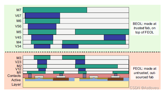
Fig. 1.11 经典的拆分制造过程,即分为前道工序(FEOL)和后道工序(BEOL)两部分。
Regarding the security notion of split manufacturing, a split layout appears to an
adversary in the FEOL facility as a “sea of incomplete gates and wires,” making it
challenging to infer the entire netlist, its design IP, and ultimately the functionality.
Still, given that regular, security-agnostic design tools work holistically on both the
FEOL and BEOL, hints on the missing wiring can remain in the FEOL [Wan+16b,
Li+19], which can be exploited by attackers, to decipher the missing connections.
关于拆分制造的安全概念,对攻击者而言,拆分后的布局意味者 “海量且不完整的门电路与线路”,这使得推断出整个网表、设计IP乃至芯片的最终功能的任务变得极具挑战性。尽管如此,鉴于与安全无关的常规设计工具整体上在
FEOL 和 BEOL上都有使用,有关缺失线路的线索仍可保留在 FEOL [Wan+16b,Li+19]中,攻击者可以利用这些线索来破译丢失的连接信息。
Threat Model The basic, most common threat model for split manufacturing is
summarized as follows:
• The design house and end-user are trusted, while the FEOL foundry is deemed
untrustworthy. Split manufacturing necessitates a trusted BEOL foundry, with
assembly and testing facilities typically also considered as trustworthy. The enduser
is also considered trustworthy (e.g., defense establishments).
• With the design house and end-user being trusted, the adversary cannot obtain
a chip copy from those entities. Besides, the chip has typically not been
manufactured before; the chip is then unavailable altogether for RE attacks.
• The primary goal of the adversary is to infer the missing BEOL connections
from the incomplete FEOL layout. Once the attacker deciphers all the missing
connections correctly, he/she can pirate and/or illegally overproduce the design
IP. To that end, she/he (1) is aware of the underlying protection technique, if any,
and (2) has access to the EDA tools, libraries, and other supporting information.
威胁模型 拆分制造的最基本常见的威胁模型可归纳如下:
• 设计公司和终端用户是可信的,而FEOL代工厂则被认为是不可信的。拆分制造需要可信的BEOL代工厂,装配和测试机构通常也被认为是可信的。且终端用户也被认为是可信的(例如,国防机构)。.
• 由于设计公司和最终用户是可信的,攻击者无法从这些实体获得芯片拷贝。此外,由于该芯片在历史上通常没有被制造过,故无法利用实体芯片实施逆向攻击。
•攻击者的主要目标是从不完整的FEOL布局中推断出缺失的BEOL线路连接。一旦攻击者正确破解了所有缺失的连接,他就可以掌握设计IP并进行盗版生产。为此,他首先必须了解所用的基本保护技术(如果有的话),而且还要有机会获得EDA工具、库和其他的支持信息。
An “inverted threat model” was explored in [Wan+17c], where the BEOL
facility is untrustworthy and the FEOL fab is trustworthy. Since fabricating the FEOL is more costly than the BEOL, the practical relevance of this model remains questionable.
在[Wan+17c]中探讨了一个 “倒置的威胁模型”,其中BEOL代工厂是不可信的,而FEOL代工厂是可信的。由于FEOL的制造成本比BEOL高,这个模型的实际意义仍然值得怀疑。
Another variation of the threat model was explored recently by Chen and
Vemuri [CV18b]. The authors assume that a working chip is available, which is
then used as an oracle for a SAT-based formulation to recover the missing BEOL
connections. While it is not explicitly stated in [CV18b], we presume that the
authors seek to recover the gate-level details of some design whose functionality
is otherwise already available/known. For an attacker, doing so can be relevant, e.g.,
for inserting hardware Trojans during re-implementation of some existing design,
or to obtain the IP without RE of the available chip copy.
Chen和Vemuri[CV18b]最近研究了此威胁模型的另一个变体。作者假设攻击者掌握了一个可用的芯片,然后将其作为基于SAT公式求解的先验信息,用以破解缺失的BEOL连接。虽然在[CV18b]中没有明确阐述,但我们推测作者针对一些已知功能的设计,试图恢复其门电路级细节。对攻击者而言,这样做可以达成多种相关目的,例如在重构现有设计的过程中插入硬件木马、或者无需通过针对实体芯片的逆向破解就可掌握设计IP。
Imeson et al. [Ime+13a] further proposed a strong model in the context of
hardware Trojans. Here, the attacker already holds the design netlist and is interested
in inserting Trojans in appropriate locations. This work [Ime+13a], also known as
k-security, has been further extended in [Li+18a].
Imeson等人[Ime+13a]在硬件木马的背景下进一步提出了一个增强的威胁模型。在此模型中,攻击者已经掌握了设计网表,并试图在适当的位置插入硬件木马。这项工作[Ime+13a]也被称为 k-security,并在[Li+18a]中被进一步研究拓展。
Split Manufacturing Techniques and Attacks The first attack on split manufacturing
was proposed by Rajendran et al. [RSK13]. The notion of this so-called
proximity attack is as follows. Although the layout is split into FEOL and BEOL, it is
still designed holistically (when using regular EDA tools). Rajendran et al. [RSK13]
infer the missing connections in the BEOL from the proximity of cells, which
is readily observable in the FEOL. While this attack shows a good accuracy for
small designs, the same is not true for larger designs. Wang et al. [Wan+16b]
extended this attack, by taking into account a multitude of FEOL-level hints:
(1) physical proximity of gates, (2) avoidance of combinatorial loops (which are
rare in practice for combinational designs), (3) timing and load constraints, and
(4) directionality of “dangling wires” (i.e., the wires remaining unconnected in the
top-most FEOL layer). Magaña et al. [MSD16] proposed various routing-based
attack techniques and conclude that such attacks are more effective than solely
placement-centric attacks. Recently, Zhang et al. [ZMD18] and Li et al. [Li+19]
leveraged machine learning techniques for deciphering missing connections. However,
neither attack [MSD16, ZMD18, Li+19] recovers the actual netlist; rather,
they provide the most probable BEOL connections.
拆分制造技术与相关攻击 首个针对拆分制造的攻击是由Rajendran等人提出的[RSK13]。这种所谓的接近式攻击(proximity attack)的概念为:虽然布局被分割成FEOL和BEOL,但基于常规EDA工具,IC设计依然是一个整体工作。由此,Rajendran等人[RSK13] 提出可通过单元间的接近程度推断出BEOL中缺失的连接,而这一点在FEOL中很容易观察得到。虽然这种攻击对小型设计显示出良好的准确性,但对于规模较大的设计而言,效果却欠佳。因此,Wang等人[Wan+16b]通过采用大量FEOL级别的提示线索来扩展此种攻击,具体包括:(1) 门电路间的物理接近度, (2) 对于组合循环设计的规避(这在组合设计的实践中相当罕见) (3) 时序和负载的限制, 以及(4) 悬空线的方向性(即在FEOL最上层中尚未连接的线路)。Magaña等人[MSD16]提出了多种基于绕线的攻击技术,并得出结论,此类攻击比单纯的以布局为中心的攻击更有效。
On the defense side, various techniques have been proposed to safeguard FEOL
layouts against proximity attacks, e.g., [RSK13, Vai+14b, Wan+16b, Sen+17,
Wan+17d, MSD16, Fen+17, Pat+18e, Pat+18f, CV18a, Li+20, Pat+21]. They
can be categorized into (1) placement-centric, (2) routing-centric, and (3) both
placement- and routing-centric defenses.
在防御方面,业界已提出了多种保护FEOL
布局的技术,例如,[RSK13, Vai+14b, Wan+16b, Sen+17,
Wan+17d, MSD16, Fen+17, Pat+18e, Pat+18f, CV18a, Li+20, Pat+21] 。
它们可以分为 (1) 以布局为中心,(2) 以绕线为中心,以及 (3) 同时以布局和绕线为中心的防御类别。
Wang et al. [Wan+16b] and Sengupta et al. [Sen+17] propose placement
perturbation. Layout randomization is the most secure technique, especially when
splitting after the first metal layer, as shown by Sengupta et al. [Sen+17]. However,
this technique has limited scalability and demonstrates significant layout cost for
larger designs. In general, placement-centric works caution that splitting after
higher metal layers—which helps to limit financial cost and practical hurdles for
split manufacturing [XFT15, Pat+18e, Pat+18f, Pat+21]—can undermine their resilience. That is because any placement perturbation is eventually offset by routing
at higher layers.
Wang[Wan+16b]与Sengupta等人[Sen+17]提出布局扰动(placement perturbation)的概念。将布局随机化是最为安全的技术,尤其是如Sengupta等人[Sen+17]所示,在第一金属层之后进行拆分处理时。然而,此类技术的可扩展性有限,对于较大规模的设计而言,布局开销显著增长。总体而言,针对以布局为中心的技术,如果在较高的金属层之后实施制造工艺的拆分,一方面
会有助于控制制造的财务成本、减少制造过程中的实际障碍[XFT15, Pat+18e, Pat+18f, Pat+21],另一方面会也破坏该技术的弹性和扩展性,这是因为针对任何位置的扰动最终都会被更高层的绕线所抵消。
Routing-centric techniques such as those in [RSK13, Wan+17d, MSD16,
Fen+17, Pat+18e, Li+20, Pat+21] resolve proximity and other hints at the FEOL
routing. Rajendran et al. [RSK13] proposed to swap pins of IP modules and to
re-route those nets, thereby obfuscating the design hierarchy. As these swaps cover
only part of the interconnects, this technique cannot protect against gate-level IP
piracy. In fact, 87% of the connections could be correctly recovered on the ISCAS-
85 benchmarks [RSK13]. In general, routing-centric techniques are subject to the
available routing resources and PPA budgets, which can ease proximity attacks.
For example, [Wan+17d, Fen+17] consider short routing detours, and [MSD16]
consider few routing blockages to limit impact on design timing.
以绕线为中心的技术,例如 [RSK13、Wan+17d、MSD16、Fen+17、Pat+18e、Li+20、Pat+21] 中的方法解决了 FEOL 绕线的接近度与其他提示线索的问题。Rajendran等人[RSK13]提出了通过交换IP模块的引脚,重新编排网络绕线,从而实现的对设计层次的混淆的技术。由于这些引脚的交换只涉及部分互连布线,该技术不能防止门电路级的IP盗用。事实上,87%的连接可以在ISCAS-85基准上被正确恢复[RSK13]。总体而言,以绕线为中心的技术受制于可用的布线资源和PPA预算,而这些因素可以减缓接近式攻击。例如,[Wan+17d, Fen+17]考虑了较短的布线绕行,而[MSD16] 很少考虑绕线阻塞,以限制对设计时序的影响。
Patnaik et al. [Pat+18e, Pat+21] proposed various heuristics as well as custom
cells for lifting wires to the BEOL in a concerted manner. The authors demonstrated
a superior resilience against the state-of-the-art network-flow attack [Wan+16b] and
deep learning attacks [Li+19] when compared to the prior placement- and routingcentric
techniques. Later on, Patnaik et al. [Pat+18f] proposed randomization at
the netlist level, which is carried through the EDA flow, thereby resulting in an
erroneous and misleading FEOL layout. The original design is only restored at
the BEOL, using customized routing cells. This work is one of the first to address
holistic protection of both placement and routing, which also demonstrated superior
protection against the state-of-the-art proximity attacks.
Patnaik等人[Pat+18e, Pat+21]提出了各种启发式方法以及定制的单元,以协调的方式将连线拉至BEOL。作者证明了该技术相对于先前的以布局和绕线为中心的防御技术而言,对最先进的网络流攻击(network-flow attack)[Wan+16b]、深度学习攻击[Li+19]具有更卓越的抵御能力。 随后,Patnaik等人[Pat+18f]提出了网表层面随机化的概念,通过在EDA流程中贯彻随机化处理,从而导致错误与误导性的FEOL布局。原始设计仅能在BEOL阶段,通过使用定制的布线单元才能恢复。针对布局和绕线的整体保护问题,这项工作是最早的解决方案之一,同时也展示了对最先进的接近式攻击的卓越保护。
Further Defenses and Attacks Related to Split Manufacturing Inspired by
logic locking, Sengupta et al. [Sen+19] realize IP protection at manufacturing
time by locking the FEOL and subsequent unlocking of the BEOL. The authors
also formalize the problem of split manufacturing, borrowing concepts from logic
locking.
与拆分制造有关的进一步防御和攻击 Sengupta等人[Sen+19]受逻辑锁定技术的启发,认识到通过锁定FEOL和随后解锁BEOL来实现制造过程中的IP保护。作者也将拆分制造的问题形式化,并从逻辑锁定技术中借用了若干概念。
As mentioned before, Imeson et al. [Ime+13a] formulated the notion of k-security
to prevent targeted insertion of hardware Trojans. The idea is to create k
isomorphic structures in the FEOL by guided lifting of wires to the BEOL. Now,
an attacker cannot uniquely map these k structures to some specific target in the
already known design; she/he has to either randomly guess (with a probability of
1/k) or insert multiple Trojans. Li et al. [Li+18a] extended k-security in various
ways. Most notably, they leverage additional gates and wires to elevate the security
level beyond those achieved in [Ime+13a]. Recently, Xu et al. [Xu+19] questioned
the theoretical security of k-security by pattern matching attacks.
如前所述,Imeson等人[Ime+13a]提出了k-security的概念,以防止有针对性地植入硬件木马。该想法是通过引导将连线拉至BEOL,从而创建k个同构结构。现在,攻击者无法将这K个结构唯一映射到已知设计中的某些特定目标上;他只能随机猜测(命中概率为 1/k),或者植入多个木马。Li等人[Li+18a]以多种方式扩展了k-security技术。其中最值得注意的是,他们利用额外的逻辑门和连线来提升设计的安全级别,使之超过了[Ime+13a]所达到的水平。 最近,Xu等人[Xu+19]通过模式匹配(pattern matching)攻击对k-security的理论安全性提出了质疑。
Vaidyanathan et al. [VDP14] advocate testing of the untrusted FEOL against
Trojan insertion, using BEOL stacks dedicated for testability. Xiao et al. [XFT15]
propose the notion of obfuscated built-in self-authentication (OBISA) to hinder IP
piracy and Trojan insertion.
Vaidyanathan等人[VDP14]主张采用测试专用的BEOL栈,对不受信的FEOL进行测试,以防止木马植入。Xiao等人[XFT15] 提出了混淆的内置自我认证(OBISA)的概念,以阻止IP 盗版和木马植入。
While advanced attacks such as [ZMD18, Li+19, Li+20] are on the rise, split
manufacturing becomes inherently more resilient for larger, industrial designs.
In fact, none of the existing attacks have succeeded in completely recovering
all missing BEOL connections for larger designs yet. Still, the premise for split
manufacturing—to resolve hints from the FEOL—remains. Thus, schemes that
further reduce the dependency on EDA tools (and cost) are required. Although
[Sen+19] explore the formalism of split manufacturing, the notion of provably
secure split manufacturing remains an open problem.
虽然像[ZMD18, Li+19, Li+20]这样的高级攻击仍在不断加剧,但对于大型工业设计来说,拆分制造在本质上变得更富韧性。事实上,针对大型设计,现有的攻击都没有完全成功恢复所有缺失的BEOL连接的先例。尽管如此,确保拆分制造安全性的前提——解决来自 FEOL的提示线索——依然是一个存在的问题。因此,需要可进一步减少对 EDA 工具的依赖与成本的解决方案。尽管[Sen+19]探讨了拆分制造的形式化,但可证明的拆分制造的概念仍然是一个悬而未决问题。
Finally, “entering the next dimension of split manufacturing,” by leveraging
the up-and-coming techniques for 3D integration, has been initiated in [Val+13,
Ime+13a, Kne+17, Pat+18c, Gu+18b, Pat+19b]. Further research toward this end
seems promising as well.
最后,通过利用在[Val+13, Ime+13a, Kne+17, Pat+18c, Gu+18b, Pat+19b]中提出的新兴3D集成技术,可将拆分制造扩展至新的维度。针对此方向的进一步研究似乎也颇具前景。
1.1.2.4 Trojan Defense
The notion of Trojans is wide-ranging and requires multiple dimensions for classification
[BT18]—it relates to malicious hardware modifications that are (1) working
at the system level, register-transfer level (RTL), gate/transistor level, or the physical
level; (2) leveraging the digital and/or the physical domain; (3) seeking to leak
information from an IC, reduce the IC’s performance, or disrupt the working of
the IC altogether; (4) are always on, triggered internally, or triggered externally. For
example for (2), digital Trojans are activated by either a specific, rare input pattern
or via “time bombs” on certain operations (or input patterns) being executed for
a particular number of cycles. On the other hand, physical Trojans are activated
either by detrimental effects such as electromigration, negative bias temperature
instability, etc., or by internal or external side-channel triggers.
1.1.2.3 木马防御
木马的概念范围很广,需要从多个方面进行分类[BT18]–它涉及到针对硬件的恶意修改,包括:
(1)在系统层面、寄存器传输层面(RTL)、门电路/晶体管层面或物理层面生效;
(2)利用数字和/或物理领域特性;(3)寻求从IC中泄露信息,减少IC的功能;
(3) 试图从IC中泄漏信息,降低集成电路的性能,乃至完全破坏IC的工作;
(4) 木马始终驻留,可由内外部诱因触发。例如,对于(2),数字木马可由特定且罕见的输入模式激活,
或通过持续特定时钟周期数的 "时间炸弹 "(基于特定的操作或者输入模式)来激活。另一方面,物理木马要么被电迁移、负偏压温度不稳定性等不利影响因素激活,要么被内部或外部的侧信道触发器激活。
Trojans are likely introduced by untrustworthy third-party IP, adversarial designers,
or through “hacking” of computer-aided design (CAD) tools [Bas+19], or,
arguably even more likely, during distribution and deployment of ICs [Swi+17].
Although it has been projected traditionally as the main scenario, we argue that
the likelihood of Trojans being introduced at fabrication time is rather low. That
is because any such endeavor, once detected, would fatally disrupt the business
of the affected foundry. Therefore, foundries can be expected to employ technical
and organizational means available to them to hinder modifications by malicious
employees.
木马通常是由不可信的第三方IP、敌对的设计者引入的,也可通过被黑客控制的计算机辅助设计(CAD)工具来实现植入[Bas+19],更有可能在IC的分发和部署过程中实现植入[Swi+17]。尽管在传统上,制造环节被认为是引入木马的主要场景,但我们认为其发生的可能性相当低。这是因为一旦被发现,将对代工厂的业务造成致命的影响。因此,代工厂有望采用一切技术和组织手段来阻止恶意雇员对IC制造的篡改。
Defense techniques can be classified into (1) Trojan detection during design
and manufacturing time and (2) Trojan mitigation at runtime. The former relies on
testing and verification steps [Cha+09a, Aar+10, JM08, LJM12, Guo+19, Sug+15,
Vas+18, Cha+15], whereas the latter relies on dedicated security features for testability
and self-authentication [XFT14], current monitoring [GBF17], monitoring
and detection of malicious activities [KV11, Bhu+13, Bas+17, Wu+16, Wah+16],
etc. See also Fig. 1.12 for an example of the latter features. Note that the two classes
(Trojan detection during design and manufacturing time for one, Trojan mitigation
at runtime for another) may also intersect, for example with the use of built-in selfauthentication
modules [Shi+17].
木马防御技术可分为两类:(1)设计与制造阶段的木马检测, (2) 运行阶段针对木马攻击的缓解。
前者依靠的是如[Cha+09a, Aar+10, JM08, LJM12, Guo+19, Sug+15, Vas+18, Cha+15]中所述的测试和验证步骤,而后者则依赖专门的安全特性来实现可测试性与自我认证[XFT14]、电流监控[GBF17]、以及针对恶意活动的监控与检测[KV11, Bhu+13, Bas+17, Wu+16, Wah+16] 等等。针对后者所依赖的安全特性的示例,也可参见图1.12。值得注意的是,这两类防御技术不是互斥的,也存在交叉,例如使用内置的自我认证模块[Shi+17]。
Besides, IP protection schemes like logic locking and split manufacturing can
hinder Trojan insertion at manufacturing time, at least to a certain degree. That is because
an adversary without the full understanding of the layout and its IP cannot
easily insert specific, targeted Trojans [Ime+13a, Pat+19b].
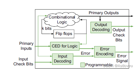
Fig. 1.12 Trojan mitigation at runtime, based on concurrent error detection (CED) and
input/output as well as error encoding modules. The latter are required for the overall system,
where multiple chips of the outlined architecture will be linked together for cross-verification.
Adopted from [Wu+16]
此外,诸如逻辑锁定和拆分制造等IP保护方案,在一定程度上也可以阻止在制造过程中植入木马。这是因为
如果缺乏对设计布局和IP的充分理解,攻击者无法轻易植入特定、有针对性的木马[Ime+13a, Pat+19b]。

Fig. 1.12 基于并发错误检测(CED)与输入/输出以及错误编码模块,在运行时缓解木马攻击。错误编码模块是整系统所必需的,在系统中,所述架构的多个芯片将被链接在一起进行交叉验证,摘自[Wu+16]。
1.1.2.5 Physically Unclonable Functions
When applied some input stimulus, a PUF should provide a fully de-correlated
output response. This response must be reproducible for the very same PUF, even
under varying environmental conditions, but it must differ across different PUF
instances, even for the same PUF design. The desired properties for PUFs are
uniqueness, unclonability, unpredictability, reproducibility, and tamper-resilience.
1.1.2.5 物理不可克隆函数
当施加一些输入激励时,PUF应提供完全去相关的输出响应。即使在不同的环境条件下,针对同一PUF,这种响应必须是可重复的。同时,即使是同一批次的PUF设计,对于不同的PUF实例,响应信号也必须不同。PUF应具备的性质包括唯一性、不可克隆性、不可预知性、可重复性、以及防篡改性。
PUFs are used for (1) “fingerprinting” or authentication of hardware, using
the so-called “weak PUFs” that provide capabilities for processing only one/few
fixed inputs, or (2) challenge-response-based security schemes, using the so-called
“strong PUFs” that provide capabilities for processing a large number of inputs
[Her+14, MV10, CZZ17]. Note that “weak PUFs” are not necessarily inferior to
“strong” PUFs [Rüh+13a]. On the contrary, powerful machine learning attacks such
as [CZZ17, Rüh+13a, Liu+18, Gan17] do not apply for weak PUFs, only for strong
PUFs. The main difference between weak and strong PUFs is that, as indicated, the
former work on a (few) fixed input(s), or inputs or challenge(s), whereas the latter
have to support a large range of challenges. See Fig. 1.13 for the outline of a default,
generic authentication scheme using a strong PUF.
PUF可被用于:(1)采用所谓的“弱 PUF”(仅能处理一个/少数固定输入信号),实现硬件的指纹或认证;
(2)采用所谓的 “强PUF”(具备处理大量输入信号的能力),实现基于"挑战-响应"模式的诸多安全特性[Her+14, MV10, CZZ17]。
值得注意的是,弱PUF并不一定比强PUF脆弱[Rüh+13a]。相反,基于机器学习的强力攻击,例如
[CZZ17, Rüh+13a, Liu+18, Gan17]等都对弱PUF无效,只适用于强PUF。如前所述,弱PUF和强PUF的主要区别在于,前者是在少量的固定输入/挑战上工作,而后者则必须支持大量的挑战。图1.13展示了一个使用强PUF进行认证的缺省的通用方案。
Electronic PUFs represent the dominant class of PUFs, with prominent types
of electronic PUFs using ring oscillators, arbiters, bistable rings, and memories
[MV10, Her+14, Gan17, CZZ17]. Such PUFs are relatively simple to implement
and integrate, even for advanced processing nodes. The core principle for such
PUFs is to leverage the process variations inherent to CMOS fabrication and
operation, through various dedicated circuitry. However, the resulting randomness
is limited for most CMOS PUF implementations; it may be machine-learned and,
thus, cloned [CZZ17, Rüh+13a, Liu+18, Gan17].
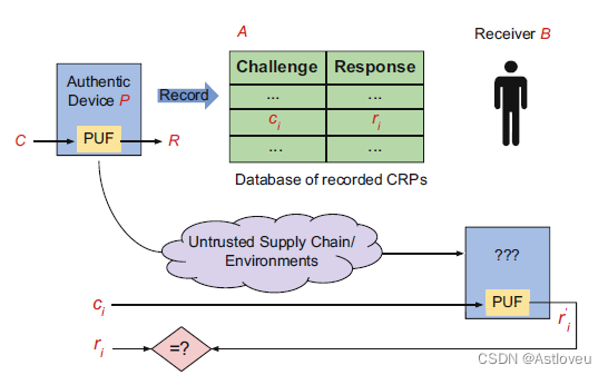
Fig. 1.13 A default, generic authentication scheme using a strong PUF. The trusted entity A
collects a set L of challenge-response pairs (C, R) generated from the PUF P and stores L in
a database for interrogation in the field. P is then delivered to B so that the PUF can be used by
B for authentication with A. To do so, A randomly selects an unseen challenge ci , sends it to B,
who applies it to P to generate the response ri . This response is sent back, whereupon A checks
ri against the corresponding response ri in its database; in case these responses match (subject to
error tolerances as allowed for by the particular protocol), B is successfully authenticated using P.
Adopted from [CZZ17]
电子PUFs代表了PUFs的主流,其主要类型的实现基于环形振荡器、仲裁器、双稳态环和存储器[MV10, Her+14, Gan17, CZZ17]。此类 PUF 的实现和集成相对简单,即使对于依赖先进工艺处理的节点,亦是如此。此类PUF的核心原理是通过各种专用电路来利用CMOS制造与操作中固有的工艺变化。然而,对于大多数CMOS PUF的实现而言,其产生的随机性是有限的,可通过机器学习来破解,并实现克隆[CZZ17, Rüh+13a, Liu+18, Gan17]。

Fig. 1.13 缺省的、使用强PUF的通用认证方案示例,摘自[CZZ17]。受信实体A 存有一组由PUF P生成的挑战-响应对(C,R),称之为集合L,并将L存储在数据库中,以供现场质询。 然后将P交付给B,这样PUF就可以被B用来结合A进行认证。
为此,A 随机选择一个未见过的挑战码 ci,将其发送给 B,B 将其应用于 P 以生成响应码ri。
此响应码再被送回A,并由 A 检查ri是否与其数据库中的对应的响应码匹配;如果匹配(匹配机制受制于特定协议的容错要求),则认为B使用P认证成功。
Optical PUFs represent another interesting class [Pap+02, Rüh+13b, TŠ07,
MV10, Gru+17, Kne+19]. In fact, the very first PUF proposal in the literature,
proposed by Pappu et al. [Pap+02] in 2002, devised an optical token from
transparent epoxy with randomly inserted, micrometer-sized glass spheres. Thus,
the idea of optical PUFs is to manufacture an “optical token” that, in addition
to structural variations inherently present in selected optical media, may contain
randomly included materials, e.g., nanoparticles. Besides such a token, optical
PUFs require further components, for generating the optical input and processing
the output. The fundamental phenomena underlying an optical PUF are scattering,
reflection, coupling, and absorption of light within the optical token. Depending
on the materials used for the token and the inclusions as well as the design
of the token itself, these phenomena can be highly chaotic and nonlinear by
nature [Kne+19, Gru+17]. Hence, optical PUFs are considered more powerful than
electronic PUFs.
另一类有趣的PUF是基于光学的 [Pap+02, Rüh+13b, TŠ07,
MV10, Gru+17, Kne+19]。事实上,文献中第一个 PUF 提案是由 Pappu 等人于2002年提出的[Pap+02] ;在该方案中,作者设计了一个由透明环氧树脂制成的光学标记,其中随机插入了的微米级的球状玻璃。 因此,光学PUF的理念是制造一个基于光学的特定标记,其中除了具有所选光学介质中固有的结构变化之外,还可包含诸如纳米粒子等随机材料。除了这样的标记,光学PUF还需要更多的组件,用于生成输入光学信号和处理输出光学信号。光学 PUF 的基本现象是光线在光学标记内的散射、反射、耦合与吸收。这些现象本质上是高度混乱和非线性的,具体取决于标记与内含物所用的材料以及标记本身的设计 [Kne+19, Gru+17]。因此,通常光学 PUF被认为强于电子 PUF。
1.2 Limitations of CMOS Technology for Hardware Security
Most of the hardware security primitives we have visited in the previous sections
have been predominantly CMOS-centric. However, emerging devices bring a new
facet to this equation, by offering unique properties that can reshape the way we
think about hardware security. This confluence of hardware security and emerging
devices has been gaining traction over the recent years owing to new physics and
materials research, which has resulted in the development of novel logic and memory
devices. In this section, we first discuss the limitations of CMOS technology for
hardware security, which have driven this push toward emerging technology-based
solutions, before delving into the specific characteristics of emerging technologies
that make them promising for upcoming security primitives:
1.2 CMOS技术在硬件安全方面的局限性
本文前几节中所介绍的的大多数硬件安全基元,在主体上均以CMOS为中心的。 然而,新兴的元器件打破了这种单一的局面,通过提供独特的技术属性,重塑了我们对硬件安全的思考方式。近年来,得益于物理学和材料科学的最新研究进展,使硬件安全和新兴元器件的结合获得了助力,推动了新型逻辑和存储器件的发展。 未来具有前景的安全基元都会基于这些新兴技术。在本节中,在深入探讨新兴技术的先进特性之前,我们将首先讨论CMOS技术在硬件安全方面的局限性,因为正是这些局限,才构成了新兴技术演进的动力:
- In general, emerging technologies seek to overcome the fundamental CMOS
limitations regarding power consumption, among other aspects. Power overheads
are a crucial consideration while securing any CMOS IP, with full-chip protection
often requiring a large sacrifice in terms of constraining the power budget. This
typically prohibits the percentage of the chip that we can feasibly secure. On
the other hand, many emerging devices have been shown to exhibit ultra-low
operating power, thus enabling the designer to secure a larger portion of the chip
without exacerbating power consumption.
总的来说,新兴技术寻求克服CMOS在功耗等方面的限制。在保护任何 CMOS IP 时,功率开销是一个重要的考虑因素,全芯片级别的保护通常需要在限制功率预算方面做出巨大牺牲。这通常限制了保护芯片IP的可行性。 另一方面,许多新兴的器件已被证明具有超低的运行功耗,从而使设计人员能够实现更大部分芯片IP的保护,而不加剧功耗。
- Similarly, the scalability of CMOS-based security primitives has been a cause for
concern, since they can often result in blowing up the chip area, thus increasing
the fabrication costs. In contrast, emerging devices cannot only possess a smaller
device footprint, but in most cases also allow the designer to implement logic
more efficiently, thus saving valuable die area.
同样,基于CMOS的安全基元的可扩展性也令人担忧。因为它们通常会导致芯片面积的膨胀,从而增加了 制造成本。
相比之下,新兴器件不仅拥有更小的尺寸,而且在通常情况下还使得设计人员能够更有效地实现功能逻辑,从而节省宝贵的芯片面积。
- The existing CMOS framework has always been built with the primary intent of
improving the performance and efficiency of modern electronics, with security
being retrofitted as an afterthought. Emerging devices afford us the opportunity
to embed security as a primary design metric in the supply chain and allow a
security-focused device-circuit co-design process.
现有的CMOS框架创建一直是以提高现代电子产品的性能和效率为主要目的,而安全性则被作为事后才需要考虑的问题。
新兴设器件为我们提供了机会,使安全性可成为供应链中的主要设计指标,并使得元器件的电路设计成为以安全为中心的协同设计过程。
- Conventional CMOS logic styles and synthesis techniques are well documented
and have been around for a long time. These do not offer much flexibility in terms
of patching circuit- and system-level security vulnerabilities. However, emerging
devices can potentially allow completely new logic design styles to counter those
vulnerabilities, owing to their unique construction and operation. For instance,
novel ferroelectric and spintronic logic devices with non-volatility can enable
memory-in-logic, thus opening the doors to new non-von Neumann computing
paradigms.
传统的 CMOS 逻辑样式和综合技术都是有据可查的,且在业界有着较长的应用历史。但是,对于电路级和系统级的安全漏洞的修补,它们并没有提供太多的灵活性。然而,得益于新兴器件独特的结构和操作功能,它们可提供全新的逻辑样式来应对这些安全漏洞。例如,具有非易失性的新型铁电和自旋电子逻辑器件可以实现逻辑记忆(memory-in-logic),从而开启了通往新型"非冯.诺依曼计算范式"的大门。
It must be noted that although these emerging technologies appear promising
and practical for the near future, they will likely be built to augment the existing
CMOS framework, not supplant or replace it. In this context hybrid CMOS-emerging
electronics such as the N3XT architecture [Aly+18], which combine carbon nanotubes
and spintronics within CMOS 3D ICs, might not be a distant reality.
必须指出的是,尽管这些新兴技术颇具前景,在不久的未来就会投入实用,但它们很可能是为了增强现有的 CMOS框架,而不是取而代之。在此情况下,混合新兴CMOS电子器件( hybrid CMOS-emerging electronics),如N3XT架构[Aly+18] (它将碳纳米管和自旋电子结合在CMOS 3D集成电路中),可能在不远的将来就会实现。
1.3 Inherent Properties of Emerging Technologies to
Advance Hardware Security
As mentioned in Sect. 1.2, various emerging technologies offer the potential to
advance the notion of hardware security. Figure 1.14 outlines selected emerging
technologies, their properties relevant and beneficial for hardware security, the
security schemes that are supported accordingly, and the security threats countered
by such schemes.
1.3 促进硬件安全的新兴技术内在特性
正如在第1.2节中提到的,各种新兴技术都提供了推进硬件安全概念的潜力。
图 1.14 概括了所选的新兴技术,包括它们裨益于硬件安全的相关特性、特性所支持的安全方案,以及这些方案
所应对的安全威胁。
The emerging devices included in Fig. 1.14 have some interesting properties in
common, which are more difficult to achieve in traditional CMOS technology.More
specifically, spintronic devices, memristors, carbon nanotube field effect transistors
(CNTFETs), and Silicon Nanowire field effect transistors (SiNWFETs) can all be
tailored to achieve significant variability/randomness, reconfigurability or polymorphic
behavior, resilience against reverse engineering, heterogeneous integration,
and also the possibility of separating trusted and untrusted parts. Therefore, these
devices can serve well for PUFs, TRNGs, IP protection schemes, and to mask sidechannel
leakage. Moreover, memristors may also offer resilience against tampering,
by means of destructive data management. It should be understood that the prospects
for actual implementation of such security schemes based on emerging devices
depend on various aspects, ranging from circuit design and security analysis in
general, down to manufacturing capabilities and device maturity, among others.
Next, we briefly discuss some of these unique properties of emerging devices, which
make them prime candidates for the next era of secure electronics.
图 1.14 所列新兴器件具有一些有趣的、且很难通过传统 CMOS 技术实现的特性。
具体而言,自旋电子器件、忆阻器、碳纳米管场效应管(CNTFETs)以及纳米线场效应管(SiNWFETs)都可以通过定制来实现显著的可变性/随机性、可重构性或多态性行为、抗逆向工程的防护韧性、异构集成,以及拆分可信与非可信部分的能力。
还有可能将可信和不可信的部分分开。因此,这些器件可以很好地用于PUFs、TRNGs、IP保护方案以及掩盖侧信道泄漏信号。
此外,忆阻器还可以通过对数据的破坏性管理,来提供对篡改攻击的防护韧性。
应该了解的是,此类基于新兴器件的安全方案的实际应用前景取决于多方面因素,一般来说,从电路设计和安全分析,直至制造能力和器件成熟度等等。接下来,我们将简要讨论新兴器件的部分独特性质,正是这些特性使其成为新一代电子安全的首选。
1.3.1 Reconfigurability
Reconfigurability, in the context of emerging devices, refers to the ability of a single
device topology to be configured for different logic functionalities, depending on
external control signals or internal parameters like doping, etc. Essentially, it means
that the same device layout could possibly implement one of several logic gates,
each indistinguishable from each other. However, once configured and deployed
in the field, the reconfigurable device will retain its functionality. Yet, the very
fact that the particular functionality it implements could be one of many, increases
the computational complexity for an attacker seeking to decipher its true nature.
This is particularly useful for static camouflaging schemes, where the number of
functionalities that the emerging logic gate can implement decides the number of
key bits per camouflaged gate. Here, the multi-functional gate could be configured
for its intended logic, post-fabrication, in a secure facility. Some classes of devices
that exhibit reconfigurability include the giant spin Hall effect device [Ran+19],
SiNWFETs [Rai+18], and memristors [Xia+09].
1.3.1 可重构性
在新兴器件的背景下,可重构性是指单一器件拓扑结构可根据不同的逻辑功能被重新配置的能力,
这取决于外部控制信号或内部参数,如掺杂程度(doping)等。本质上,这意味着相同的器件布局可能
实现多个逻辑门之一的功能,而每个逻辑门都无法与彼此区分开。而一旦可重构器件完成了重构并在现场部署完毕,它将一直保留特定的功能。然而,关键事实是,该特定功能只是它能实现的众多功能之一,对于寻求破解其真实性质的攻击者而言,这极大增加了计算复杂度。这一点对静态伪装方案特别有用,因为在静态伪装方案中,新兴器件(多功能门)可实现的功能数量决定了每个伪装门的关键比特位数。在这里,在完成制造后,可以在安全设施中将多功能门配置为支持预期逻辑。一些支持可重构性的器件类别包括巨型自旋霍尔效应器件 [Ran+19]、硅纳米线场效应管 [Rai+18] 和忆阻器 [Xia+09]。
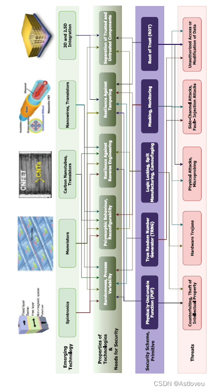
Fig. 1.14 A selective overview on emerging technologies, their properties, matching security schemes, and countered threats
Fig. 1.14 对新兴技术及其特性、对应的安全方案、威胁应对的选择性概述
1.3.2 Runtime Polymorphism
The ability to undergo reconfiguration in the field is referred to as runtime
polymorphism in this monograph. Runtime polymorphic emerging devices cannot
only be programmed for functionality once post-fabrication, but can be morphed any
number of times on-the-fly. This characteristic makes them useful for implementing
polymorphic logic for hardware security. The difference between reconfigurable and
polymorphic logic from the context of the attacker is that while reconfigurable gates
present the attacker with the conundrum of correctly identifying the true nature of
the logic from many possible functionalities, polymorphic logic actually morphs
between those various possible functional states in real-time. Thus, an attacker
seeking to RE the polymorphic circuit not only has to identify these functional
states but also the transformation scheme between the states. Polymorphic emerging
devices proposed in prior works include the magnetoelectric spin–orbit device
(MESO) [Man+19] and magnetic domain wall (DW)-based devices [Par+17].
1.3.2 运行时多态性
在本文中,将"在现场进行功能重构的能力"称为运行时多态性。支持运行时多态性的新兴器件
不仅可以在制造完成后进行一次功能编程,还可以随时随地调整变化。此特性使其可用于实现
硬件安全的多态逻辑。从攻击者的角度来看,可重构逻辑和多态逻辑的区别在于,可重构门
给攻击者的难题是如何从许多可能的功能项中正确识别系统真实的性质,而多态逻辑实际上是在这些可能的
功能状态之间实时变迁。因此,对于寻求逆向破解多态电路的攻击者而言,不仅要识别这些功能状态,还要识别状态间的转移方案。在之前的工作中提出的多态性的新兴器件包括磁电自旋轨道器件(MESO) [Man+19] 和基于磁畴壁的器件[Par+17]。
1.3.3 Nonlinearity and Intrinsic Entropy
Nonlinearity in an emerging device refers to its ability to perform nonlinear
transformation operations on the input stimulus, wherein the input to output
mapping becomes nonlinear or deviates from direct proportionality. Such an
injective one-way nonlinear transformation is quite useful for generating keys in
a physical unclonable function setting. Examples of nonlinear emerging devices
finding applications in cryptographic key generation include memristors [Zha+18b]
and photonic micro-cavity-based devices [Gru+17].
Intrinsic entropy of an emerging device is the innate randomness in the physical
phenomenon driving the device. Such randomness could arise due to any number
of factors such as metastability or abruptness in switching processes, or chaotic
dynamics. Evidence of intrinsic entropy has been observed in several emerging
devices such as spintronics switches [Ven+15] and photonic systems [SR07].
1.3.3 非线性和内在熵
新兴器件中的非线性是指其对输入激励信号进行非线性转换的能力。其中输入与输出的映射关系为非线性或偏离直接的等比例关系。这种单向非线性变换可用于在物理不可克隆函数设置中生成密钥。用于加密密钥生成的非线性新兴器件类别包括忆阻器[Zha+18b]和基于光子微腔的器件[Gru+17]。
新兴器件的内在熵指的是驱动器件的物理学现象的内在随机性。这种随机性可能是由于多种因素引起的,例如状态切换过程中的亚稳态或突发性,或混沌动力学特性。内在熵的证据已经在几种新兴器件中观察得到,例如自旋电子开关 [Ven+15] 和光子系统 [SR07] 等。
1.3.4 Heterogeneous Physical Integration
Emerging technologies like 3D and 2.5D integration allow for the bifurcation of
the chip into security-critical and non-critical components, thus enabling schemes
like split manufacturing to come into the picture. The possibility of physical
separation and integration of the chip in the supply chain enables the designer
to incorporate safeguards against IP theft and insertion of malicious Trojans.
Besides, the heterogeneous integration of novel emerging devices into hybrid-
CMOS configurations within the 3D framework opens up opportunities to tap
the unique characteristics of those devices, for e.g., in-memory computing in 3D
architecture [Aly+18].
1.3.4 异构物理集成
3D与2.5D集成等新兴技术,允许将芯片分为安全攸关和非安全攸关组件部分,从而使拆分制造等方案成为可能。
在供应链中,通过对芯片进行物理拆分和集成,使得设计人员可以采纳入保护措施,以对抗知识产权盗窃和木马的恶意植入。
除此之外,在3D框架内将新兴器件异构集成至混合CMOS的配置中,也为开发利用这些器件的独特性质提供了机会,例如,实现3D架构中的内存计算[Aly+18]。
1.3.5 Resilience Against Tampering and Side-Channel Attacks
Tamper- and side-channel resilience in an emerging device or technology arises
from the ability to shield its internal operation and switching activity from an outsider.
This could be achieved via a number of techniques like materials engineering
to make the device impervious to external stimuli from probes, or constructing
physical barriers to obstruct an attacker from accessing internal nodes and
wires. Immunity against side-channel attacks also stems from features that aid
in securing the leakage channels, like masking or modifying the power activity
visible to the attacker. For instance, triple-independent gate field effect transistors
(TIGFET) [Sha+20] and all-spin logic [AYL18] have been shown to be resistant
to power side-channel attacks due to symmetric I-V and symmetric read/write
characteristics, respectively.
1.3.4 抵御篡改与侧信道攻击的韧性
新兴器件和技术对于篡改和侧信道攻击的防御韧性,源自于它保护内其部操作和开关活动不受外界影响的能力。
这可以通过材料工程等多种技术来实现,使器件不受来自探测器的外部刺激的影响,或构建阻止攻击者访问内部节点和
线路的物理屏障。对侧信道攻击的免疫能力也源于有助于保护泄露信道的特性,例如屏蔽或修改功率相关的活动,使之对
攻击者不可见。例如,三重独立门场效应管(TIGFET)[Sha+20]和全自旋逻辑[AYL18]得益于对称的I-V和读/写特性,已被证明对功率侧通道攻击有一定的抵抗能力。
1.4 Closing Remarks
Our future electronics and computing systems can be fortified against various
classes of hardware threats by looking beyond conventional CMOS design practices,
toward the vast array of emerging logic and memory technologies. Some of these
emerging devices have shown promise in mitigating the common hardware-based
concerns known to plague CMOS systems, owing to their unique and peculiar
properties. In this chapter, we first looked at the fundamentals of hardware security,
including the various threat scenarios and attack landscapes against modern computing
systems, and the plethora of solutions proposed to counter them. Then we tried to
understand the limitations of CMOS hardware with respect to securing hardware, at
the root level, and also delved into the specific properties of emerging technologies
that can address these limitations. These properties, viz. reconfigurability, runtime
polymorphism, nonlinearity, intrinsic entropy, heterogeneous physical integration,
tamper-resilience, and resistance against side-channel leakage, form the basis of
individual security primitives that will be discussed in the upcoming chapters.
1.4 结束语
针对未来的电子和计算系统,我们可以通过超越传统的CMOS设计实践,并将目光投向大量的新兴逻辑和存储技术,
来加强对各类硬件威胁的防范。其中一些新兴的器件已经展示出了独特的性质,有望减轻困扰CMOS系统的常见安全问题。
在本章中,我们首先探讨了硬件安全的基本原理,包括针对现代计算系统的各种威胁和攻击概况,以及为应对这些威胁而提出的大量解决方案。 然后,我们试图从根源上理解CMOS在保护硬件安全方面的局限性,并深入研究了可以克服这些限制的
一系列新兴技术特性。 这些特性,包括可重构性、运行时多态性、非线性、内在熵、异构物理集成、抗篡改性以及抗侧信道泄露,逐一构成了基本的安全基元。我们将在接下来的章节中分别讨论这些安全基元。
五
级
标题


 387
387


 被折叠的 条评论
为什么被折叠?
被折叠的 条评论
为什么被折叠?
 到【灌水乐园】发言


