


目录
1. Armv9 Cortex CPU
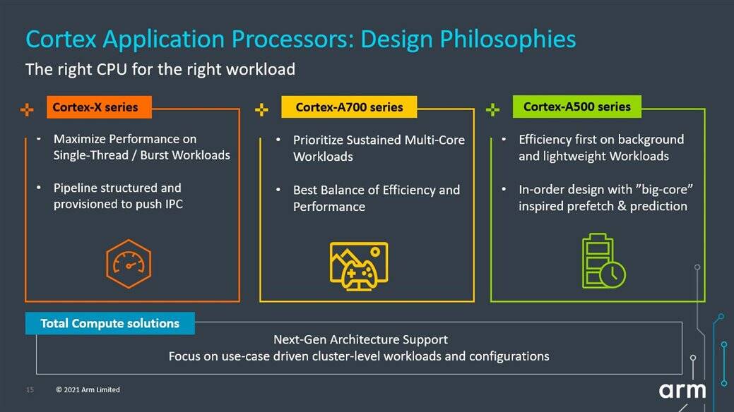
Cortex-X 系列旨在最大限度地提高单线程和“突发”工作负载的性能,微架构中的 pipeline 经过结构化和配置以推动 IPC 性能改进。
Cortex-A700 系列优先用于持续多处理器工作负载,为需要在热约束范围内保持持续性能的工作负载提供效率和性能的最佳平衡。
Cortex-A500 系列专注于轻量级工作负载,并以效率为先的设计重点。这些“小”核心的部分灵感来自我们之前的一些更大的核心,现在采用预取(pre-fetch)和预测(predication)作为关键的微架构特性。
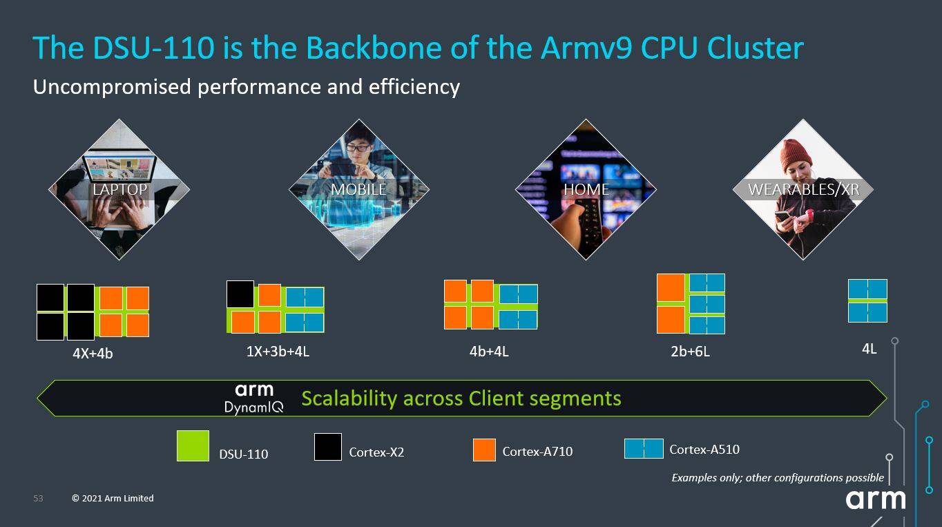
MediaTek Dimensity 9000 是一款基于 ARMV9 技术的 SOC,采用 1+3+4 big.LITTLE 技术:
- Cortex-X2(1 core) : 极致性能
- Cortex-A710(3 core): 最佳性能/功率平衡
- Cortex-A510(4 core): 最佳电源效率
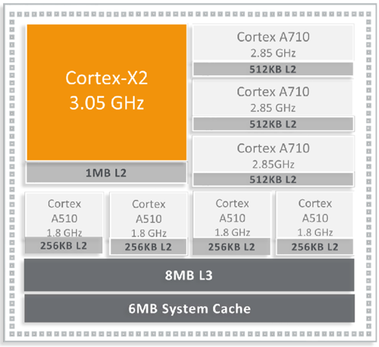
big.LITTLE 是一种兼顾电源效率(Power Efficiency)和性能(Performance)的处理器异构处理架构,使用两种类型的处理器:
- LITTLE 处理器旨在实现最大功率效率,比如:Cortex-A510
- big 处理器旨在提供最大计算性能,比如:Cortex-X2, Cortex-A710
big.LITTLE 解决方案能够适应智能手机、平板电脑和其他设备的动态使用模式。Big.LITTLE 适应在复杂的应用程序中,高处理强度的任务(如手机游戏和网页浏览)与通常较长时间的低处理强度任务(如短信、电子邮件和音频)交替进行。Cortex-X2 和 Cortex-A710 处理器的性能能力可用于繁重的工作负载,而 Cortex-A510 则可以接管大多数智能手机工作负载并高能效地处理,其中包括操作系统活动、用户界面和其他始终在线、始终连接的任务。
2. Key Features
| Cortex‑X2 | Cortex‑A710 | Cortex‑A510 |
|---|---|---|
|
|
|
- Cortex‑X2 和 Cortex‑A710 关键功能基本相同,而 A510 则精简很多
- 只有中核 A710 支持 A32 指令架构
- A510 不支持乱序流水线
3. Cortex®‑X2
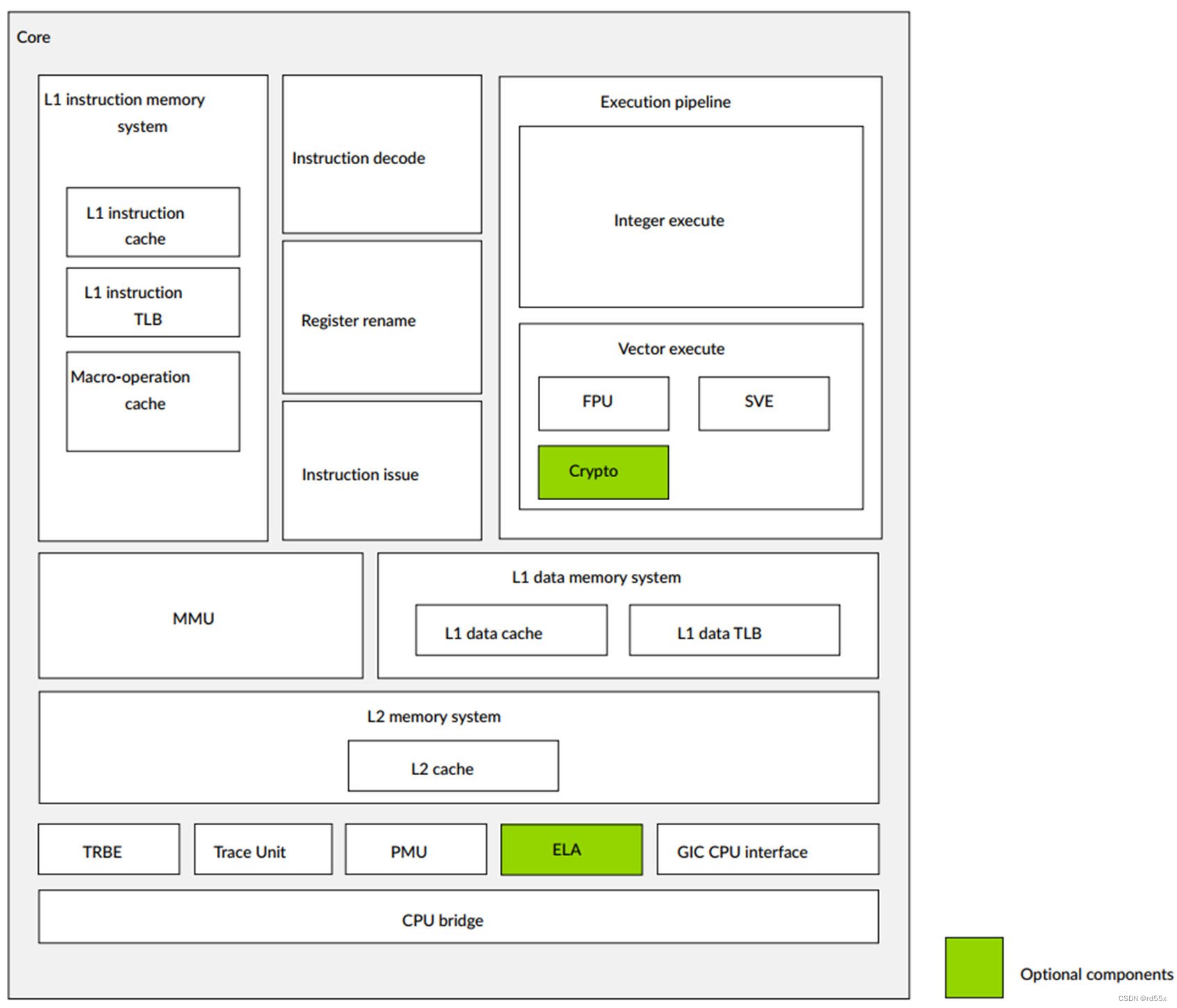
3.1 Core Components
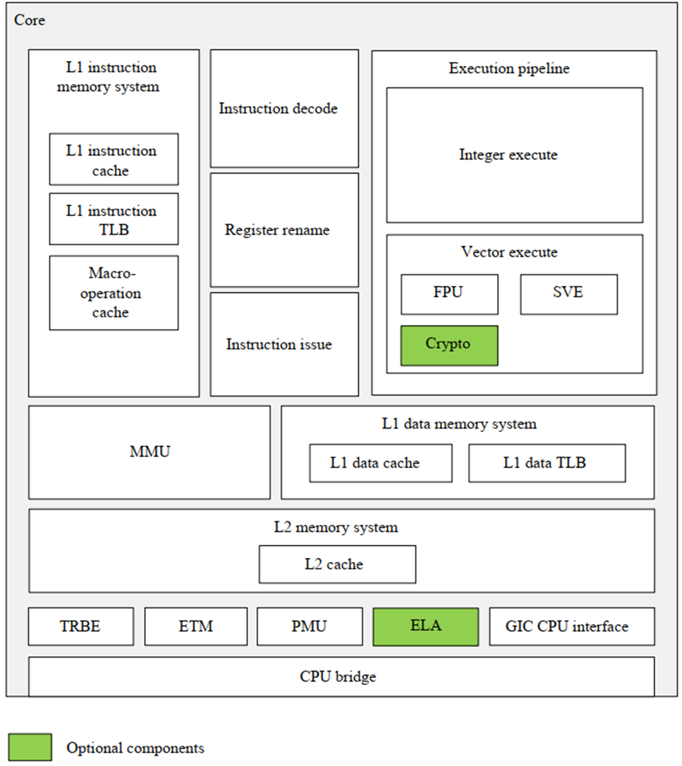
L1 Memory System
哈佛架构,指令 cache 和数据 cache 分离,包括 L1 Instruction Memory System 和 L1 Data Memory System 。
L1 Instruction Memory System
从指令缓存中取出指令并将指令流传递给指令解码单元,包括:
- L1 instruction cache
- 64KB
- 4-way set associative
- 64-byte cache lines
- L1 instruction Translation Lookaside Buffer (TLB)
- fully associative
- native support for 4KB, 16KB, 64KB, and 2MB page sizes
- Macro-operation (MOP) cache
- 3072-entry
- 4-way skewed associative L0 Macro-OP (MOP) cache:其中包含已经解码和优化的指令以获得更高的性能
- dynamic branch predictor(动态分支预测器)
L1 Data Memory System
用于执行加载和存储指令。包括:
- L1 data cache
- 64KB
- 4-way set associative
- 64-byte cache lines
- L1 data Translation Lookaside Buffer (TLB)
- fully associative
- native support for 4KB, 16KB and 64KB page sizes and 2MB and 512MB block sizes
Instruction Decode
指令译码单元,将 Arch64 指令译码成为内部格式。
Register Rename
寄存器重命名单元,执行寄存器重命名以促进乱序执行并将解码的指令分派到不同的发射队列。
Instruction Issue
指令发射单元,控制何时将解码的指令分派到执行流水线。它包括发射队列,用于存储待分配到执行流水线的指令。
Execution Pipeline
Execution Pipeline 时执行指令的流水线,由 Integer Execute 和 Vector Execute 两部分组成:
Integer Execute
整数计算执行流水线,包括执行算术和逻辑数据处理操作的整数执行单元。
Vector Execute
向量计算执行单元,执行高级 Single Instruction Multiple Data (SIMD) 和浮点运算 (FPU) 操作,包括:
- Scalable Vector Extension (SVE) 指令
- Scalable Vector Extension 2 (SVE2) 指令
- 可以选择是否支持执行加密(Crypto)指令
高级 SIMD 是一种媒体和信号处理架构,主要为音频、视频、3D 图形、图像和语音处理添加指令。
浮点运算架构提供对单精度和双精度浮点运算的支持。
Memory Management Unit
内存管理单元 (MMU) 通过存储在转换表(TLB )中的一组虚拟到物理地址映射和内存属性来提供细粒度的内存系统控制。当地址被转换时,它们被保存到 TLB 中,TLB 条目还包括:
- 全局和地址空间标识符(Address Space IDentifiers,ASID):以防止上下文切换导致 TLB 失效。
- 虚拟机标识符(Virtual Machine IDentifiers,VMID):以防止虚拟机管理程序(hypervisor)切换虚拟机时导致 TLB 失效。
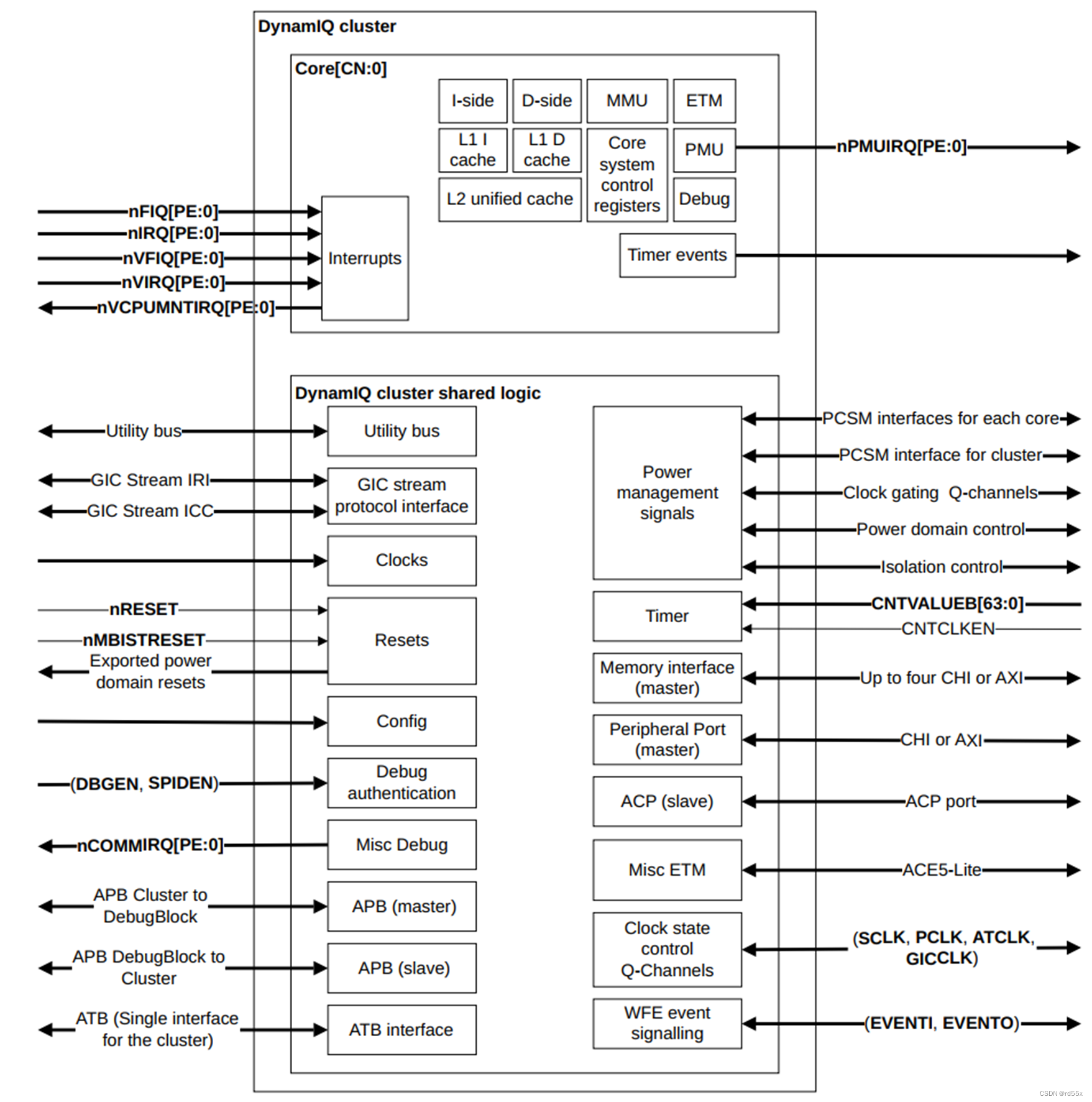
L2 Memory System
通过 CPU 桥将内核与 DynamIQ Shared Unit-110 (DSU-110) 连接起来。它包括 :
- L2 cache
- 512KB or 1MB
- 8-way set associative, 4 banks
- L2 Translation Lookaside Buffer (TLB)
L2 缓存对集群中的每个 Cortex‑X2 Core 都是统一的(unified)和私有的(private)。
CPU Bridge
在一个集群中,每个 Cortex®‑X2 内核和 DSU-110 之间都有一个 CPU 桥接器,CPU 桥控制 Core 和 DSU-110 之间的缓冲和同步。
CPU 桥是异步的,以允许每个 Core 有不同的频率、功率和面积实现。可以将 CPU 桥配置为同步运行,而不会影响始终异步的其他接口,例如调试和跟踪。
GIC CPU interface
Generic Interrupt Controller CPU 接口,与外部分发器组件集成,是一种在集群系统中用于支持和管理中断的资源。
3.2 Core Pipeline
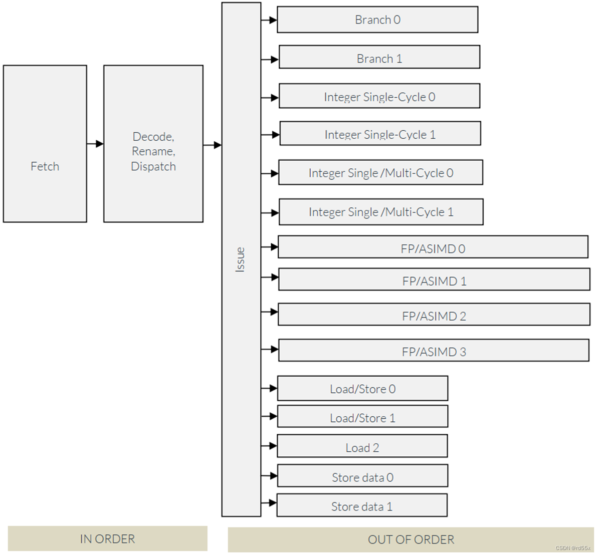
Cortex-X2 执行指令的步骤:
- 从 L1 指令缓存中获取指令
- 将指令解码为 Macro-OPerations (MOPs)
- 寄存器重命名(Register renaming)和发送(dispatch )阶段:一个 MOP 拆分为两个 MicroOPerations (µOPs)
-
µOP 等待其操作数并无序地向 15 个 issue pipelines 之一发送(每个 issue pipeline 每个周期可以接受一个 µOP)
Execution Pipelines 支持不同类型的操作,如下表所示。
| Instruction groups | Instruction |
|---|---|
| Branch 0/1 | Branch µOPs |
| Integer Single-Cycle 0/1 | Integer ALU µOPs |
| Integer Single/Multi cycle 0/1 | Integer shift-ALU, multiply, divide, CRC and sum-of-absolute-differences µOPs |
| Load/Store 0/1 | Load, Store address generation and special memory µOPs |
| Load 2 | Load µOPs |
| Store data 0/1 | Store data µOPs |
| FP/ASIMD-0 | ASIMD ALU, ASIMD misc, ASIMD integer multiply, FP convert, FP misc, FP add, FP multiply, FP divide, FP sqrt, crypto µOPs, store data µOPs |
| FP/ASIMD-1 | ASIMD ALU, ASIMD misc, FP misc, FP add, FP multiply, ASIMD shift µOPs, store data µOPs, crypto µOPs. |
| FP/ASIMD-2 | ASIMD ALU, ASIMD misc, ASIMD integer multiply, FP convert, FP misc, FP add, FP multiply, FP divide, FP sqrt, crypto µOPs. |
| FP/ASIMD-3 | ASIMD ALU, ASIMD misc, FP misc, FP add, FP multiply, ASIMD shift µOPs, crypto µOPs |
4. Cortex®‑A710
4.1 Core Components
Cortex®‑A710 与 Cortex®‑X2 的组成很类似。
4.2 Core Pipeline
Cortex®‑A710 与 Cortex®‑X2 的 pipeline 类似。
5. Cortex®‑A510
5.1 Core Components
A510 设计特点:为高效(high-efficiency)、低功耗(lowpower)和节省面积(area-efficient)
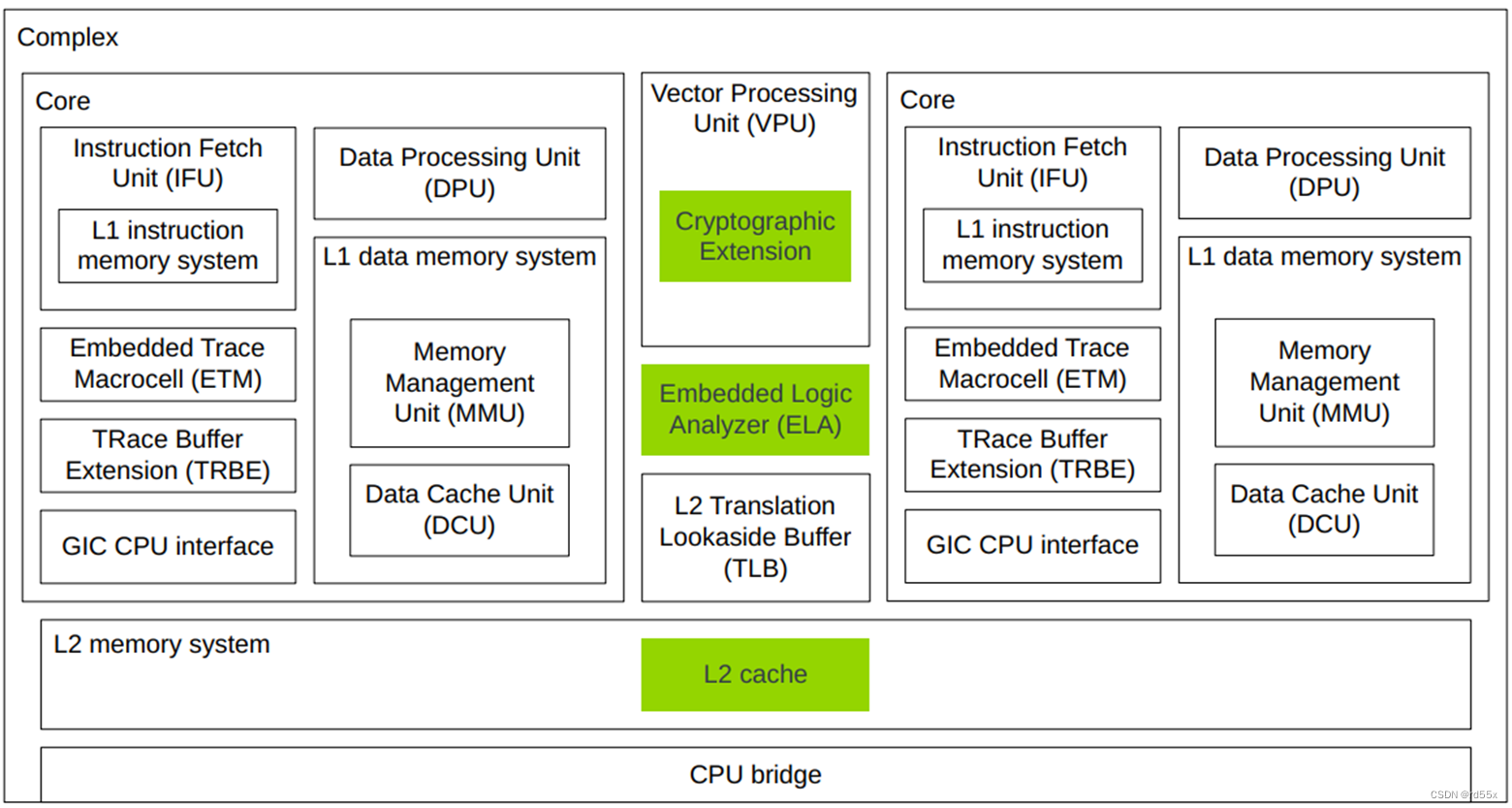
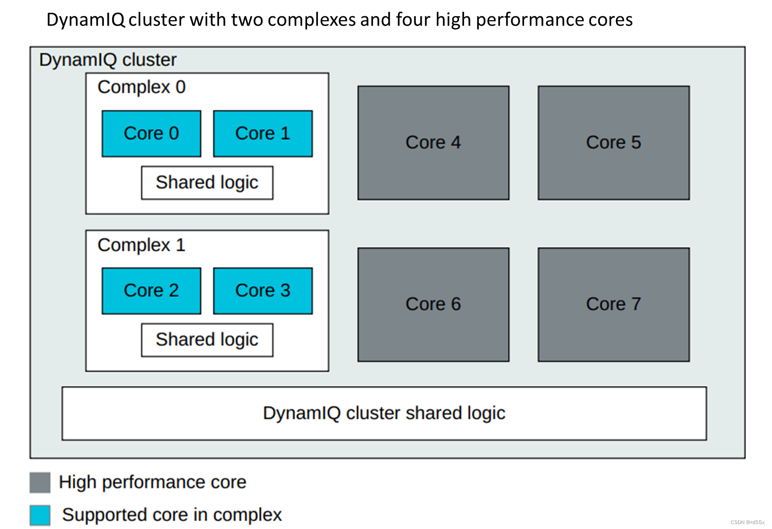
Cortex®‑A510 与 Cortex®‑X2 和 Cortex®‑A710 相比,组成明显的不同。可以被设计成两个 cortex‑a510 core 组成的 complex 或者单个 cortex‑a510 core 的 complex。
Complex
一种可以用于2个 cortex‑a510 core 之间共享部分逻辑单元的设计 ,可共享单元包括:
- L2 cache
- L2 Translation Lookaside Buffer (TLB)
- Vector Processing Unit (VPU)
Instruction Fetch Unit
IFU 从指令缓存或外部存储中获取指令,并使用动态分支预测器来预测指令流中分支的结果。它将指令传递给 DPU 进行处理。IFU 还包括 L1 Instruction Memory System。
L1 Instruction Memory System
它从指令高速缓存中取出指令并将指令流传送到指令解码单元,它包括:
- L1 instruction cache
- 32KB or 64KB
- 4-way set associative
- 64-byte cache lines
- A fully associative L1 instruction TLB
Data Processing Unit
DPU 解码并执行指令,指令被执行时,通过与 DCU 连接的接口从内存系统读取或者写入数据。
DPU 包括性能监控单元 (PMU) 和活动监控单元 (AMU)。
L1 Data Memory System
L1 数据内存系统执行加载和存储指令并服务内存一致性请求,它包括:
- MMU
- fully associative L1 data TLB
- L1 data cache :
- 32KB or 64KB
- 4-way set associative
- 64-byte cache lines
- DCU(Data Cache Unit),用于处理:
- load/store operations
- system register access operations
- A Bus Interface Unit (BIU) that handles the linefills to the L1 data cache
- A STore Buffer (STB) that handles store instructions, cache and TLB maintenance operations, and barriers
GIC CPU interface
Generic Interrupt Controller CPU 接口
Vector Processing Unit
dual-core complex 内的 core 之间共享一个 VPU 。VPU 的功能与 Cortex®‑X2 的 Vector Execute 单元类似。
L2 TLB
dual-core complex 内的 core 之间共享一个 L2 TLB。
L2 Memory System
L2 内存系统可以被 dual-core complex 内的 core 共享。
Cortex‑A510 L2 内存系统将 Cortex®‑A510 内核连接到 DynamIQ™ Shared Unit-110 (DSU-110) L3 内存系统。它包括一个可选的 unified L2 cache,该高速缓存对 complex 来说是私有的。 L2 内存系统处理来自 L1 指令和数据缓存的请求,以及来自 L3 内存系统的 snoop 请求。 L2 内存系统将响应从 L3 系统转发到 core。然后 core 可以根据事务的类型进行精确或不精确的中止。
对于具有两个内核的 complex ,L2 内存系统在两个 core 之间共享。 L2 内存系统还:
- 处理来自 core 和相关L1 evictions (驱逐)的一致(coherent)和非一致(non-coherent)操作。
- 根据 AMBA® 5 CHI 架构规范,处理来自 DSU-110 DynamIQ™ 集群中其他 core 和系统中其他处理元件 (PE) 的 snoop(窥探)操作。
- 将 instruction cache、TLB 和 predictor 维护操作作为分布式虚拟内存 (DVM) 消息处理,包括complex 内的广播操作。
L2 cache
L2 Memory System 它包一个可选的 L2 cache:
- 128KB, 192KB, 256KB, 384KB or 512KB
- 8-way set associative
L2 内存系统通过 CPU 桥接器连接到 DSU-110。
L2 cache 可以配置为具有一个或两个 cache slices。每个 slice 由以下单元组成:
- L2 tag 和数据 RAM
- L2 replacement RAM
- L1 duplicate tag RAM
- 以及相关逻辑
如果存在两个 slices,则根据地址 bit[6] 的值,most traffic from the cores, the L2 TLB, and from downstream snoops is striped across the slices。这种 striping 增加了整体吞吐量。对 Device non-reorderable memory 和 Distributed Virtual Memory (DVM) 的操作访问始终由 slice 0 处理。
每个 L2 cache slice 中的 data RAM 可以配置为单个分区或两个分区。拥有两个分区的RAM,通过允许对不同的 L2 ways 并发访问来增加 L2 缓存读取和写入的峰值吞吐量。
5.2 Core Pipeline
具有直接(direct )和间接(indirect )分支预测的 有序(In-order)流水线。
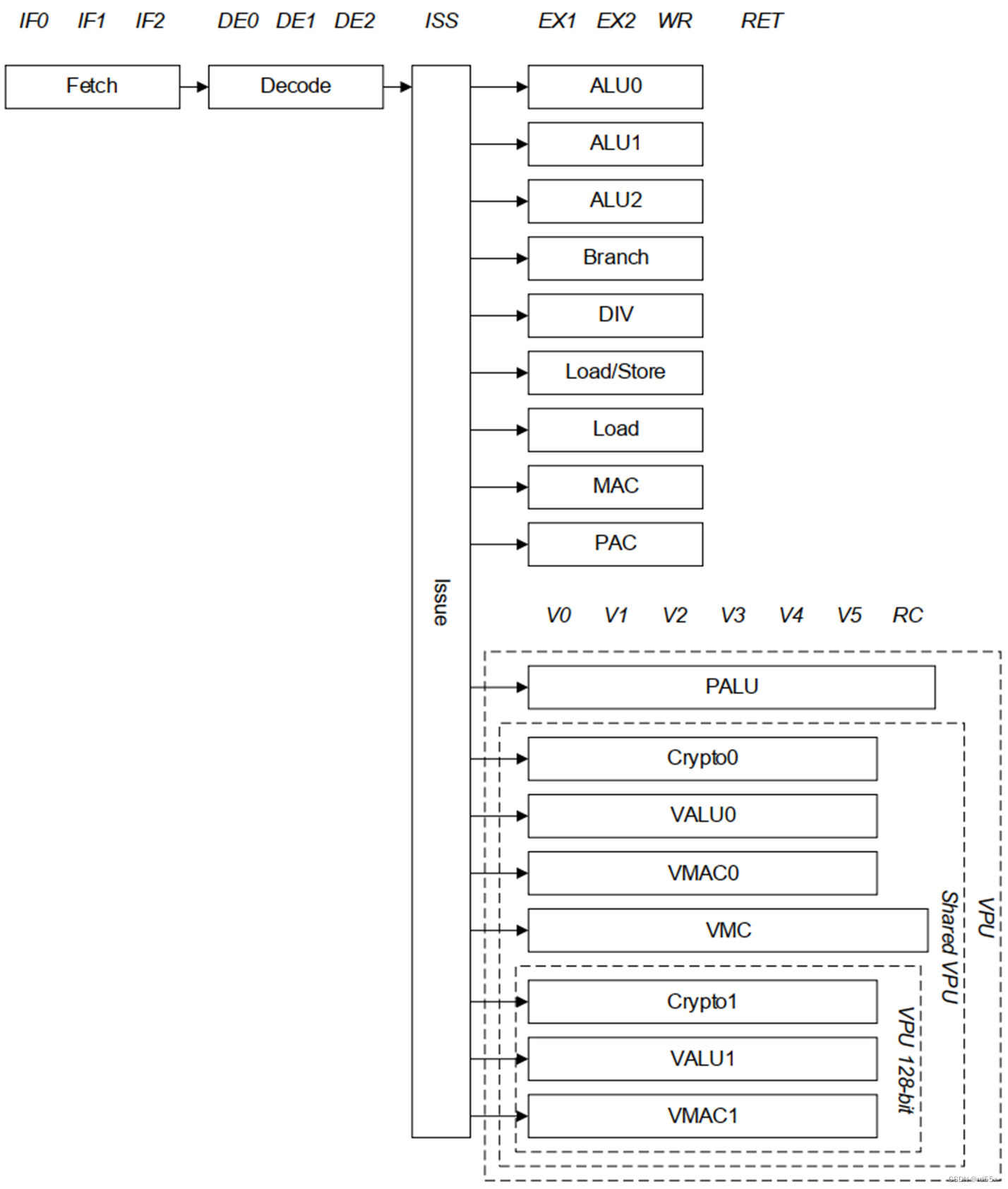
| Pipeline | Instructions |
|---|---|
| ALU0, ALU1, ALU2 | Arithmetic and logic |
| Branch | Branch |
| Crypto0 | Cryptography Supports 1x128-bit operation. This pipeline is shared for dual core configuration. Present only for implementations configured with Cryptographic extensions enabled. |
| Crypto1 | Cryptography Supports 1x128-bit operation. This pipeline is shared for dual core configuration. Present only for implementations configured with Cryptographic extensions enabled and a Vector datapath size of 2x128-bit. |
| DIV | Integer scalar division (iterative) |
| Load/Store | Load and store |
| Load | Load |
| MAC | Multiply accumulate |
| PAC | Pointer Authentication |
| PALU | Predicate register arithmetic and logic |
| VALU0 | Addition, logic and shift for ASIMD, FP, Neon, and SVE Supports 2x64-bit or 1x128-bit operations. This pipeline is shared for dual core configuration. |
| VALU1 | Addition, logic and shift for ASIMD, FP, Neon, and SVE Supports 2x64-bit or 1x128-bit operations. This pipeline is shared for dual core configuration. Present only for implementations configured with a Vector datapath size of 2x128-bit |
| VMAC0 | Multiply accumulate for ASIMD, FP, Neon, and SVE Supports 2x64-bit or 1x128-bit operations. This pipeline is shared for dual core configurations |
| VMAC1 | Multiply accumulate for ASIMD, FP, Neon, and SVE Supports 2x64-bit or 1x128-bit operations. This pipeline is shared for dual core configurations. Present only for implementations configured a Vector datapath size of 2x128-bit configurations |
| VMC | Cryptography and iterative multi cycle instruction (e.g. bit permutation, division, and square root) Supports 2x64-bit or 1x128-bit operations. This pipeline is shared for dual core configurations. |
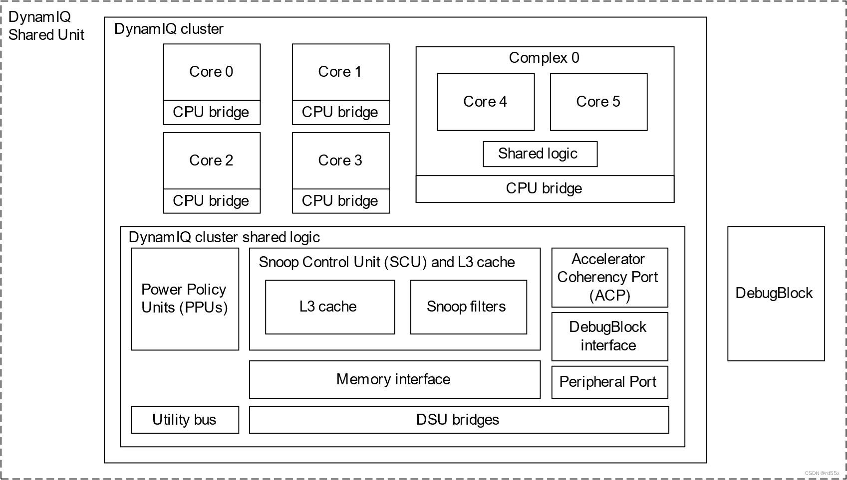
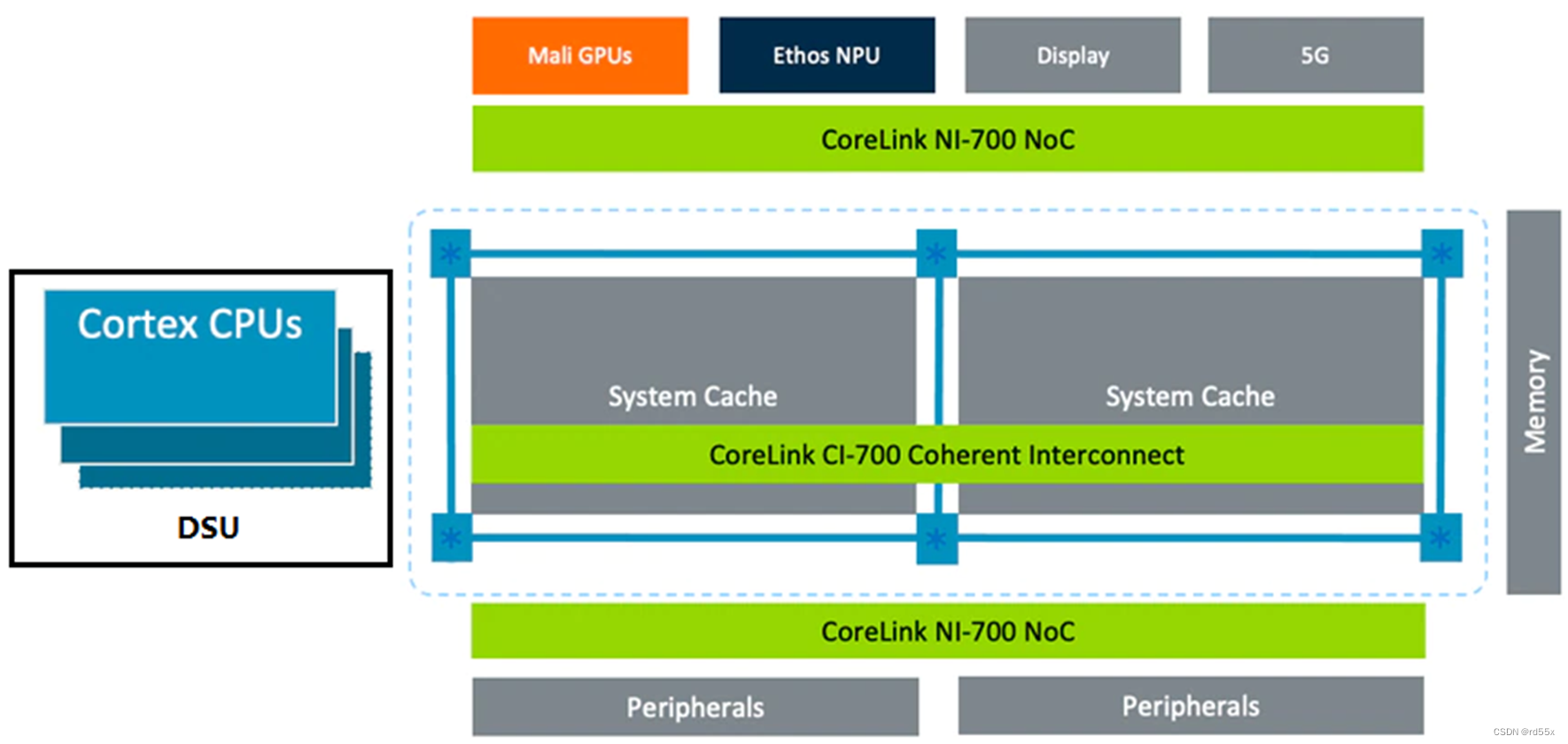
6. DynamIQ™ Shared Unit-110
所有 Armv9 Cortex CPU 都可以通过全新的 DynamIQ Shared Unit-110 (DSU-110) 在不同的 CPU 集群配置中绑定在一起。这种可配置集群方法的多功能性可满足从高端智能手机和笔记本电脑到 DTV 和可穿戴设备的各种市场需求。这构成了新的全面计算解决方案的支柱,该解决方案在多个消费设备市场和用例中提供不同级别的性能、效率和可扩展性的最新 Armv9 功能。
Arm DynamIQ Shared Unit-110 Technical Reference Manual r2p1
DSU-110 提供共享 L3 内存系统(shared L3 memory system)、探听控制和过滤(snoop control and filtering)以及其他控制逻辑,以支持 A 级架构内核集群,该集群称为 DSU-110 DynamIQ™ 集群。
DSU-110 DynamIQ™ 集群由 1 到 8 个内核组成,同一集群中最多可包含三种不同类型的内核。
DSU-110 DynamIQ™ Cluster Interfaces
DSU-110 管理片上系统 (SoC) 的所有外部接口,包括来自集群中 cores 和 complexes 的接口。
参考
- arm_cortex_x2_trm_101803_0200_06_en.pdf
- arm_cortex_a710_core_trm_101800_0201_07_en.pdf
- arm_cortex_a510_core_trm_101604_0003_16_en.pdf
- Arm_Cortex-X2_Core_Software_Optimization_Guide.pdf
- Arm_Cortex-A710_Core_Software_Optimization_Guide.pdf
- arm_cortex-a510_core_software_optimization_guide.pdf
- arm_dsu_110_trm_102639_0201_01_en.pdf
- First Armv9 Cortex CPUs for Consumer Compute - Architectures and Processors blog - Arm Community blogs - Arm Community


 1127
1127

 被折叠的 条评论
为什么被折叠?
被折叠的 条评论
为什么被折叠?
 到【灌水乐园】发言


