


FPGA 综合笔记
仿真时阻塞赋值和非阻塞赋值
Use of Non-Blocking Assignment in Testbench : Verilog
https://stackoverflow.com/questions/33536177/use-of-non-blocking-assignment-in-testbench-verilog
non-blocking assignment does not work as expected in Verilog
https://electronics.stackexchange.com/questions/84341/non-blocking-assignment-does-not-work-as-expected-in-verilog
This is actually quite similar to a question I answered previously, but I will try to build up a canonical answer for this somewhat common issue.
In a zero-delay simulation like this, the test flip-flop has a setup time and a hold time of zero:
```math
Tsetup=Thold=0
```
What this means is that the instant the sensitive clock edge occurs, the output is updated, regardless of what happened immediately before or after that instant. This is not like real hardware which would usually have a non-zero 𝑇𝑠𝑒𝑡𝑢𝑝 and 𝑇ℎ𝑜𝑙𝑑.
I ran your testbench, and the results are pretty clear. The valid signal changes at the same time the clock signal does. You have delayed them by precisely the same amount. So at the very edge when the clock is high, the valid signal has also changed:
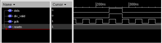
Both the input (div_valid), and the clock (gclk) go high at the same time: 220 ns. Therefore, the DFF latches this new data, and the output changes instantly since there is also 0 propagation delay. This simulation would look less confusing if we just chose a different delay value for the input to the design:
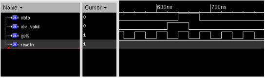
In this case, we update the input on the falling edge of the clock (620 ns). It is much more clear now that the next clock edge (640 ns) will be when the DFF updates its output.
Curious state transitions in state machine RTL simulation
https://electronics.stackexchange.com/questions/76647/curious-state-transitions-in-state-machine-rtl-simulation/76651#76651
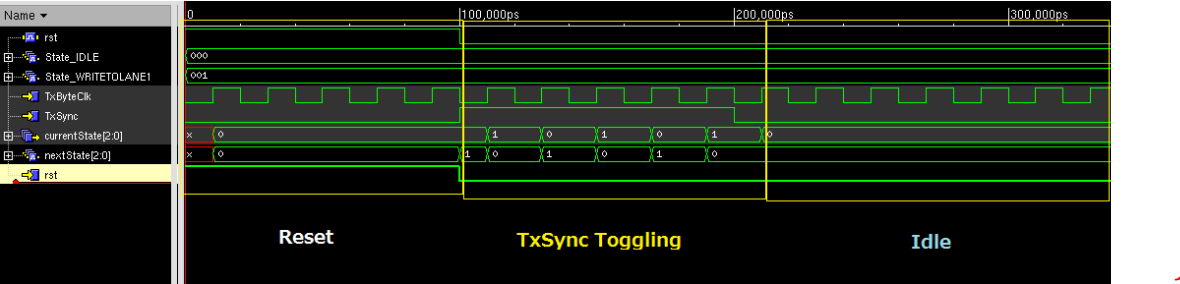
Pitfall: If your testbench updates the TxSync input exactly at the rising clock edge, You will just have a glitch in nextState. Your simulator may remove this glitch, making it look like nextState never entered State_WRITETOLANE1, when in fact it did, just for a very brief moment. This would make it look like currentState latched a value that nextState never had.
Remedy: Don’t update the inputs exactly at the rising clock edge. Add some small delay so that the simulation can be more clearly understood. In my case, I updated the input at the falling clock edge. But the update time is arbitrary if you are doing a 0 delay simulation.
陷阱:如果您的测试台在上升的时钟边缘精确更新了 TxSync 输入,那么 nextState 中将会出现一个毛刺。您的模拟器可能会消除这个毛刺,使其看起来 nextState 从未进入过 State_WRITETOLANE1 状态,但实际上它确实进入过,只是非常短暂。这会让它看起来 currentState 捕获了一个 nextState 从未拥有的值。
解决方法:不要在上升的时钟边缘精确更新输入。增加一些小延迟,以便模拟更清晰地理解。在我的情况下,我是在下降的时钟边缘更新输入的。但如果您正在进行零延迟模拟,更新时间是任意的。
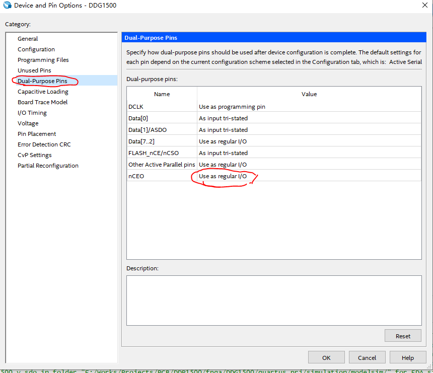
Quartus 编译错误
Can’t place multiple pins assigned to pin location
Error (176310): Can’t place multiple pins assigned to pin location Pin_101 (IOPAD_X34_Y18_N21)
Info (176311): Pin ch1_dac[3] is assigned to pin location Pin_101 (IOPAD_X34_Y18_N21)
Info (176311): Pin ALTERA_nCEO is assigned to pin location Pin_101 (IOPAD_X34_Y18_N21)
解决办法:
菜单->Assignments->Device->Device and Pin Options:
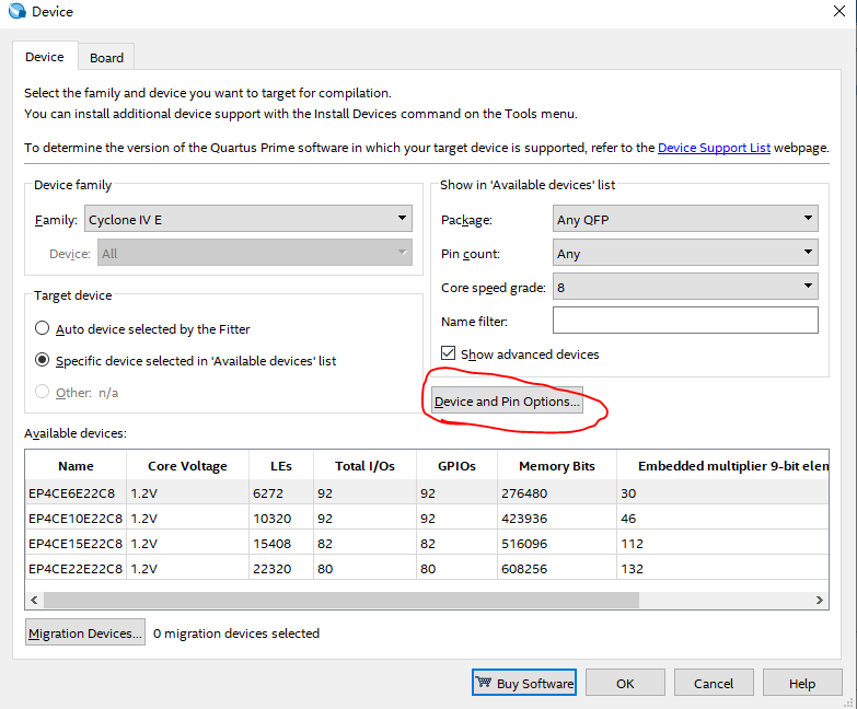
将相关引脚改为普通 IO:
仿真通过,上板验证失败
解决办法:板子断电,上电,再烧录
一个可能的原因:FPGA 器件支持除法吗?
固化程序启动失败
故障描述
EP4CE6E22C8 通过 jic 文件固化成功,但是启动失败,FPGA 的 CONF_DONE 引脚输出总是低。实际该引脚在配置期间为低,配置成功后为高。
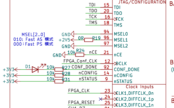
启动失败板子:带10k 上电阻,CONIFG_DONE 脚对地95M电阻,对VCC电阻:32k
启动 OK 的板子:CONFIG_DONE 脚对比:102M,, 对 VCC电阻:102M
故障原因
怀疑1:板子 FPGA 引脚有四根分线,怀疑是飞线过多,在操作时烧了板子。
怀疑2: CONF_DONE 引脚的 R27、D1 是手焊的,可能在焊接时烧了板子?
尝试
测量 FPGA 晶振频率: OK
尝试重新焊接 R19 ,失败
尝试更换 W25Q16: 失败
尝试重新编译: 失败
FPGA 坏了,只能更换FPGA
DDS
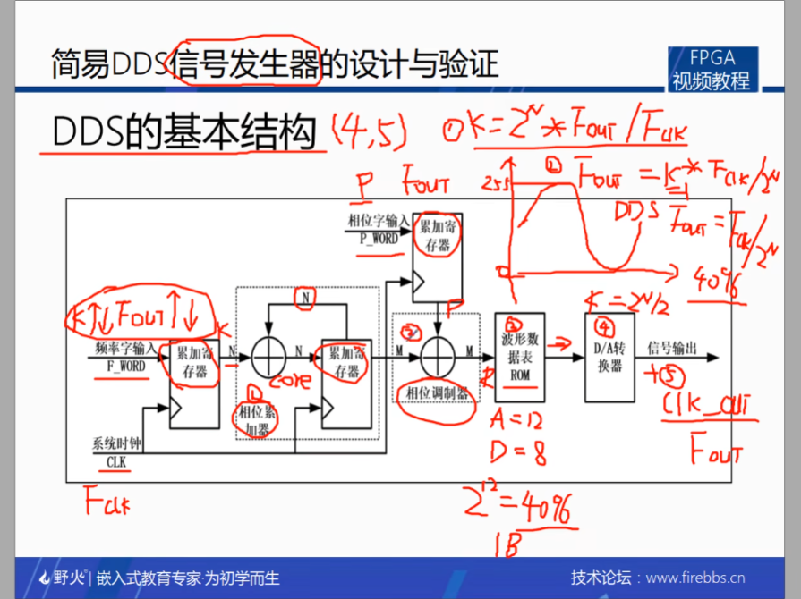
输出信号和频率字 K 的关系:
F
O
U
T
=
K
×
F
C
L
K
2
N
F_{OUT} = \frac{K \times F_{CLK}}{2^N}
FOUT=2NK×FCLK
其中:
K :频率字
N: K 的位宽
K 值越大,输出频率 FOUT 越大。
K 值越小,输出频率 FOUT 越小。
K 最小为1, 最大为:
2
N
2
\frac{2^N}{2}
22N
当 K 最小时,可以得到 DDS 的最小分辨率:
F
O
U
T
=
F
C
L
K
2
N
F_{OUT} = \frac{F_{CLK}}{2^N}
FOUT=2NFCLK
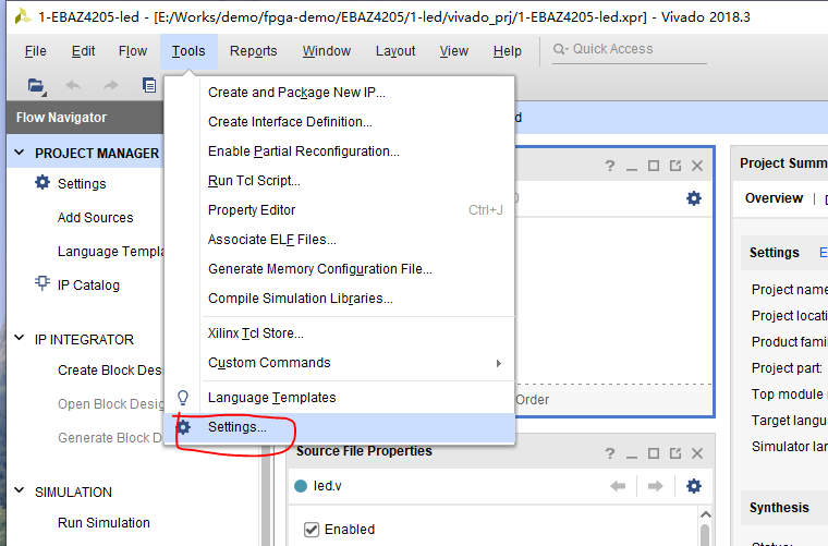
Vivado 中使用外部编辑器 Notepad++ 打开源文件
-
在 Vivado 的主界面中,点击左上角的 Tools 菜单。
-
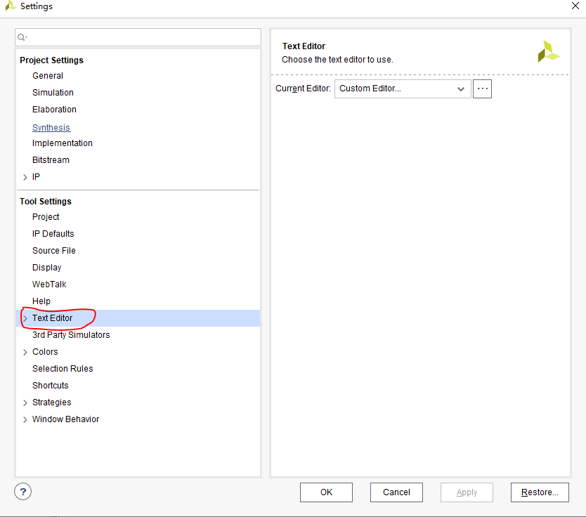
在 Vivado 的设置窗口中,寻找并点击 Text Editor 选项:
-
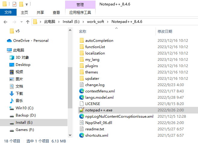
在继续之前,需要先找到 Notepad++ 的安装目录。可以通过文件资源管理器手动导航到 Notepad++ 的安装文件夹,或者通过右键点击 Notepad++ 的快捷方式选择“属性”来查看“起始位置”(这取决于你的操作系统和设置):
-
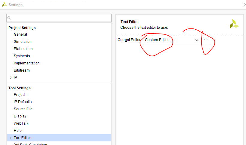
选择 Custom Editor ,点击 … 路径设置:
-
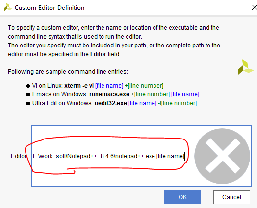
在指定的输入框中粘贴你刚才复制的 Notepad++ 安装路径,,你可能需要将正斜杠(/)改为反斜杠(\)在路径的末尾添加
notepad++.exe [file name](注意,[file name]是一个占位符,表示 Vivado 将通过命令行参数传递给 Notepad++ 的文件名):
+VX: jiyuyun18, 留言:FPGA, 加入 FPGA 技术交流群


 9173
9173

 被折叠的 条评论
为什么被折叠?
被折叠的 条评论
为什么被折叠?
 到【灌水乐园】发言


