


Please indicate the source: http://blog.csdn.net/gaoxiangnumber1
Welcome to my github: https://github.com/gaoxiangnumber1
5.1 PRINCIPLES OF I/O HARDWARE
5.1.1 I/O Devices
- I/O devices can be divided into two categories: block devices and character devices.
- A block device is one that stores information in fixed-size blocks, each one with its own address. Common block sizes range from 512 to 65536 bytes. All transfers are in units of one or more entire(consecutive) blocks. The essential property of a block device is that it is possible to read or write each block independently of all the other ones. Hard disks and USB sticks are block devices.
- A character device delivers or accepts a stream of characters without regard to any block structure. It isn’t addressable and doesn’t have any seek operation. Printers and network interfaces can be seen as character devices.
- However, some devices do not fit in this classification scheme. Clocks are neither block addressable nor do they generate or accept character streams. All they do is cause interrupts at well-defined intervals.
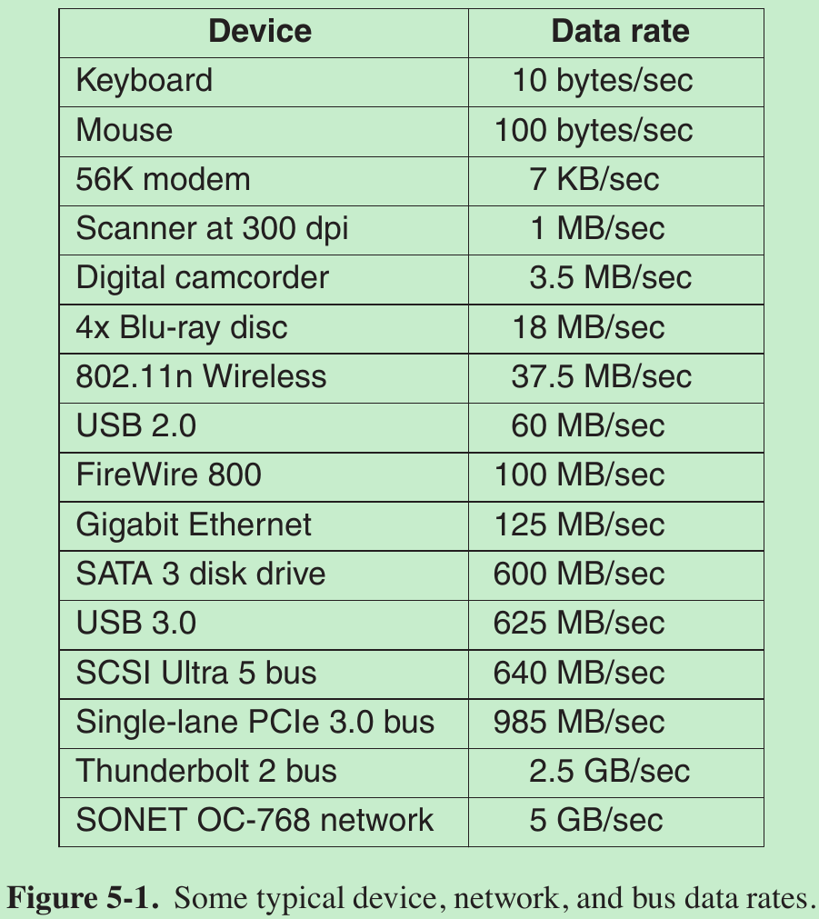
- I/O devices cover a huge range in speeds(Figure 5-1).
5.1.2 Device Controllers
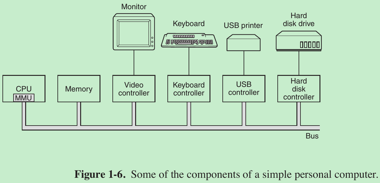
- I/O units often consist of a mechanical component(the device itself) and an electronic component(called the device controller or adapter). Fig. 1-6.
- The controller card usually has a connector on it, into which a cable leading to the device itself can be plugged. The interface between the controller and the device is often a low-level one.
- The controller’s job is to convert the serial bit stream into a block of bytes and perform any error correction necessary. The block of bytes is typically first assembled, bit by bit, in a buffer inside the controller. After its checksum has been verified and the block has been declared to be error free, it can then be copied to main memory.
5.1.3 Memory-Mapped I/O
- Each controller has a few registers that are used for communicating with the CPU.
- By writing into these registers, the OS can command the device to deliver data, accept data, switch itself on or off, or otherwise perform some action.
- By reading from these registers, the OS can learn what the device’s state is, whether it is prepared to accept a new command, and so on.
- In addition to the control registers, many devices have a data buffer that the OS can read and write. E.g., a common way for computers to display pixels on the screen is to have a video RAM, which is a data buffer, available for programs or the OS to write into.

- Two alternatives for CPU to communicates with the control registers and the device data buffers.
- Each control register is assigned an I/O port number, an 8- or 16-bit integer. The set of all the I/O ports form the I/O port space which is protected so that only OS can access it. The address spaces for memory and I/O are different(Fig. 5-2(a)).
E.g., usingIN REG, PORT, the CPU can read in control register PORT and store the result in CPU register REG. - Map all the control registers into the memory space(Fig. 5-2(b)). Each control register is assigned a unique memory address to which no memory is assigned. This system is called memory-mapped I/O.
- Each control register is assigned an I/O port number, an 8- or 16-bit integer. The set of all the I/O ports form the I/O port space which is protected so that only OS can access it. The address spaces for memory and I/O are different(Fig. 5-2(a)).
- The x86 uses a hybrid scheme, with memory-mapped I/O data buffers and separate I/O ports for the control registers(Fig. 5-2(c)).
- How do these schemes work in practice?
- When the CPU wants to read a word, either from memory or from an I/O port, it puts the address it needs on the bus’ address lines and then asserts a READ signal on a bus’ control line.
- A second signal line is used to tell whether I/O space or memory space is needed.
-1- If it is memory space, the memory responds to the request.
-2- If it is I/O space, the I/O device responds to the request.
-3- If there is only memory space, every memory module and every I/O device compares the address lines to the range of addresses that it services. If the address falls in its range, it responds to the request. Since no address is assigned to both memory and an I/O device, there is no conflict.
Advantages of memory-mapped I/O.
- If special I/O instructions are needed to read and write the device control registers, access to them requires the use of assembly code since there is no way to execute an IN or OUT instruction in C. Calling such a procedure adds overhead to controlling I/O. With memory-mapped I/O, device control registers are just variables in memory and can be addressed in C the same way as any other variables.
Summary: An I/O device driver can be written entirely in C with memory-mapped I/O, otherwise assembly code is needed. - No special protection mechanism is needed to keep user processes from performing I/O. All the OS has to do is refrain from putting that portion of the address space containing the control registers in any user’s virtual address space.
- Every instruction that can reference memory can also reference control registers. E.g., The instruction
TESTthat tests a memory word for 0 can also be used to test a control register for 0. Without memory-mapped I/O, the control register must first be read into the CPU, then tested, requiring two instructions instead of one, thus slowing down the responsiveness of detecting an device.
LOOP:   TEST PORT 4     // check if port 4 is 0
        BEQ READY       // if it is 0, go to ready
        BRANCH LOOP // otherwise, continue testing
READY:
Disadvantages of memory-mapped I/O.
- Since most computers cache memory words, caching a device control register would be disastrous. For the above codes: The first reference to PORT 4 would cause it to be cached. Subsequent references would take the value from the cache and not ask the device. When the device became ready, the software would have no way of finding out. So, the loop would go on forever.
Solution: the hardware has to be able to selectively disable caching on a per-page basis. This feature adds extra complexity to both the hardware and the OS.
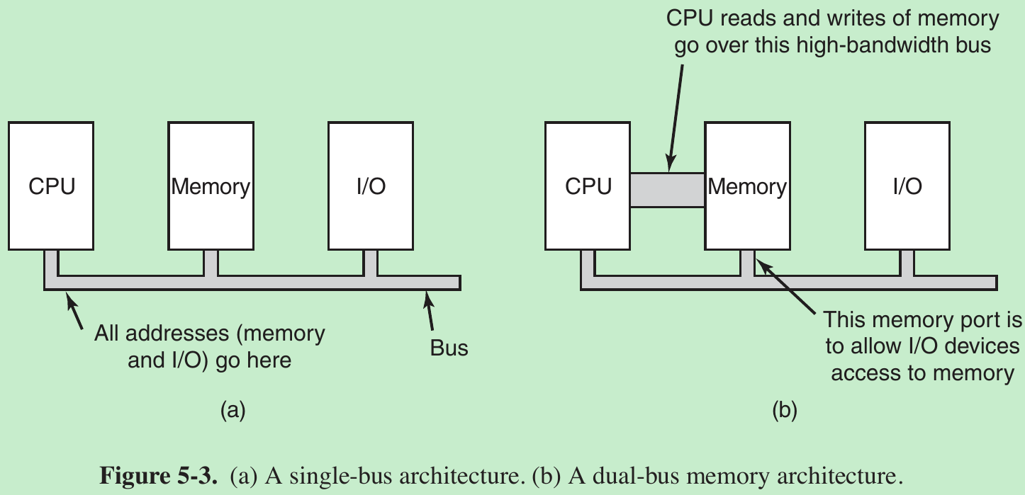
- If there is only one address space, then all memory modules and all I/O devices must examine all memory references to see which ones to respond to.
-1- If the computer has a single bus(Fig. 5-3(a)), having everyone look at every address is straightforward.
-2- But modern computers have a dedicated high-speed memory bus(Fig. 5-3(b)). The trouble is that the I/O devices have no way of seeing memory addresses as they go by on the memory bus, so they can’t respond to them.
Solution: First send all memory references to the memory, if the memory fails to respond, then the CPU tries the other buses. This design requires additional hardware complexity.
5.1.4 Direct Memory Access
- A DMA controller has access to the system bus independent of the CPU. It contains several registers that can be written and read by the CPU. These include a memory address register, a byte count register, and one or more control registers that specify the I/O port to use, the direction of the transfer(reading from or writing to the I/O device), the transfer unit(byte at a time or word at a time), and the number of bytes to transfer in one burst.
- How disk reads occur when DMA isn’t used.
- The disk controller reads the block from the drive serially, bit by bit, until the entire block is in the controller’s internal buffer.
- It computes the checksum to verify that no read errors have occurred.
- The controller causes an interrupt.
- The OS starts running, it can read the disk block from the controller’s buffer a byte or a word at a time by executing a loop, with each iteration reading one byte or word from a controller device register and storing it in main memory.
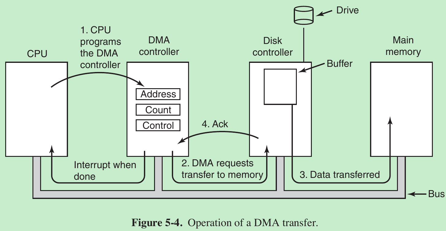
- When DMA is used:
- The CPU programs the DMA controller by setting its registers so it knows what to transfer where(step 1). It also issues a command to the disk controller telling it to read data from the disk into its internal buffer and verify the checksum. When valid data are in the disk controller’s buffer, DMA can begin.
- The DMA controller initiates the transfer by issuing a read request over the bus to the disk controller(step 2). The memory address to write to is on the bus’ address lines, so when the disk controller fetches the next word from its internal buffer, it knows where to write it.
- The write to memory is another standard bus cycle(step 3).
- When the write is complete, the disk controller sends an acknowledgement signal to the DMA controller over the bus(step 4). The DMA controller then increments the memory address to use and decrements the byte count.
- If the byte count is still greater than 0, steps 2 through 4 are repeated until the count reaches 0. At that time, the DMA controller interrupts the CPU to let it know that the transfer is now complete. When the OS starts up, it doesn’t have to copy the disk block to memory; it is already there.
- Many buses can operate in two modes: word-at-a-time mode and block mode. Some DMA controllers can operate in either mode.
- In word-at-a-time mode, the operation is as described above: the DMA controller requests the transfer of one word and gets it. If the CPU also wants the bus, it has to wait. The mechanism is called cycle stealing because the device controller steals an occasional bus cycle from the CPU once in a while, delaying it slightly.
- In block mode, the DMA controller tells the device to acquire the bus, issue a series of transfers, then release the bus. This is called burst mode. It is more efficient than cycle stealing because acquiring the bus takes time and multiple words can be transferred for the price of one bus acquisition. The down side to burst mode is that it can block the CPU and other devices for a substantial period if a long burst is being transferred.
-
- Most DMA controllers use physical memory addresses for their transfers. Using physical addresses requires the OS to convert the virtual address of the intended memory buffer into a physical address and write this physical address into the DMA controller’s address register.
- The other scheme is to write virtual addresses into the DMA controller. Then the DMA controller must use the MMU to have the virtual-to-physical translation done. Only if the MMU is part of the memory rather than part of the CPU, can virtual addresses be put on the bus.
- Recall that the disk first reads data into its internal buffer before DMA can start. Why does it need an internal buffer?
- By doing internal buffering, the disk controller can verify the checksum before starting a transfer. If the checksum is incorrect, an error is signaled and no transfer is done.
- Once a disk transfer has started, the bits keep ar
 最低0.47元/天 解锁文章


 1888
1888


 被折叠的 条评论
为什么被折叠?
被折叠的 条评论
为什么被折叠?
 到【灌水乐园】发言


