


以前一直使用别人成功的FMD,早几天对一些细节以及编程方法一无所知,同时也有很多人问我flash相关问题,我好想在论坛指点江山,给养技术,可是感觉有些东西确实需要补补,今天就看个明白吧。
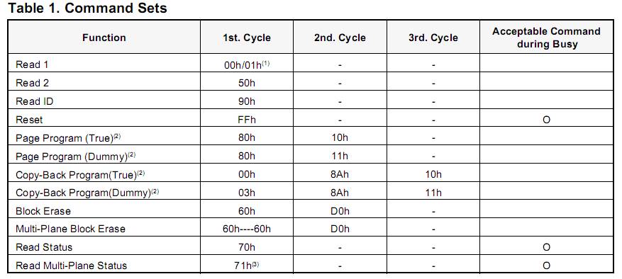
NAND Flash Technical Notes
Invalid Block(s)
Invalid blocks are defined as blocks that contain one or more invalid bits whose reliability is not guaranteed by Samsung. The infor-
mation regarding the invalid block(s) is so called as the invalid block information. Devices with invalid block(s) have the same quality
level or as devices with all valid blocks and have the same AC and DC characteristics. An invalid block(s) does not affect the perfor-
mance of valid block(s) because it is isolated from the bit line and the common source line by a select transistor. The system design
must be able to mask out the invalid block(s) via address mapping.(系统必须标记坏块) The 1st block, which is placed on 00h block address, is fully guaranteed to be a valid block, does not require Error Correction.(第一个block也就是00h block地址,厂家会保证绝对是好的,不用检查标记)
Identifying Invalid Block(s) 标记坏块
All device locations are erased(FFh) except locations where the invalid block(s) information is written prior to shipping. The invalid block(s) status is defined by the 6th byte in the spare area. Samsung makes sure that either the 1st or 2nd page of every invalid
block has non-FFh data at the column address of 517.(这是生产过程中产生的坏块,一般芯片原厂都会在出厂时都会将坏块第一个page的spare area的第6个byte标记为不等于0xff的值。) Since the invalid block information is also erasable in most cases, it is impos-
sible to recover the information once it has been erased. Therefore, the system must be able to recognize the invalid block(s) based
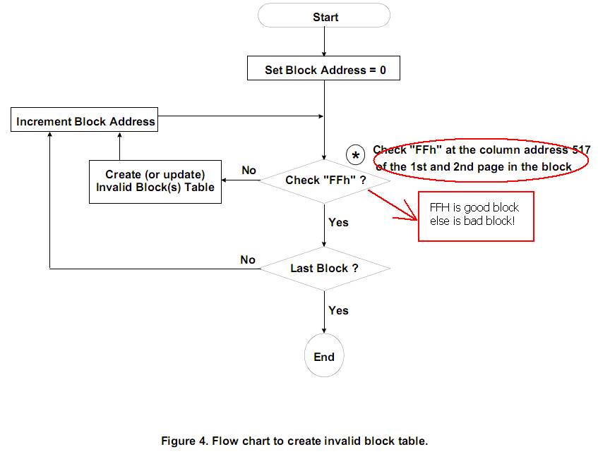
on the original invalid block information and create the invalid block table via the following suggested flow chart(Figure 4). Any inten-
tional erasure of the original invalid block information is prohibited.
怎么写程序识别坏块呢?请看下图。
现在来看看FMD驱动中的flash检测坏块函数
- /*************************************************************************************************
- The way the Read1 and Read2 commands work is like a pointer set to either the main area or the spare area. The spare area of bytes 512 to 527 may be selectively accessed by writing the Read2 command. Addresses A0 to A3 set the starting address of the spare area while addresses A4 to A7 are ignored. Unless the operation is aborted, the page address is automatically incremented for sequential row read as in Read1 operation and spare sixteen bytes of each page may be sequentially read. The Read1 com-mand(00h/01h) is needed to move the pointer back to the main area.
- Nand Flash的寻址
- Nand Flash的地址寄存器把一个完整的Nand Flash地址分解成Column Address与Page Address.进行寻址。
- Column Address: 列地址。Column Address其实就是指定Page上的某个Byte,指定这个Byte其实也就是指定此页的读写起始地址。
- Paage Address:页地址。由于页地址总是以512Bytes对齐的,所以它的低9位总是0。确定读写操作是在Flash上的哪个页进行的。
- 检测坏块:带外数据的第六位是否是0xff,是是好的block ,否是是坏的。
- ******************************************************************************/
- static BOOL IsBlockBad(BLOCK_ID blockID)
- {
- DWORD dwPageID = (blockID+START_BLOCK) << 5;
- BOOL bRet = FALSE;
- BYTE wFlag;
- BOOL bLastMode = SetKMode(TRUE);
- NF_nFCE_L(); // Select the flash chip.
- NF_CLEAR_RB();
- NF_CMD(CMD_RESET); // Send reset command.
- NF_WAITRB(); // Wait for flash to complete command.
- // Issue the command
- NF_CMD(CMD_READ2);//0x50 read Spare Field
- // Set up address
- //#define VALIDADDR 0x05 // S3C2440aNAND
- NF_ADDR(VALIDADDR);// why?// Column = 5 代表列地址是5
- NF_ADDR((dwPageID) & 0xff);//
- NF_ADDR((dwPageID >> 8) & 0xff);
- if (NEED_EXT_ADDR)
- NF_ADDR((dwPageID >> 16) & 0xff);
- NF_WAITRB(); // Wait for flash to complete command.
- // Now get the byte we want
- wFlag = (BYTE) NF_RDDATA();
- // good block=0xff bad block!=0xff
- if(wFlag != 0xff) {
- bRet = TRUE;
- }
- // Disable the chip
- NF_nFCE_H();
- SetKMode (bLastMode);
- return bRet;
- }
其实还有一个标记坏块函数,这个函数就是在检测坏块的位置标记为非0xff即可,一般是0x00在这里不再赘述。
这几检测坏块函数是被另外一个直接和FAL联系的坏块调用的,那个函数太牛B,所以也要贴出来。
读MBR等都是在这里实现的,这个函数相当关键,盘符能否出现,以及是否检测过度都要看这个函数
- /*
- @func DWORD | FMD_GetBlockStatus | Returns the status of the specified block.
- @rdesc Block status (see fmd.h).
- @comm
- @xref
- */
- DWORD FMD_GetBlockStatus(BLOCK_ID blockID)
- {
- SECTOR_ADDR Sector = (blockID * NAND_PAGE_CNT);
- SectorInfo SI;
- DWORD dwResult = 0;
- if (IsBlockBad(blockID))// if It is true ,The block is bad
- return BLOCK_STATUS_BAD;
- if (!FMD_ReadSector(Sector, NULL, &SI, 1)) // read MBR !!! why I didn't know that?
- return BLOCK_STATUS_UNKNOWN;
- if (!(SI.bOEMReserved & OEM_BLOCK_READONLY))
- dwResult |= BLOCK_STATUS_READONLY;
- if (!(SI.bOEMReserved & OEM_BLOCK_RESERVED))
- dwResult |= BLOCK_STATUS_RESERVED;
- return(dwResult);
- }
对了,flash是如何擦除的呢?这个是以block为单位的。下面来看看
- /* 这么清楚,相比也不用注释了,这里和前面的不同前面是页地址,这里是块地址
- @func BOOL | FMD_EraseBlock | Erases the specified flash block.
- @rdesc TRUE = Success, FALSE = Failure.
- @comm
- @xref
- */
- BOOL FMD_EraseBlock(BLOCK_ID blockID)
- {
- BYTE Status;
- ULONG blockPage = ((blockID+START_BLOCK) * NAND_PAGE_CNT); // Convert block address to page address.
- BOOL bLastMode = SetKMode(TRUE);
- NF_nFCE_L(); // Select the flash chip.
- NF_WAITRB(); // Wait for flash to complete command.
- NF_CMD(CMD_RESET); // Send reset command.
- NF_WAITRB(); // Wait for flash to complete command.
- NF_CMD(CMD_ERASE); // Send block erase command.
- NF_ADDR(blockPage & 0xff); /* The mark of bad block is in 0 page */
- NF_ADDR((blockPage >> 8) & 0xff); /* For block number A[24:17] */
- if (NEED_EXT_ADDR)
- NF_ADDR((blockPage >> 16) & 0xff); /* For block number A[25] */
- NF_WAITRB(); // Wait for flash to complete command.
- NF_CMD(CMD_ERASE2); // Send block erase confirm command.
- NF_WAITRB(); // Wait for flash to complete command.
- do
- {
- NF_CMD(CMD_STATUS);
- Status = NF_RDDATA(); // Read command status.
- }while(!(Status & STATUS_READY));
- NF_nFCE_H(); // Deselect the flash chip.
- SetKMode (bLastMode);
- return((Status & STATUS_ERROR) ? FALSE : TRUE);
- }
对于这个命令发送原理,请看下图

这个就是针对页的时候,为什么先发列地址一次,然后发三次Row Address(page Address)了
现在真要仔细品味flash的原理了。
其实flash的难点在于ECC,明天再看FMD_WriteSector和FMD_ReadSector两个函数了。不过在下班之前
我要提示一下,这个优龙的bootloader flash的写法貌似有很大不同。到时候再来个比较吧。
————————————————————————————————————————
关于flash结构与编程的文档我已经上传到 CSDNhttp://download.csdn.net/source/895242
建议大家下来看看。
——FMD_WriteSector和FMD_ReadSector两个函数涉及的东西较多,我下篇文档会独立分析。
转载请标明:作者wogoyixikexie@gliet.桂林电子科技大学一系科协。如有错误,希望能够留言指出;如果你有更加好的方法,也请在博客后面留言,我会感激你的批评和分享。


 418
418

 被折叠的 条评论
为什么被折叠?
被折叠的 条评论
为什么被折叠?
 到【灌水乐园】发言


