


目录
3.1.5 DFF with asynchronous reset
3.1.14 Create circuit from truth table
3.1.18 Dual-edge triggered flip-flop
3.3.3 Left/right arithmetic shift by 1 or 8
3.4.3 Conway's Game of Life 16x16
3.5.1 Simple FSM 1 (asynchronous reset)
3.5.2 Simple FSM 1 (synchronous reset)
3.5.3 Simple FSM 2 (asynchronous reset)
3.5.4 Simple FSM 2 (synchronous reset)
3.5.5 Simple state transitions 3
Circuit
3 Sequential Logic
3.1 Latches and Flip-Flops
3.1.1 D Flip-Flop
A D flip-flop is a circuit that stores a bit and is updated periodically, at the (usually) positive edge of a clock signal.
D flip-flops are created by the logic synthesizer when a clocked always block is used (See alwaysblock2). A D flip-flop is the simplest form of "blob of combinational logic followed by a flip-flop" where the combinational logic portion is just a wire.
Create a single D flip-flop.
module top_module (
    input clk,    // Clocks are used in sequential circuits
    input d,
    output reg q );//
    always @(posedge clk)
        begin
           q <= d;
        end
    // Use a clocked always block
    // copy d to q at every positive edge of clk
    // Clocked always blocks should use non-blocking assignments
endmodule
3.1.2 D Flip-Flops
Create 8 D flip-flops. All DFFs should be triggered by the positive edge of clk.
module top_module (
    input clk,
    input [7:0] d,
    output [7:0] q
);
    always @(posedge clk)
        begin
           q <= d;
        end
endmodule
3.1.3 DFF with reset
Create 8 D flip-flops with active high synchronous reset. All DFFs should be triggered by the positive edge of clk.
module top_module (
    input clk,
    input reset,            // Synchronous reset
    input [7:0] d,
    output [7:0] q
);
    always @(posedge clk)
        begin
            if (reset)
                q <= 8'b00000000;
            else
                q <= d;
        end
endmodule
3.1.4 DFF with reset value
Create 8 D flip-flops with active high synchronous reset. The flip-flops must be reset to 0x34 rather than zero. All DFFs should be triggered by the negative edge of clk.
module top_module (
    input clk,
    input reset,
    input [7:0] d,
    output [7:0] q
);
    always @(negedge clk)
        begin
            if (reset)
                q <= 8'b00110100;
            else
                q <= d;
        end
endmodule
module top_module (
input clk,
input reset,
input [7:0] d,
output [7:0] q
);
always @(negedge clk)
begin
if (!reset)
q <= d;
else
q <= 8'b00110100;
end
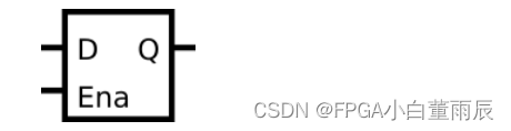
endmodule3.1.5 DFF with asynchronous reset
Create 8 D flip-flops with active high asynchronous reset. All DFFs should be triggered by the positive edge of clk.
module top_module (
    input clk,
    input areset,   // active high asynchronous reset
    input [7:0] d,
    output [7:0] q
);
    always @(posedge clk or posedge areset)
        begin
            if (areset)
                q <= 8'b00000000;
            else
                q <= d;
        end
endmodule
3.1.6 DFF with byte enable
Create 16 D flip-flops. It's sometimes useful to only modify parts of a group of flip-flops. The byte-enable inputs control whether each byte of the 16 registers should be written to on that cycle. byteena[1] controls the upper byte d[15:8], while byteena[0] controls the lower byte d[7:0].
resetn is a synchronous, active-low reset.
All DFFs should be triggered by the positive edge of clk.
module top_module (
    input clk,
    input resetn,
    input [1:0] byteena,
    input [15:0] d,
    output [15:0] q
);
    always @(posedge clk)
        begin
            if (!resetn)
                q <= 16'b0;
            else
                begin
                    q[7:0] <= byteena[0] ? d[7:0] : q[7:0];
                    q[15:8] <= byteena[1] ? d[15:8] : q[15:8];
                end
        end
endmodule
3.1.7 D Latch
Implement the following circuit:
Note that this is a latch, so a Quartus warning about having inferred a latch is expected.
module top_module (
    input d,
    input ena,
    output q);
    always @(*)
        begin
            if(ena)
                q <= d;
            else
                q <= q;
        end
endmodule
3.1.8 DFF
Implement the following circuit:
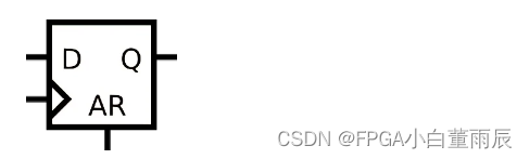
module top_module (
    input clk,
    input d,
    input ar,   // asynchronous reset
    output q);
    always @(posedge clk or posedge ar)
        begin
            if(ar)
                q <= 1'b0;
            else
                q <= d;
        end
endmodule
3.1.9 DFF
Implement the following circuit:
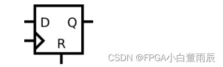
module top_module (
    input clk,
    input d,
    input r,   // synchronous reset
    output q);
    always @(posedge clk)
        begin
            if(r)
                q <= 1'b0;
            else
                q <= d;
        end
endmodule
3.1.10 DFF+gate
Implement the following circuit:
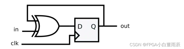
module top_module (
    input clk,
    input in,
    output out);
    always @(posedge clk)
        begin
            out <= in ^ out ;
        end
endmodule
3.1.11 Mux and DFF
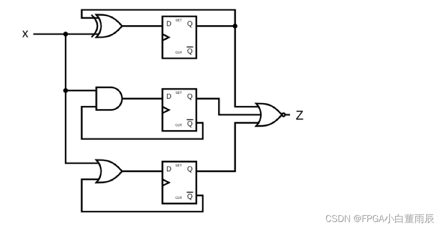
Taken from ECE253 2015 midterm question 5
Consider the sequential circuit below:
Assume that you want to implement hierarchical Verilog code for this circuit, using three instantiations of a submodule that has a flip-flop and multiplexer in it. Write a Verilog module (containing one flip-flop and multiplexer) named top_module for this submodule.
实现一个带触发器的多路选择器
module top_module (
	input clk,
	input L,
	input r_in,
	input q_in,
	output reg Q);
    always @(posedge clk)
        begin
            Q <= (L) ? r_in : q_in;
        end
endmodule
3.1.12 Mux and DFF
Consider the n-bit shift register circuit shown below:
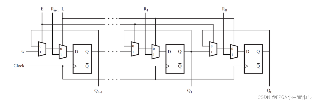
Write a Verilog module named top_module for one stage of this circuit, including both the flip-flop and multiplexers.
module top_module (
    input clk,
    input w, R, E, L,
    output Q
);
    always @(posedge clk)
        begin
            Q <= (L) ? R : ((E) ? w : Q);
        end
endmodule
3.1.13 DFFs and gates
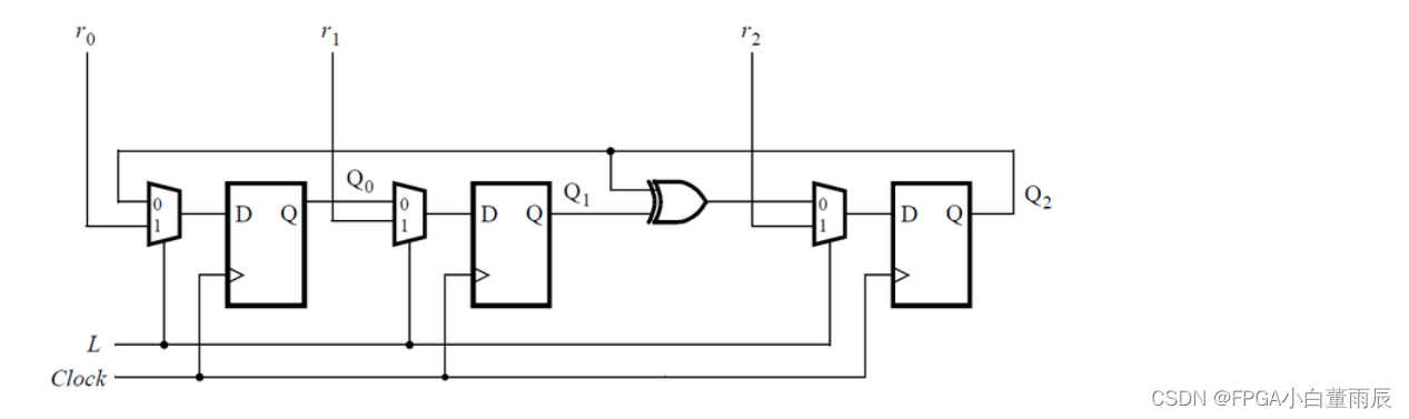
Given the finite state machine circuit as shown, assume that the D flip-flops are initially reset to zero before the machine begins.
Build this circuit.
module top_module (
    input clk,
    input x,
    output z
);
    wire Q1,Q2,Q3;
    always @(posedge clk)
        begin
            Q1 <= x ^ Q1;
            Q2 <= x & ~Q2;
            Q3 <= x | ~Q3;
        end
    assign z = ~(Q1 | Q2 | Q3);
endmodule
3.1.14 Create circuit from truth table
A JK flip-flop has the below truth table. Implement a JK flip-flop with only a D-type flip-flop and gates. Note: Qold is the output of the D flip-flop before the positive clock edge.
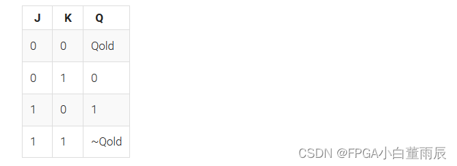
module top_module (
    input clk,
    input j,
    input k,
    output Q);
    always @(posedge clk)
        begin
            case({j,k})
                2'b00 : Q <= Q;
            	2'b01 : Q <= 1'b0;
            	2'b10 : Q <= 1'b1;
                2'b11 : Q <= ~Q;
            endcase
        end
endmodule
3.1.15 Detect an edge
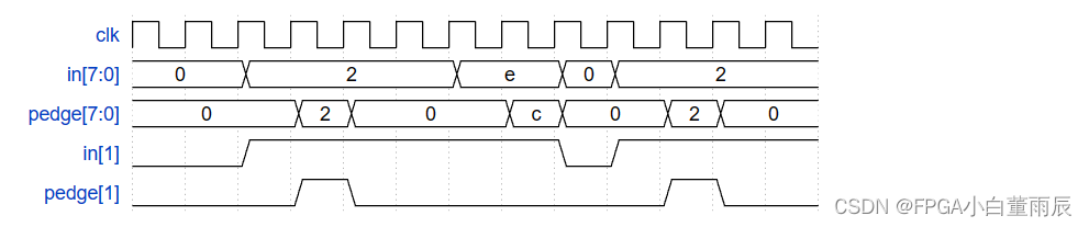
For each bit in an 8-bit vector, detect when the input signal changes from 0 in one clock cycle to 1 the next (similar to positive edge detection). The output bit should be set the cycle after a 0 to 1 transition occurs.
Here are some examples. For clarity, in[1] and pedge[1] are shown separately.
检测上升沿,并在下一个时钟周期输出1
module top_module (
    input clk,
    input [7:0] in,
    output [7:0] pedge
);
    reg [7:0] temp_in;
    always @(posedge clk)
        begin
            temp_in <= in;
            pedge <= ~temp_in & in;//左向量取反与右向量相与,可实现上升沿检测,并滞后一拍输出
        end
endmodule 最低0.47元/天 解锁文章


 1万+
1万+


 被折叠的 条评论
为什么被折叠?
被折叠的 条评论
为什么被折叠?
 到【灌水乐园】发言


