


目录
5. DFF with asynchronous reset
14. Create circuit from truth table
18. Dual-edge triggered flip-flop
3.2 Sequential Logic
3.2.1 Latches and Flip-Flops
1. D flip-flop
A D flip-flop is a circuit that stores a bit and is updated periodically, at the (usually) positive edge of a clock signal.

D flip-flops are created by the logic synthesizer when a clocked always block is used (See alwaysblock2). A D flip-flop is the simplest form of "blob of combinational logic followed by a flip-flop" where the combinational logic portion is just a wire.
module top_module (
    input clk,    // Clocks are used in sequential circuits
    input d,
    output reg q );//

    // Use a clocked always block
    //   copy d to q at every positive edge of clk
    //   Clocked always blocks should use non-blocking assignments

    always @(posedge clk)begin
       q<=d;
    end
endmodule
2. D flip-flops
Create 8 D flip-flops. All DFFs should be triggered by the positive edge of clk.
module top_module (
    input clk,
    input [7:0] d,
    output [7:0] q
);
    always @(posedge clk)begin
        q<=d;

    end

endmodule
3. DFF with reset
Create 8 D flip-flops with active high synchronous reset. All DFFs should be triggered by the positive edge of clk.
module top_module (
    input clk,
    input reset,            // Synchronous reset
    input [7:0] d,
    output [7:0] q
);

    always @(posedge clk)begin
        if (reset)begin
            q<=8'd0;
        end
        else begin
            q<=d;
        end
    end
endmodule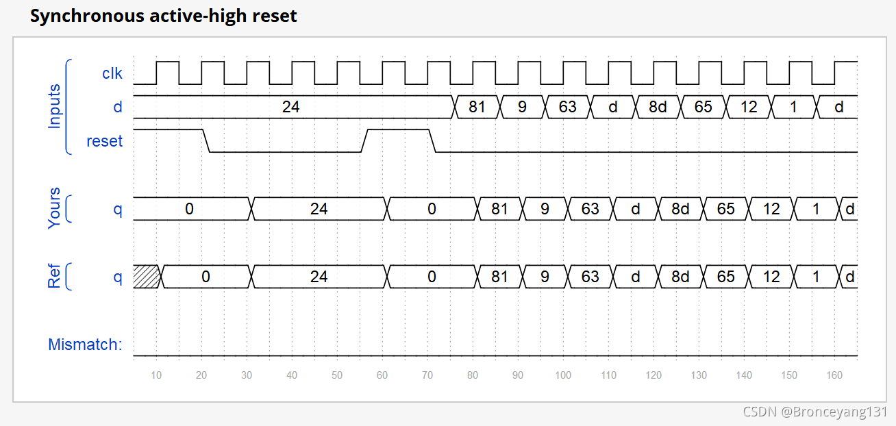
4. DFF with reset value
Create 8 D flip-flops with active high synchronous reset. The flip-flops must be reset to 0x34 rather than zero. All DFFs should be triggered by the negativeedge of clk.
module top_module (
    input clk,
    input reset,
    input [7:0] d,
    output [7:0] q
);
    always @(negedge clk)begin
        if (reset)begin
            q<=8'h34;
        end
        else begin
            q<=d;
        end
    end

endmodule
5. DFF with asynchronous reset
Create 8 D flip-flops with active high asynchronous reset. All DFFs should be triggered by the positive edge of clk.
module top_module (
    input clk,
    input areset,   // active high asynchronous reset
    input [7:0] d,
    output [7:0] q
);
    always @(posedge clk ,posedge areset)begin
        if (areset)begin
            q<=8'd0;
        end
        else begin
            q<=d;
        end
    end

endmodule
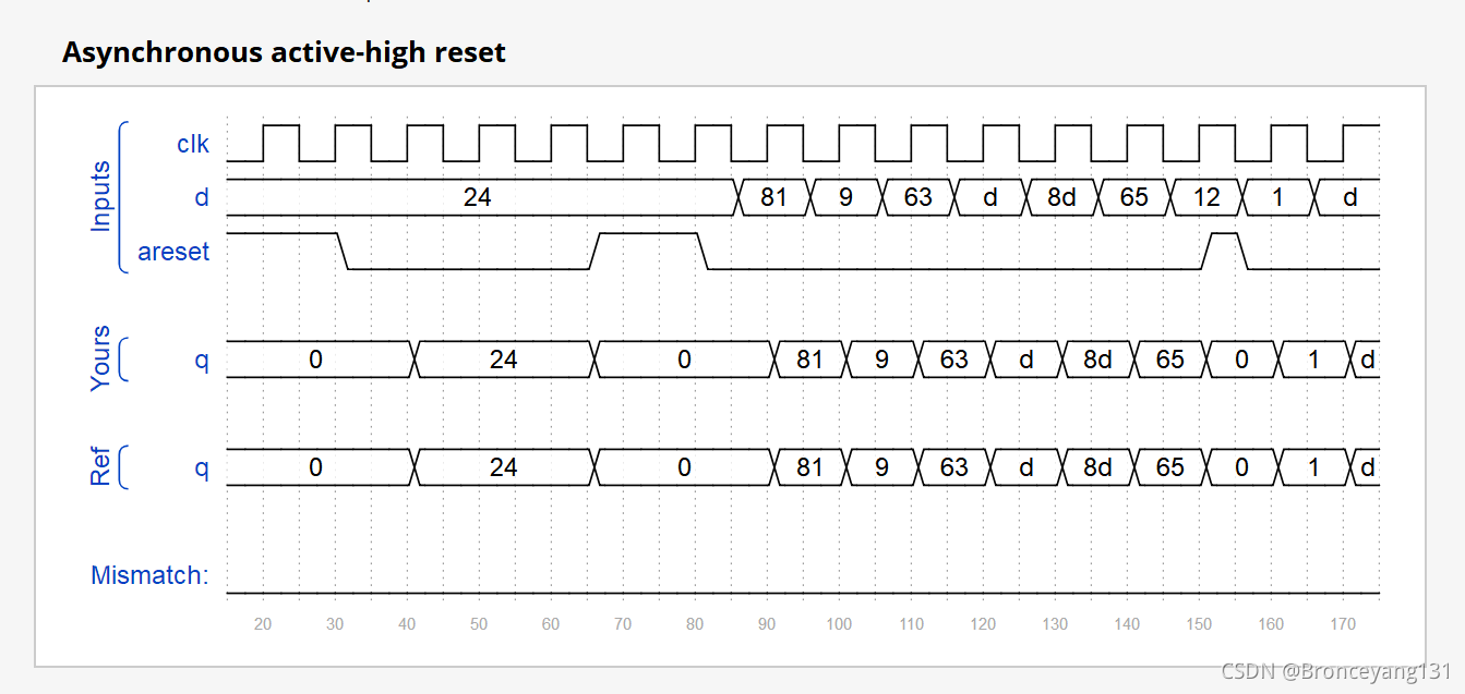
与同步复位相比,异步复位信号一来,输出信号立马变化。
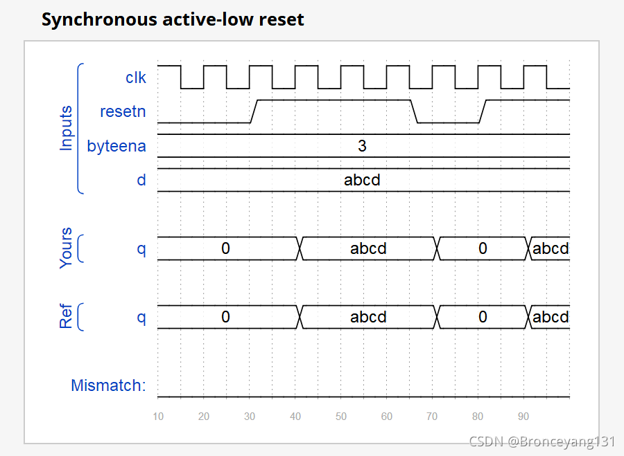
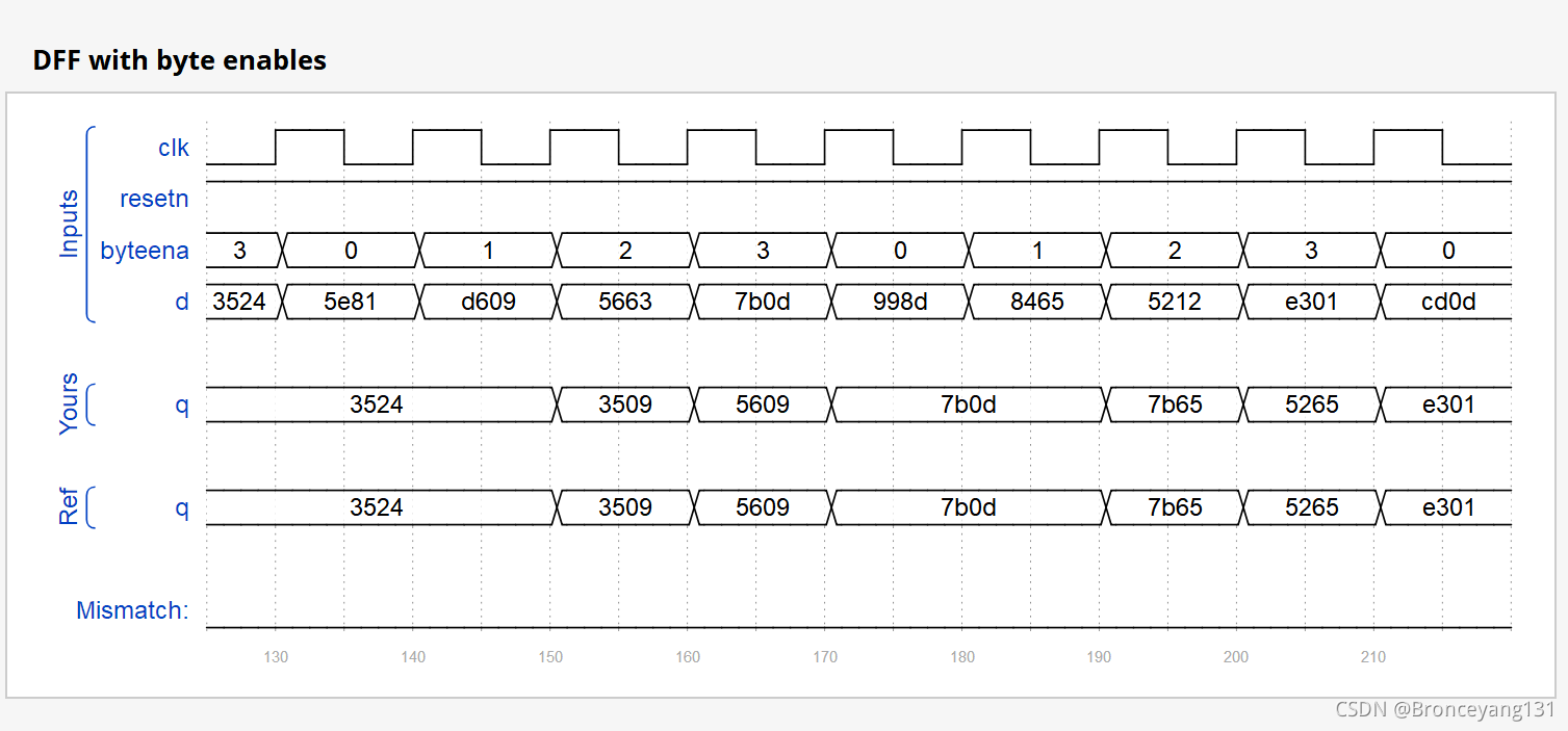
6. DFF with byte enable
Create 16 D flip-flops. It's sometimes useful to only modify parts of a group of flip-flops. The byte-enable inputs control whether each byte of the 16 registers should be written to on that cycle. byteena[1] controls the upper byte d[15:8], while byteena[0] controls the lower byte d[7:0].
resetn is a synchronous, active-low reset.
All DFFs should be triggered by the positive edge of clk.
module top_module (
    input clk,
    input resetn,
    input [1:0] byteena,
    input [15:0] d,
    output [15:0] q
);
    always @(posedge clk)begin
        if(!resetn)begin
           q<=16'd0;
        end
        else begin
            if(byteena[1]&&byteena[0])begin
                q<=d;
            end
            else if (byteena[1] && ~byteena[0])begin
                q[15:8]<=d[15:8];
            end
            else if (~byteena[1] && byteena[0])begin
                q[7:0]<=d[7:0];
            end
            else begin
                q<=q;
            end
    end
    end
endmodule
仿真结果:
7. D Latch
Implement the following circuit:

Note that this is a latch, so a Quartus warning about having inferred a latch is expected.
module top_module (
    input d,
    input ena,
    output q);
assign q=ena?d:q;

endmodule
8. DFF
Implement the following circuit,异步复位。

module top_module (
    input clk,
    input d,
    input ar,   // asynchronous reset
    output reg q);


    always @(posedge clk or posedge  ar)begin
        if(ar) begin
            q<=1'b0;
        end
        else begin
            q<=d;
        end
    end
endmodule
9. DFF
同步复位。
Implement the following circuit:

module top_module (
    input clk,
    input d,
    input r,   // synchronous reset
    output reg q);
    always @(posedge clk)begin
        if(r) q<=1'b0;
        else q<=d;
    end
endmodule
10. DFF+gate
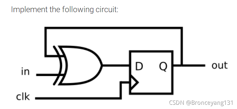
module top_module (
    input clk,
    input in,
    output reg out);

    always @(posedge clk)begin
        out<=in^out;
    end
endmodule
11. Mux and DFF
module top_module (
	input clk,
	input L,
	input r_in,
	input q_in,
	output reg Q);
  always@(posedge clk)begin
        if(L)begin
            Q <= r_in;
        end
        else begin
            Q <= q_in;
        end
  end
endmodule
12. Mux and DFF
module top_module (
    input clk,
    input w, R, E, L,
    output Q
);
always@(posedge clk)begin
        if(L)begin
            Q <= R;
        end
        else begin
            if(E)begin
                Q <= w;
            end
            else begin
                Q <= Q;
            end
        end
    end

endmodule
13. DFFs and gates
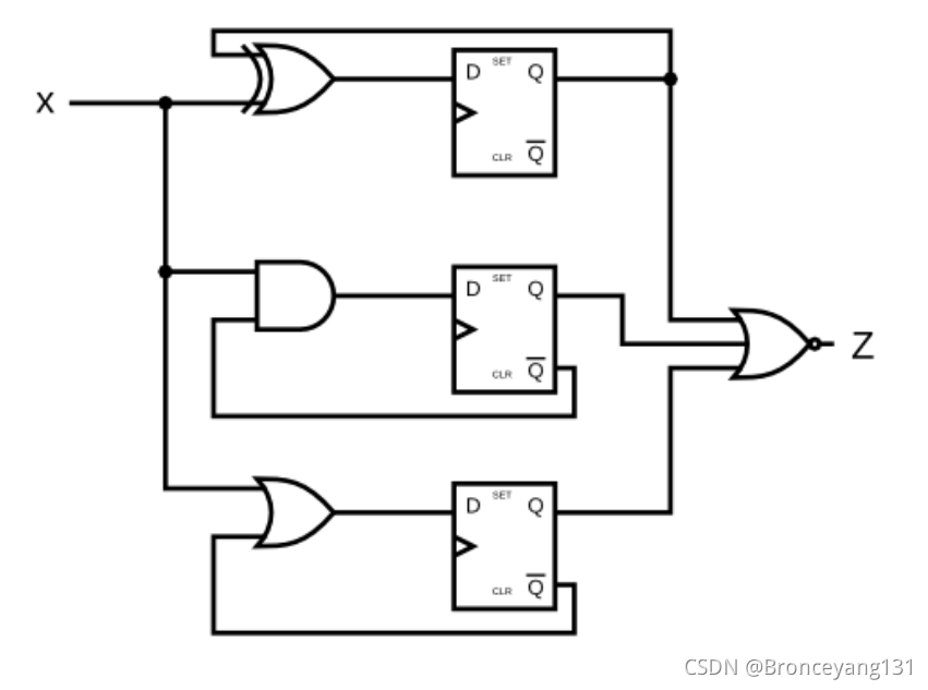
module top_module (
input clk,
input x,
output z
);
reg q1, q2, q3;
always@(posedge clk) begin
q1 <= q1 ^ x;
q2 <= ~q2 & x;
q3 <= ~q3 | x;
end
assign z = ~(q1 | q2 | q3);
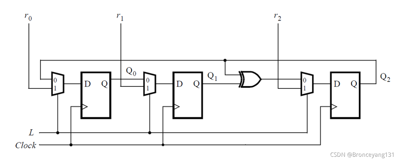
endmodule14. Create circuit from truth table
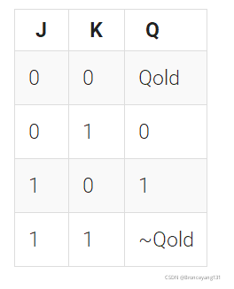
A JK flip-flop has the below truth table. Implement a JK flip-flop with only a D-type flip-flop and gates. Note: Qold is the output of the D flip-flop before the positive clock edge.
module top_module (
    input clk,
    input j,
    input k,
    output Q);
    always @(posedge clk)begin
        case ({j,k})
            2'b00:Q<=Q;
            2'b01:Q<=1'b0;
            2'b10:Q<=1'b1;
            2'b11:Q<=~Q;
        endcase
    end

endmodule
15. Detect an edge
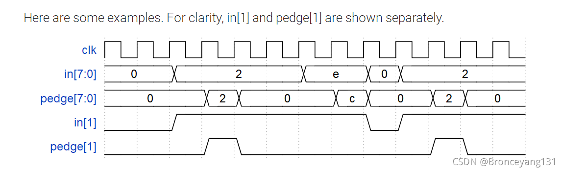
For each bit in an 8-bit vector, detect when the input signal changes from 0 in one clock cycle to 1 the next (similar to positive edge detection). The output bit should be set the cycle after a 0 to 1 transition occurs.
类似上升沿检测电路。
module top_module (
    input clk,
    input [7:0] in,
    output reg [7:0] pedge
);

    reg [7:0] in_delay;

    always @(posedge clk)begin
  		in_delay<=in;
    end

    integer  i;
	always @(posedge clk)begin
        for (i=0;i<8;i=i+1) begin
            if({in_delay[i],in[i]}==2'b01)
                pedge[i]<=1'b1;
             else
                 pedge[i]<=1'b0;
        end
    end
endmodule
16. Detect both edges
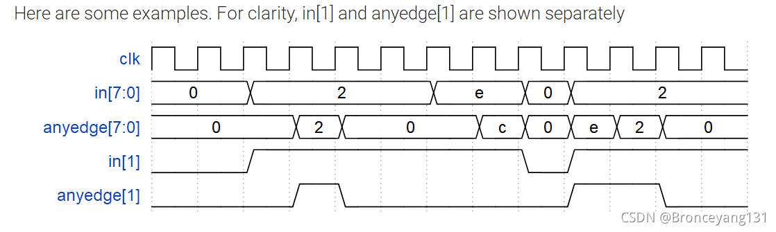
For each bit in an 8-bit vector, detect when the input signal changes from one clock cycle to the next (detect any edge). The output bit should be set the cycle after a 0 to 1 transition occurs.
module top_module (
    input clk,
    input [7:0] in,
    output [7:0] anyedge
);
    reg [7:0]in_delay;

    always @(posedge clk)begin
        in_delay<=in;
    end

    integer i;
    always @(posedge clk)begin
        for (i=0;i<8;i=i+1)begin
            if(in_delay[i]^in[i])
                anyedge[i]<=1'b1;
            else
                anyedge[i]<=1'b0;
        end
    end


endmodule
17. Edge capture register
For each bit in a 32-bit vector, capture when the input signal changes from 1 in one clock cycle to 0 the next. "Capture" means that the output will remain 1 until the register is reset (synchronous reset).
Each output bit behaves like a SR flip-flop: The output bit should be set (to 1) the cycle after a 1 to 0 transition occurs. The output bit should be reset (to 0) at the positive clock edge when reset is high. If both of the above events occur at the same time, reset has precedence. In the last 4 cycles of the example waveform below, the 'reset' event occurs one cycle earlier than the 'set' event, so there is no conflict here.
In the example waveform below, reset, in[1] and out[1] are shown again separately for clarity.

module top_module (
    input clk,
    input reset,
    input [31:0] in,
    output [31:0] out
);
    reg [31:0]in_delay;
    integer i;
    always @(posedge clk)begin
        in_delay<=in;
    end
     always @(posedge clk)begin
         if(reset)begin
             out<=32'd0;
         end
         else begin
             for (i=0;i<32;i=i+1)  begin
                 if({in_delay[i],in[i]}==2'b10)
                     out[i]<=1'b1;
             end
      end
  end
endmodule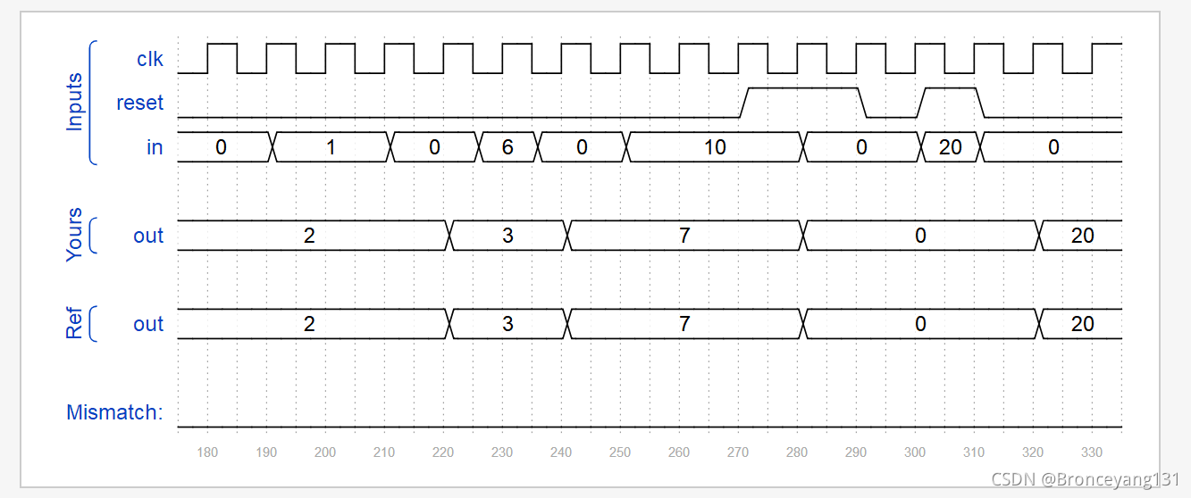
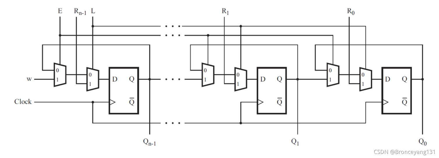
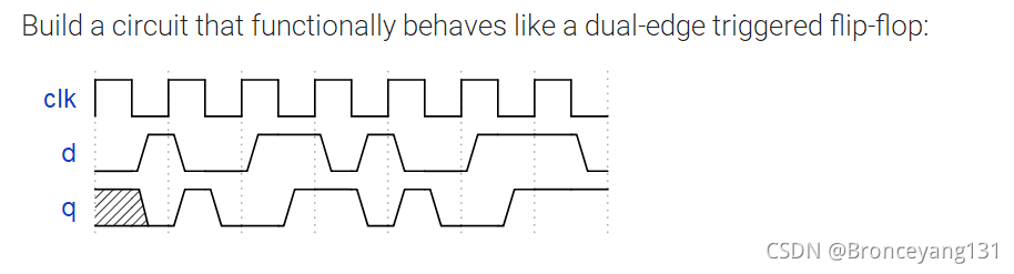
18. Dual-edge triggered flip-flop
双边沿采集数据或信号
You're familiar with flip-flops that are triggered on the positive edge of the clock, or negative edge of the clock. A dual-edge triggered flip-flop is triggered on both edges of the clock. However, FPGAs don't have dual-edge triggered flip-flops, and always @(posedge clk or negedge clk) is not accepted as a legal sensitivity list.
module top_module (
    input clk,
    input d,
    output q
);

  reg q1,q2;
    always @(posedge clk)
        begin
            q1 <= d;
        end
    always @(negedge clk)
        begin
            q2 <= d;
        end

    assign q = clk? q1:q2;

endmodule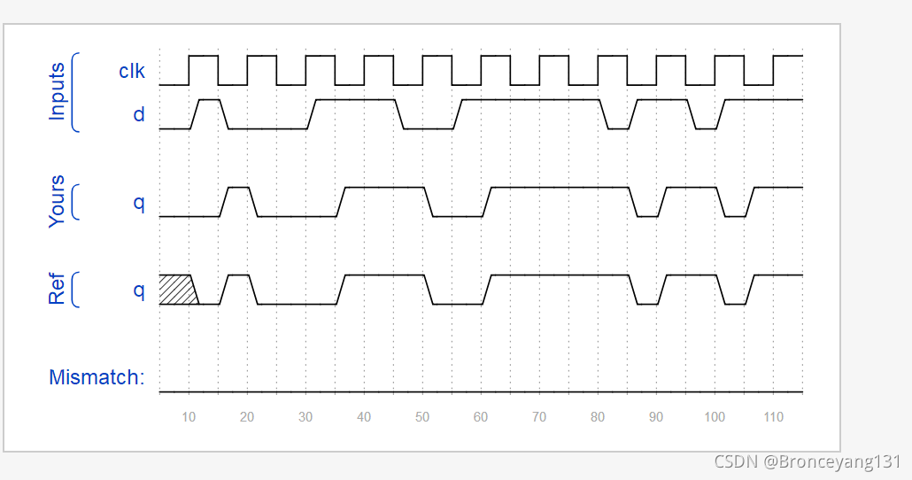


 491
491

 被折叠的 条评论
为什么被折叠?
被折叠的 条评论
为什么被折叠?
 到【灌水乐园】发言


