


 本文介绍了NAND和NOR门的通用性质,它们可以用来实现各种逻辑操作。通过使用双重符号(NAND和负或门符号),设计者能更直观地构建逻辑电路,如AND、OR、NOT等,而无需复杂的布尔代数计算。
Up to this point, you have studied combinational circuits implemented with AND gates, OR gates, and inverters.
In this section, the universal property of the NAND gate and the NOR gate is discussed.
The universality of the NAND gate means that it can be used as an inverter and that combinations of NAND gates can be used to implement the AND, OR, and NOR operations.
Similarly, the NOR gate can be used to implement the inverter (NOT), AND, OR, and NAND operations.
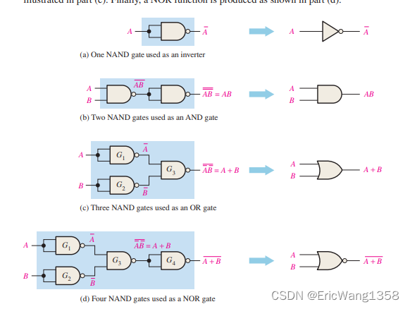
The NAND Gate as a Universal Logic Element
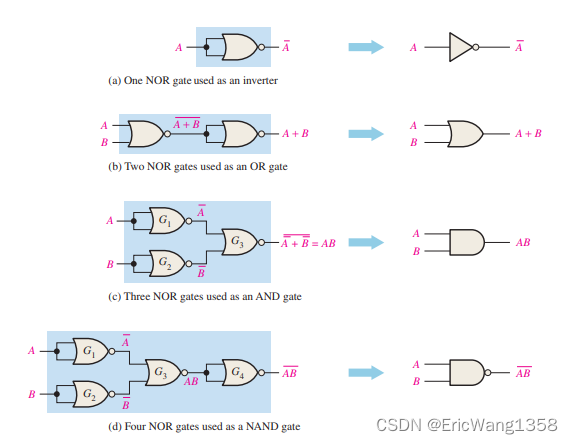
The NOR Gate as a Universal Logic Element
5–4 Combinational Logic Using NAND and NOR Gates
NAND Logic Diagrams Using Dual Symbols
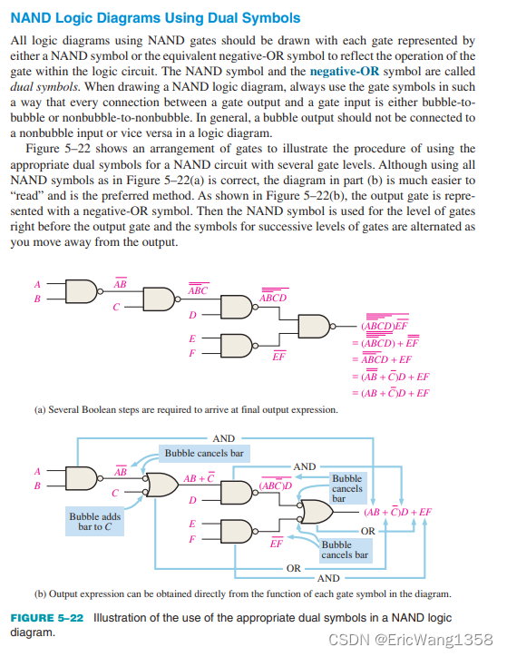
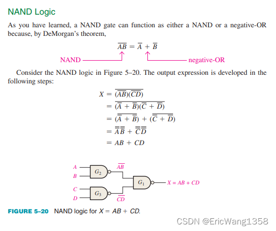
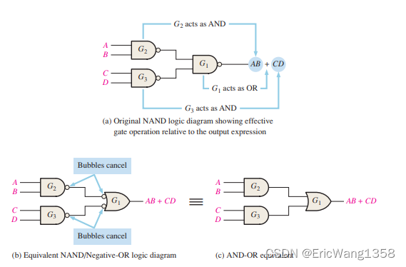
这张图展示了在NAND逻辑电路图中如何使用双重符号。所有的NAND逻辑图都应该使用NAND符号来表示每个门的逻辑功能,且与之相对应的是负或门(negative-OR gate)符号,这两种符号被称为双重符号(dual symbols)。在绘制NAND逻辑图时,应该以这样的方式使用门符号:每个连到门的输入端都是泡沫对泡沫(bubble-to-bubble)或者非泡沫对非泡沫(nonbubble-to-nonbubble)。通常,一个泡沫输出不应该连接到一个非泡沫输入,反之亦然。
图中的5-22展示了使用适当的NAND双重符号来组织门以说明这个过程。虽然图5-22(a)中所示的NAND符号是正确的,但图5-22(b)提供了一种更加容易“读取”的方法,而且是首选的方法。正如在5-22(b)中所示,输出门前的门是用负或门符号表示的,然后在输出前的级别使用NAND符号,随着你从输出移开,连续级别的门符号交替出现。
例如,下面解释一下图5-22中的两个部分如何工作:
(a) 部分:
- 输入A和B通过一个AND门,输出AB。
- 这个AB与C通过一个OR门,输出ABC。
- 然后,ABC与D通过一个AND门,输出ABCD。
- 接着,ABCD与E通过一个OR门,输出ABCDE。
- 最后,ABCDE与F通过一个AND门,得到最终输出ABCDEF。
这个过程需要通过多个布尔代数步骤来得到最终的输出表达式。
(b) 部分:
- 输入A和B通过一个AND门,同时C独立存在。
- A和B的AND门与C通过一个OR门,同时D独立存在。
- AB+C的结果与D通过一个AND门,同时E和F通过一个OR门。
- 最终,这两个结果通过一个AND门得到最终的表达式。
在(b)部分,你可以直接从每个门的功能和图中的符号得出输出表达式。这种方法不需要通过多步布尔代数运算,可以更直观地看到结果。
NOR Logic


 被折叠的 条评论
为什么被折叠?
被折叠的 条评论
为什么被折叠?
 到【灌水乐园】发言


