


1. Sigrity Power DC Simulation
1.1 PCB file prepare and load the .spd file to PDC
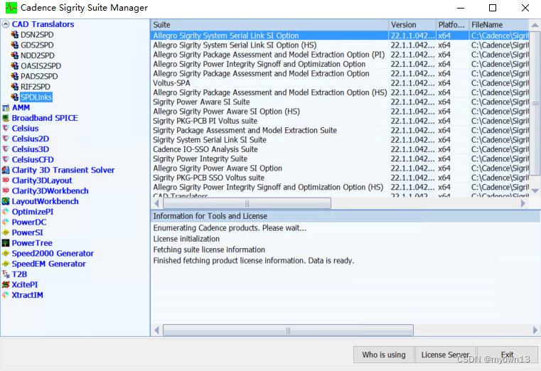
Step 1: Convert the .brd PCB board file to .spd file using the SPDLinks tools like below:
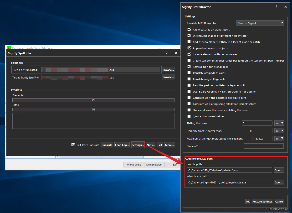
Step 2: Double click the Allegro Sigrity System Link SI option and we can see below .brd file to .spd file transfer link:
- Import the .brd file in the first File to be translated column;
- The .spd file will be auto generated in the Target Sigrity Spd File Column;
- Please check the Cadence extracta path setting if we can’t convert the .brd file to .spd file;
- Click the Translate and the file start to convert;
1.2 PCB stack-up && VIA check
We need prepare the PCB stack and Via plated copper(if we need consider the high temperature condition, we also need set the copper temperature coefficient detials for cover the high temperature case);
Step 1: Start the Power DC simulation engine and Load the .spd layout file:
Step 2: Materials model build up (This step can be skipped if we have already builded the material model and just re-use it directly.)
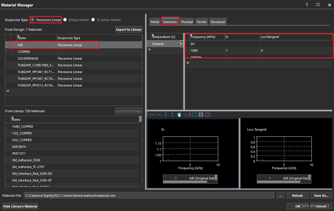
we usually need consier 4 types materials for the PCB stack-up setting: Air, Soldermask, Copper and Prepreg.
- Air: We need set the Dispersive type and **Dielectric ** relative parameters like below, and for extending the frequency range, we usually set the Frequency to DC, 1000MHz and Infinite. The Er of the Air is 1 (constant) and the loss tangent is 0;
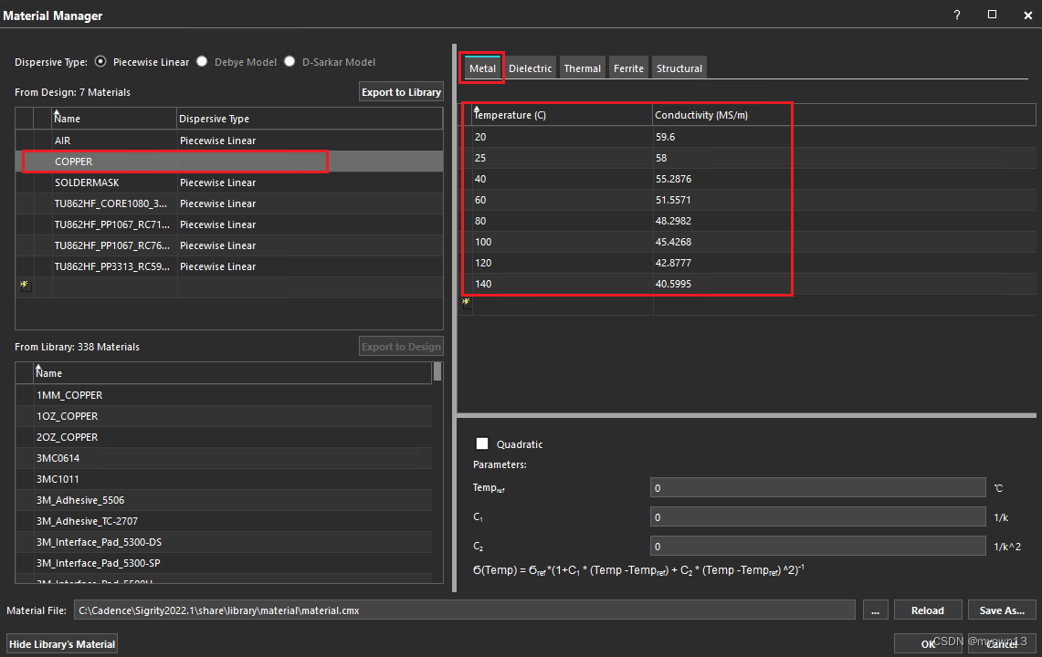
- Copper(current flow material): For the power DC simulation, since copper has the negtive conductivity coefficient (58MS/m for the 25C room temperature), need add the temperature realtive parameters like below:
Noted: The copper materials only need to set the Metal relative parameters.
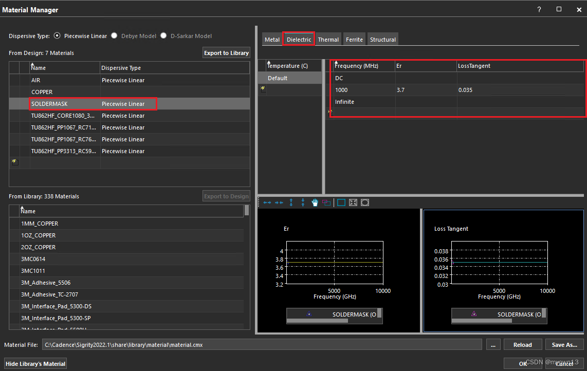
- Soldermask: PCB is usually covered by soldermask on top layer and bottom layer, so we need add the Soldermask Dielectric parameters for the power SI simulation, this value has no effect on Power DC simulation, but we still conver this topic here.
The typical dielectric parameters for the soldermask is shown as below (Dielectric constant is 3.7 and Loss Tangent is 0.0035 @1GHz);
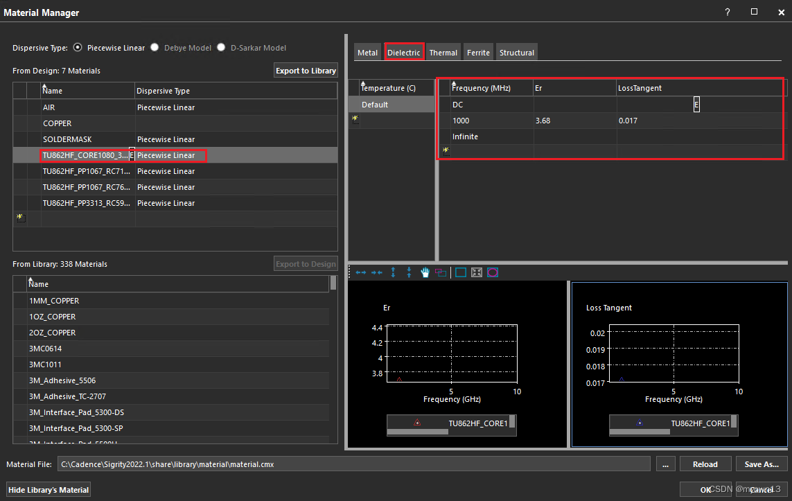
- Prepreg(Filled-in materials): Like the soldermask, the prepreg is very important for the high speed Power SI simulation, but almost has no effect on the power DC simulation, but we still cover the **Dielectric ** parameters settings here like below figure (Take the common used TU862HF prepreg_core_1080 as an example).
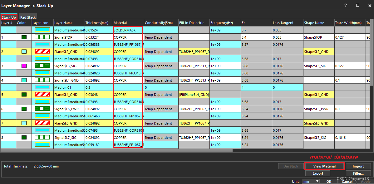
Step 3: PCB stack-up filled in: This step is mainly used for filling the materials from the database into the stack-up area;
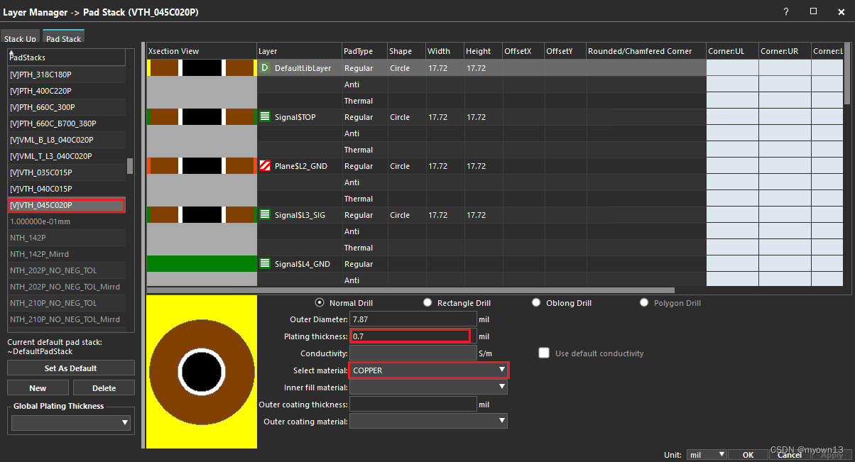
Step 4: Via padstack check – The purpose of this step is to fill copper into the PTH via or through hole for current flow;
Set the Via and PTH hole like below (Noted, the plated thickness is usually using the 0.7mil per the IPC spec(worst case))
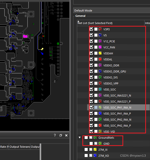
1.3 Set up P/G nets
Need check all the used power nets && GND nets and separate the nets into the Power && GROUND nets group.
1.4 Simulation environment setting check – temperature
Using the setting options, and set the ambient temperature to 85 degree if we want to cover the 85C usage case (Default temperature is 25C).
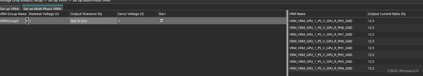
1.5 Set up VRMs
Noted: For the multi-phase buck DC/DC, we need use the same sense point(including the postive node and negtive node), then the multi-phase group will shows up like below (phases buck DC/DC power supply)
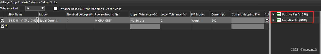
1.6 Set up Sinks
Usually use a current souce (like 240A current) with multi-node as the sinks.
1.7 Set up Discrete
First, if we want to add the Discrete between two nets, we need place the relative two nets into PowerNets or GroundNets.
1.8 Set up Ref Node
Choose the node (GND node) that you want to set as an Ref Node and right click on the node, then choose Set as Reference Node.


 2万+
2万+

 被折叠的 条评论
为什么被折叠?
被折叠的 条评论
为什么被折叠?
 到【灌水乐园】发言


