


Proc. IEEE 1994 Int. Conference on Microelectronic Test Structures, Vol7, March 1994
来自国际电子与电气工程师协会1994年关于微电子测试结构的会议,卷7,1994年3月
Modeling of Test Structures for Efficient Online Defect Monitoring Using a Digital Tester
使用一个数字测试仪进行高效率在线缺陷监控测试结构的模型
Christopher Hess, Larg H. Weiland
作者
Institute of Computer Design and Fault Tolerance (Prof. Dr. D. Schmid)
University of Karlsruhe, P.O. Box 6980, D-76128 Karlsruhe, Germany
Abstract - A novel methodology for digital measuring
procedures and digital data analysis is presented in order to
evaluate an online process control and defect monitoring. That
can be done by manufacturing test chips side by side with
standard chips and measuring them with the same measuring
equipment - the digital tester. To achieve a fast and effective
(efficient) measuring procedure and data analysis test structures
will be modeled in geometry-graphs, neighborhood-graphs and
connection-graphs.
抽象的 - 根据评估一二在线过程更控制和错误监控的为数字测量过程和数字数据分析的一个新的方法学被推出。它能够通过制造与标准
芯片同样规格的标准芯片和使用同样的测量设备-数字测试仪测量它们来完成。测试结构使用几何图形,领域图形,和连接图形来模型化,进行快速高效的测量过程和数据分析。
1 INTRODUCTION
1 介绍
Continuous data about process specific defect parameters like
the density of short circuits and open circuits are required for
yield prediction, design rule development, test pattern
generation and process problem debugging [Walk87], [Maly87],
[Spie93], [Mitc85], [LYWM86]. To determine significant data
of these parameters, test structures are used in separate lots
[Spen83]. An online defect parameter monitoring requires the
manufacturing of test chips side by side with standard chips so
that it is reasonable to use the same measuring equipment - a
digital tester with a standard probe card. Therefore, the test
structures will be embedded inside a regular boundary pad
frame.
像短的回路和开放回路的密度这样的过程特定缺陷参数的持续性数据对于产生预测,设计规则的开发,测试样式的生产和过程问题的调试时背需求的【沃克87】,【玛丽87】,【期刊93】,【Mitc85】,【LYWM86】. 确定测试这些参数的重要数据,测试结构在个别的选择中使用[Spen83]。一个显现缺陷参数监控系统为了使用同样的测试设备(使用同样探测卡的标准测试设备)需要同时生产测试板和标准板
, 这个测试结构会被嵌入一个规则范围的基片框架。
The evaluation with a digital tester requires a special measuring
procedure (see section 2). To achieve an effective data analysis,
novel test structure models have been developed which are
described in section 3. Section 4 shows the novel approach of
defect diagnosis and analysis. Section 5 gives some
experimental results.
使用数字测试仪的估算需要特定的测量过程(看第二节)。完成一个有效的数据分析,为完成有效的数据分析的新的测试模型的已经被开发,它将在第三节做描述。第四节展示新的错误诊断和分析的近似值。第五节给出了一些实验性的结果。
2 MEASURINPGR PROCEDURE USING A DIGITAL TESTER
数字分析仪的测量流程
In this section, two of the most common defects are discussed,
namely extra material defects and missing material defects.
Depending on whether the damaged material is conducting or
nonconducting, the defect can cause a short circuit fault or an
open circuit fault. In order to detect defects of these types,
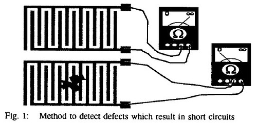
special test structures were developed. Comb structures (cf.
figure 1) [Bueh83] [LYWM86] [Walk871 aim at extra material
defects. These defects can cause a short between isolated lines
(usually designed as combs) and thus significantly reduce the
resistance measured between the pads.
在这个部分,讨论两个常见的缺陷,即附加材料缺陷和缺少材料缺陷。基于被损坏的材料是否在传导,这个缺陷能够导致一个短路错误或者开路错误。根据这种类型缺陷的检测,特定的测试结构被开发。梳理结构以额外的材料缺陷为目标(参考图1)【Bueh 83】【LYWM86】【Walk87】,这些缺陷能够在两个独立的线间导致短路(通常被设计作为梳理结构),因此两个基片间的电阻被显著地减少。
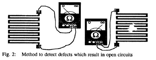
Meandering strings (cf. figure 2) [Bueh83] [LYWM86]
[Walk871 are applied to detect missing material defects. If these
defects are large enough, they interrupt the connection between
the pads and increase the measured resistance very much.
图1 : 检测短路缺陷的方法
曲线(参考图2)[Bueh83] [LYWM86][Walk871被应用到检测缺少材料缺陷。如果这些缺陷足够大,他们中断了两个基片之间的连接和增大了非常多的测量电阻。
To measure the resistance of a test structure, commonly analog
testers with a measurement frequency below 1 Hz are applied
[BCKJ91] [MiFH92] [RoBF92]. In the context of this paper, an
electrical test must only decide whether there is a defect or not.
So in general a digital tester should be sufficient.
图2:检测断路缺陷的方法
通常1Hz以下的模拟测试仪会被用来测量测试结构的电阻率[BCKJ91] [MiFH92] [RoBF92]. 。在这养的背景下,电子测试仪必须仅仅判断是否有一个缺陷。因此通常一个数字测试仪就够了。
A digital tester has important advantages. First, the
measurement frequency of a digital tester is normally many
times higher than the frequency that is possible with analog 2-
or 4-point measurements. So the evaluation of test structures
can be much faster. Secondly, every measured value needs only
one bit. This reduces the storage requirements. Thirdly, a data
reduction is possible already during the electrical measurements
since the measured binary data can easily be compared to
reference values. Finally, using a digital tester simplifies online
process control because test chips and standard chips can be
measured in the same way and with the same measuring
equipment.
电子测试仪有重要的好处。首先,电子测试仪正常比可能是模拟2-4点的测量频率高出很多。因此,测试结构的效率会非常快。第二,每个测量值需要仅仅一位。这缩小了存贮量需求。第三,因为测量的二进制数据能够容易的和参考值比较,在电子设备测量期间数字减少时可能的。因为测试片和标准片能使用同样的办法和同样的测量设备进行测量,使用数字测试仪简化了在线流程控制。
The results of feasible have shown that applying a digital
tester is feasible. The resistance values of about 100 equally
designed meandrous structures have been measured. In the
histogram of figure 3 two clusters can be distinguished clearly.
One of these clusters contains the resistance values of the fault
free meandrous structures. The other cluster is due to the
meandrous structures with defects causing open circuit faults.
In [MiFH92] a similar distribution was obtained.
可行的结果已经展示应用一个数字测试仪是可行的。大约等于100的被设计的迂回曲折结构的电阻值已经被测量。图3的两簇柱状图能够被清晰地辨别。这些簇中的一个包含无效的自由的回转的结构的电阻值。另一个被用作断路无效的缺陷原因的回转结构。在一个类似【MiFH92】的位置被包含。
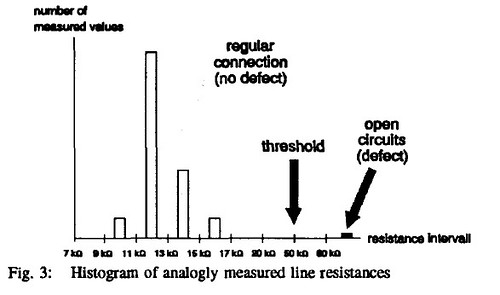
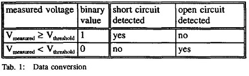
Using Ohm's law the resistance measurement can be reduced to
a voltage measurement. The threshold voltage of the digital
tester is set to a value in the middle between the two clusters
of figure 3. The two distinguishable intervals will be assigned
to the information "defect detected" or "no defect detected".
图3. 模拟测量电阻的线性柱状图
使用欧姆定律,电阻测量能够被换算成电压测量。数字测试仪的临界电压被设置成图3的两簇之间的一个值。两个可区别的区间会分别分配给信息缺陷检测或者无缺陷检测。
To achieve a complete adaption of a digital tester to the test
structure conditions, the stimulus Voltage V, and the measuring
frequency f,,, have to be adjusted too. [HeWe92] validates this
procedure for a checkerboard test structure.
表1. 数据转换
为了测试条件完成完整的数字分析仪的调整,激励电压V,测量频率f,,,不得不也被调整。【HeWe92】 验证了这个棋盘格式的测试结构。
3. Modeling of Test Structure
To enable an efficient analysis of digitally measured data, a
formal model of a test structure is introduced first. [CaDJ89]
describes a defect-graph modeling for analogly measured test
structures data, but this model only deals with short circuit
defects. An effective application to digitally measured data of
open and short circuit defects requires a novel comprehensive
methodology which will be described here.
3. 测试结构的模型化
为了能够进行高效率的数字测量数据的分析,一个正规的测试结构的模型首先被介绍。【CaDJ89】描述了一个模拟测量测试结构数据的缺陷图模型,但是这个模型仅仅完成了短路缺陷。一个高效率的开率和短路缺陷的数字测量数据的应用会在这里描述。
3. 1 Geometry-Graph of Test Structures
To realize an efficient digital data analysis, it is necessary to
model the geometry of layout objects inside a test chip with a
geometry-graph. The nodes stand for the measuring points and
the edges represent all conductive layout objects (conductive
component (cc)) like a comb or a meandrous line between two
measuring points. Conductive components, which are only
connected to one measuring point will be modeled as loops.
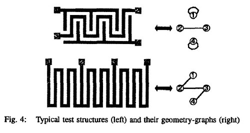
Figure 4 shows on the left side typical test structures [Bueh83],
LYWM861, [Walk871 and on the right side their geometrygraphs.
3.1 测试结构的几何图
为了实现高效的数据分析,使用几何图模型化一个测试片的结构图的几何结构是必须的。测量点和边界的节点处描述了所有像在两个测量点之间的梳子或者啊一条迂回曲折的线一样的传导结构图(传导的组成部分)。传导的组成部分仅仅连接一个作为回路的被模型化了的测量点。图4左边展示了典型的测试结构【Bueh83】,LYWM861,【Walk871,在右边展示了它们的几何图。
Measuring points which are accessible for the measuring
equipment are equal to the pads of a test chip (and therefore
also called pads). All not accessible measuring points are called
internal nodes. To implement internal nodes in a test structure
design is up to the designer, but it shouldn't be forgotten that
internal nodes can cause irreversible defect and fault coverage
problems [Bueh83] [Hewe931 [Guga931.
图4. 左边是典型的测试结构,右边是它们的几何图
对已测试设备来说比较容易接近测量点等于测试板的基片(因此也称作基片)。所有不可接近的测量点叫做内部点。对设计者来说完成测试结构设计的内容节点,内部节点能导致不可挽回的错误和无效覆盖问题不应该被忘记。
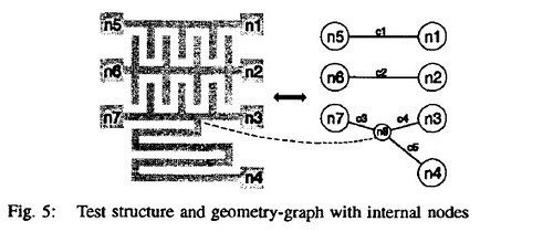
图5. 内部节点的测试结构和几何图
3.2 Neighborhood-Graph of Test Structures
The identification and localization of short circuit defects
require also information about the neighborhood relationship
between differently connected layout objects [Hest931
[HeWeWa]. Generally a test structure contains a set of
conductive components (conductive layout objects) which are
possibly arranged in different layers. A maximal set of
conductive components and measuring points that are
connected to each other is called a maximal conductive
component (mcc). Each mcc should contain at least one pad.
3.2 测试结构的邻域图
短路缺陷的标记和位置也需要关于在不同连接的设计图之间邻域关系的信息【Hest931 【HeWeWa】。通常一个测试结构包含一套可能分布在不同层次的传导部件(传导设计图)。一套最大的传导部件和测试点互相连接被称为最大传导部件。每个最大传导部件至少包含一个基片。
The neighborhood relationship of mcc's inside the whole test
structure is modeled by the neighborhood-graph (mccn-graph).
The nodes represent the maximal conductive components of the
fault-free test structure. So every node of the neighborhoodgraph
corresponds to a subset of pads (=nodes of the geometrygraph)
and conductive components (=edges of the geometrygraph)
which belongs to one single mcc. Two nodes mcc,,
mcc2 are connected by an edge if and only if in some region of
the test structure a layout object of mcc, and a layout object of
mccz lie side by side or one on top of the other with only
nonconducting material between them. Thus the edges
correspond to shorts that can be caused by defects (undesigned
shorts). Figure 6 shows typical test structures and their
neighborhood-graphs. To refer to the geometry-graph the mcc
index of one node in the neighbor-hood-graph contains the
indices of all pads (=nodes inside the geometry-graph) which
belongs to this specific mcc.
在整个测试结构里德最大传导部件的邻域关系被邻域图模型化(最大传导部件邻域图)。节点描述的是最大无故障测试结构的最大传导部件。因此每个邻域图的节点相当于一个基片的子集(几何图的节点)和属于一个单独最大传导部件的传导部件(几何图的边线)。两个节点最大传导部件如果仅仅如果一个最大传导部件的设计图在一个测试结构的某个区域里被边线连接,最大传导部件的设计图一个挨一个或者当使用绝缘材料连接时一个在其他的顶部。因此边线相当于能够被缺陷(未设计的短路)导致的短路。图6展示了典型的测试结构和他们的邻域图。参考属于特定最大传导部件的包含所有基片(在几何图里的节点)的指数的邻域图里的一个节点的索引的几何图形。
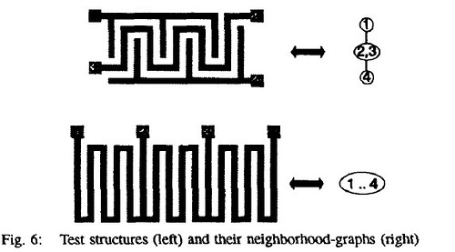
图6. 左边是测试结构,右边是他们的邻域图
In [CaDJ89] the defect-graph has been defined for a similar
purpose. Its nodes have the same meaning as in the
neighborhood-graph, but its edges describe only the undesigned
shorts that are considered in the measurement analysis. So the
defect-graph mixes information about the design of the test
structure (nodes) and information about the evaluation (edges).
In contrast, the structure of the neighborhood-graph introduced
above is determined solely by the geometric features of the test
structure. It is independent of the applied analysis procedure.
在[CaDJ89]缺陷图已经被定义了一个类似的目标。它的节点和邻域图有同样的意思,但是它的边线描述仅仅在测量分析中未设计的短路。因此缺陷图混合了关于测试结构(节点)和估算信息(边线)的设计的信息。对比,邻域图的结构介绍了上面的测试结构的几何图表的确认。它是和应用分析流程无关的。
3.3 Connection-Graph of Test Structures
An efficient measurement data management requires
information about the connections between the measuring
points (pads) of a test chip [HeWe92]. During the electrical
measurement a voltage can be measured between two pads of
a test chip. For that every test chip will be modeled with a
connection-gruph. Here, the nodes stand for the accessible
measuring points (pads) and the edges represent the conductive
connections (measurable current flow) between accessible
measuring points. The connection-graph of a fault-free test
structure is called golden device. Figure 7 shows on the left
side two test structures and on the right side their connectiongraphs.
3.3 测试结构的连接图
高效的测试数据管理需要关于在测量点(基片)和测试板(HeWe92)之间的连接的信息。在电子测量期间电压能够在测试板的两个基片之间被测量。因此每个测试板会被模型化成为连接图。这里,可接近的测量点(基片)的节点位置和边线描述了可接近测量点的传导连接(可度量的电流)。无故障测试结构的连接图被称为黄金设备。图7左边展示了两个测试结构,右边展示了他们的连接图。
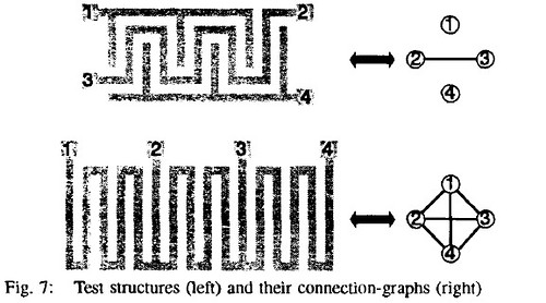
图7左边展示了两个测试结构,右边展示了他们的连接图。
4 DATA ANALYSIS
The measurement results of test structures are representable by
matrices, which can be converted into the graphs described
above. The detection of the defects will be achieved by
comparing the different graphs or their matrices, respectively.
This section therefore presents novel algorithms which enable
machine-assisted defect diagnostics.
4 数据分析
测试结构的测量结果可以用矩阵来描述, 也可以使用图表来描述。 缺陷检测会分别地通过比较不同的图或者他们的图表来完成。这节推出了能够使用机器辅助的缺陷检测的新算法。
The data of a digital tester are normally arranged in two
matrices. The test matrix (stimulus matrix) contains the test
vectors, where each row represents a test vector and the
columns represent the different stimulus points (pads). The
response matrix contains the measured vectors where each row
represents the measured response to a test vector and the
columns represent the different measuring points or pads
respectively. Normally bidirectional tester channels are used, so
that a test structure without any active elements (transistors,
diodes, ...) will be completely tested by using a "walking one"
as test vector set ("1" = channel in stimulus mode; "0 =
channel in response mode) over all pads. Figure 8 shows an
example of the described procedure for a test structure with 7
pads, where bidirectional tester channels are used with a
walking one in the stimulus matrix.
数字测试仪的数据正常地被安排在两个矩阵里面。测试矩阵(激励矩阵)包含测试向量,每行描述一个测试向量,列描述不同的激励点(基片)。响应矩阵包含每行表述的测量的响应到一个测量矩阵和列描述的不同的测量点或者基片的测量向量。通常双向的测试仪通道被使用,因此没有活动元素(晶体管,二极管,....)的测试结构会用“走一个”作为测试矩阵设置(1=激励模式通道,0=响应模式通道)在整个基片上进行完整的测试。图8展示一个描述了一个7个基片的测试结构的流程的例子,双向的测试仪信道在激励矩阵的走一个模式下被使用。
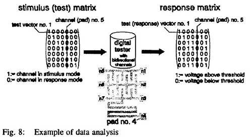
图8. 数据分析的例子
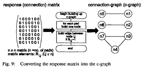
Each test vector and its measured response can be converted
into a connection-graph [HeWe93] [Guga93]. In case of using
a "walking-one'' the conversion into the connection-graph is
simplified, because the rows and columns of the quadratic
response matrix directly represent the accessible measuring
points (pads). A "1" in row i and column j stands for a
measured conductive connection between the node i and the
node j. A "0 in row i and column j stands for a measured
nonconductive connection between the node i and the node j.
The following figure shows the conversion algorithm.
每个测试向量和它的测量响应能够被转换成一个连接图。[HeWe93][Guga93]。使用一个“走一个”模式转换到连接图是简单的,因为二次方程式的行列响应矩阵直接描述了可接近的测量点(基片)。1位于行i和列j也就是在节点i和节点j之间的被测量的转换连接的位置。0位于行i和列j也就是在节点i和节点j之间的被测量的非转换连接的位置。下面的图片展示了连接算法。
A missing or extra connection can be concluded from the
comparison of the different graphs, which also leads to the
localization of resulted defect. Subsection 4.1 deals with the
detection of open circuits and subsection 4.2 describes the
method to detect short circuits. Both methods are explained by
an example. For that the following figure contains the fault free
test structure of figure 5 and all necessary graphs.
一个消失的或者额外的连接从不同图的比较能够被得到结论,它也能索引到缺陷的位置。4.1节给出了开出检测,4.2节描述了短路检测。两个方法都是通过例子被解释的。对这个来说下面的图包含了图5的无故障测试结构和所有必需的图。
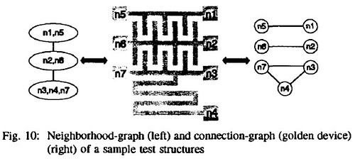
图10. 对于一个测试结构例子来说,左边是邻域图,右边是连接图(黄金设备)
For this example we assume that the structure has two different
defects as can be seen in the following figure.
对于这个例子来说我们猜想这个结构有两个不同的缺陷能够在下面的图中被看到
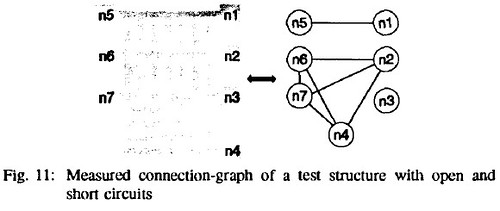
图11. 短路和断路的测量连接图
4.1 Open Circuits
The detection of open circuits requires a comparison of the
measured connection-graph to the geometry-graph of the test
structure. Due to the existence of internal nodes, the measured
connection-graph has to be transformed into a graph, which is
directly comparable to the geometry-graph. In the first step all
effects caused by short circuits have to be faded out. For that
the measured connection-graph will be compared with the
golden device. The AND operation (cf. table 2) of the edges of
these two graphs lead to the novel c-graph.
4.1 开路
开路检测需要这个测试结构连接图和几何图的比较。因为内部节点的存在,测量连接图不得不被转换成一个图形来直接和几何图比较。在第一步所有的被短路影响的效果不得不渐弱。对这个测量来说连接图会被用来和黄金设备进行比较。这两个图的边线的与操作(表2)带来了新的部件-图。
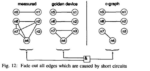
图12. 淡出所有的被短路导致的边线
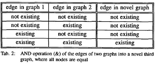
表2:两个图的边线的与操作形成了一个新的图,所有的节点都是相等的。
In the second step the c-graph has to be transformed into an
extended c-graph (ec-graph), which also includes intemal
nodes. For that each edge in the c-graph is replaced by the
equivalent path (including intemal nodes) of the geometrygraph
.Also, all edges get an index with reference to the
geometry-graph.
在第二步部件-图不得不被转换成一个扩展的部件图(扩展部件-图),它也包含了内部节点。对于在部件图中的每个边线被等价的几何图形路径(包括内部节点)。同样,所有的边线得到一个参照这个几何图形的索引。
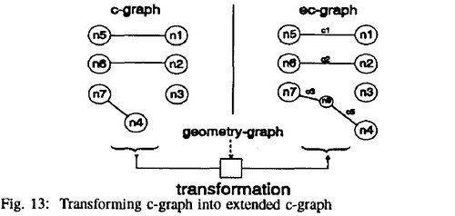
图13. 转换c图到扩展c图
Finally the ec-graph will be compared to the geometry-graph to identify open circuits.
For that a NOT operation (cf. table 3) will be applied to the edges of the ec-graph. Afterwards
an AND operation (cf.table2) of the edges of these two graphs lead to the result-graph. Each
edge in this result-graph represents an open circuit in the implemented conductive
component. In this example an open circuit in the conductive component "c4" was detected.
最终扩展部件图会在几何图到标记开路的比较。对于一个非操作(表3)会被用作ec图的边线。其后两个图的边线的与操作(表2)会带来结果图。在结果图里的每个边线描述了在已执行的传导部件的开路。在这个例子中在传导部件的"c4"开路被检测。
图14. 开路分析
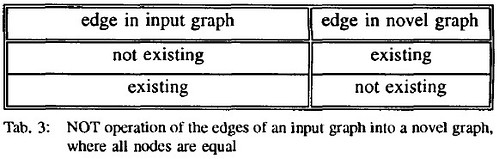
表3. 输入图形进入新图的边线的非操作,所有节点是相等的
The following figure shows the general methodology to detect
open circuits.
接着的图展示了开路检测的一般方法。
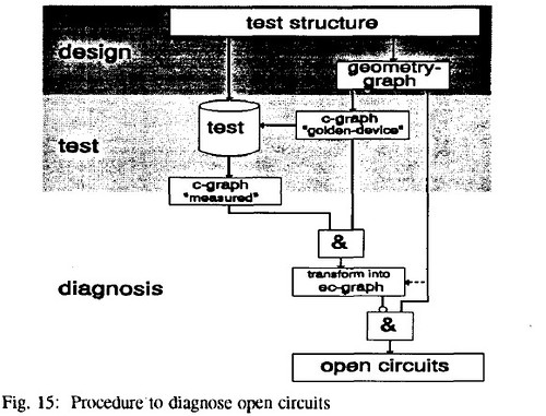
图15. 检测开路的程序
4.2 Short Circuits
The detection of short circuits requires a comparison of the
measured connection-graph to the neighborhood-graph of the
test structure. Due to the existence of multiple pads at one
single mcc, the measured connection-graph has to be
transformed into a graph which is directly comparable to the
neighborhood-graph. In the first step all designed connections
have to be faded out. For that a NOT operation (cf. table 3)
will be applied to the edges of the golden device. Afterwards
an AND operation (cf. table 2) of the edges of these two
graphs lead to the novel c-graph.
4.2 短路
短路检测需要被测量的连接图到测试结构的邻域图的比较。因为在一个单独的最大传导部件的多基片的存在,被测量的连接图不得不被转换成
直接和邻域图比较的图形。在第一步所有被设计的连接不得不被淡出。非操作(表3)会被应用到黄金设备的边线。在那之后,两个图的边线的与操作(看表2)带来了新的c图。
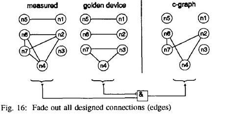
图16. 淡出被设计的所有设计的连接(边线)
In the second step the c-graph has to be transformed into a
mcc-graph, which only includes all maximal conductive
components as nodes (of the mccn-graph). For that every subset
of pads (=nodes of the c-graph) and conductive components
(=edges of the c-graph), which belongs to one single mcc will
be summarized to one node in the mcc-graph. Multiple edges
between two nodes of the novel mcc-graph will be replaced by
one single edge.
在第二步组成图不得不被转换成最大传导组成图,它仅仅包含了所有作为节点的最大的传导部件(最大传导部件节点图)。对于每个基片的子集(=部件图的节点)和传导部件(部件图的边线),它们属于一个单独的最大传导部件,它们会被总结成一个在最大传导部件的节点。新的最大传导部件的两个节点之间的多边线会被一个单独的边线代替。
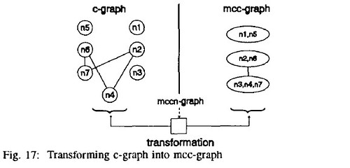
图17. 转换部件图到最大传导部件图
Finally the mcc-graph will be compared to the mccn-graph to
identify short circuits. The AND operation (cf. table 2) of the
edges of these two graphs lead to the result-graph. Each edge
in this result-graph represents a short circuit between different
mcc’s. In this example a short circuit between mcc(n2,n6) and
mcc(n3,n4, n7) as determined.
最后最大传导部件图会和最大传导部件节点图比较短路标记。两个图的边线的与操作(看表2)带来了结果图。结果图的每个边线描述了不同最大传导部件的不同。此例中在最大传导部件(n2,n6)和(n3,n4,n7)之间的短路被检测。
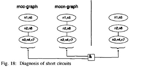
图18. 短路检测
The following figure shows the general methodology to detect
short circuits.
下面的图展示了检测短路的一般方法
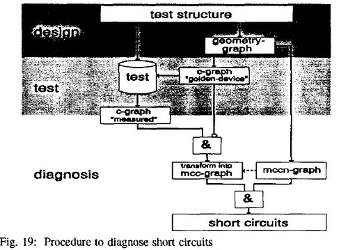
图19. 检测短路的流程
4.3 Machine Assisted Data Analysis
Both methods to detect defects are independently applicable.
For that the comparison and transformation of the graphs are
transferable into computer algorithms [Hewe931 [Guga93].
This methodology of data handling is included in a program
called VIADUCT (Versatile Automatic Identification Analysis
of Defects from Undesigned Open and Short Circuits in Test
Structures).
4.3 机器协助数据分析
检测缺陷的两个方法是独立的适当的。对于这两个方法来说图像的比较和转换是转换为计算机算法。【Hew931【Guga93】。这个数据控制的方法被包含在叫做VIADUCT(在测试结构里的未定义的开路和闭路的缺陷的多功能自动化标记分析)程序里
5 EXPERIMENTAL RESULTS
Nearly l000 test chips with different test structure designs were
manufactured at the Instirutfir Mikroelektronik Stuttgart (IMS)
to validate this procedure of data measurement and analysis.
To detect open circuit defects, 20 meandrous lines were
designed in a single metal layer inside a boundary pad frame of
40 pads.
5. 实验性的结果
不同测试结构设计的大约1000个测试板在斯图加特研究院被生产来验证这个数据测量和分析的流程。为检测开路缺陷,20个环线被设计在一个40片基片的分界线基片框架里德一个单独的金属层。
To detect short circuits, 20 comb lines were also designed in a single metal
layer inside the same boundary pad frame. All in all 9 modules per test chips
with different line width and space were implemented. These chips were
measured first with a digital tester and later on with an analog tester. Both test
methods yield the same number of detected defects. The figures
20 and 21 contain the comparison between digitally and
analogly detected defects.
为检测短路,20个梳理线也被设计在同样分界基片框架里德单独的金属层。不同线宽和距离的每个测试板
所有9个模块的梳理线被执行。这些板首先被一个数字测试仪测量,接着被一个模拟测试仪测量。两个测试方法
产生了同样的检测错误的数字。图21和22包含了在数字和模拟检测缺陷的比较。
图20. 模拟测量和数字测量短路缺陷的比较
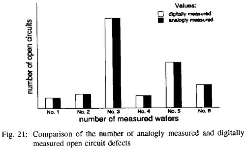
图21. 物理测量和数字测量开路缺陷的比较
The difference of measuring time was 2*10(e-3) seconds per test
chip for the digital test and 20 seconds per test chip for the
analog test. Furthermore all analogly measured data have to be
stored and analyzed, because a data comparison with reference
data during the electrical measurement is impossible.
测量时间的不同是数字测量每片的时间是 2*10(e-3)秒,模拟测试每片测试时间是20秒。而且所有的模拟测量数据不得不被存贮和分析,因为在电子测量期间的参考数据的数据比较是不可能的。
Due to the easy data comparison between digitally measured
data and their reference data an effective data reduction is
already achieved during the electrical measurement. Only the
data which differ from the reference data have to be stored and
analyzed. So the analysis of the digital test chip data takes less
time than the analysis of the analogly measured data.
因此在数字测量数据和他们的参考数据容易的数据比较,在电子测量期间有效的数据减少已经完成。仅仅和参考数据有差异的数据不得不被存贮和分析。因此数字测试片数据的分析比模拟测试数据的分析花费更少的时间。
Using the program VIADUCT on a Sun4 workstation, the data
analysis time was less than 1 sec per module.
在Sun4工作站使用程序VIADUCT,数据分析时间每个模块小于1秒。
Figure 22 shows some results of the additional optical defect
inspection.
图22 展示了附加的光学的缺陷检测结果
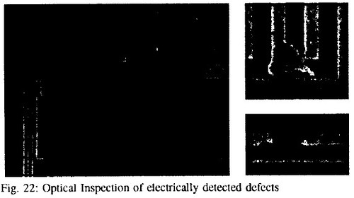
图22. 电子检测缺陷的光学检测
6 CONCLUSION
The accuracy of defect detection using a digital tester is the
same as the accuracy of most common analog measuring
procedures, but the measuring time is at least l0000 times
faster. This is important if checkerboard test structures
[HeWe92] [Hess931 [Hest931 are used because the number of
2 point measurements is too high for an efficient analog
measurement. The comparability of digitally measured data and
the usage of the described test structure graph models leads to
a faster data analysis. Finally, the usage of a digital tester
simplifies an online process control, because test chips and
standard chips can be measured in the same way with the same
measuring equipment.
6. 结论
使用数字分析仪的缺陷检测的精确性事同样的和最普通的模拟测量过程的精确性,但是测量时间至少快10000次。这事重要的,如果棋盘结构的测试结构,因为2点测量对于一个高效的模拟测量来说太高了。数字测量数据的比较和被描述的测试结构图模型的使用带来了快速的数据分析。最后,数字分析仪的使用简化了在线流程控制,因为测试板和标准版能够使用同样的测量设备和测试办法来测量。
ACKNOWLEDGMENT
This research was supported by Drutsche Forschungsgemeinschuft
(DFG), Schm 623/3-1. The authors thank Dr. H.
Richter and B. Laquai (Institut fur Mikroelektronik Stuttgart)
for advice and assistance with testing procedures. We also
thank Dr. A. Strole (Institut fur Rechnerentwurf und
Fehlertoleranz) for his cooperation, encouragement and helpful
discussions and A. Gugau for his activities in the
implementation of the program system VIADUCT.
鸣谢
这个研究被 Drutsche Forschungsgemeinschuft
(DFG), Schm 623/3-1支持。作者感谢 H.
Richter和 B. Laquai先生(fur Mikroelektronik Stuttgart学院)在测试流程的建议和帮助。也感谢A. Strole 先生的协作,鼓励和有帮助的讨论。感谢A.Gugau先生在程序系统VIADUCT的执行活动。
[BCIWII
[UuehX3I
[CaDJXY]
[Guga93]
[€1ess93]
[ HeStY 31
[Hewe921
[HeWe93]
[IleWe94a]
[LYWMX6]
[Maly87]
[ MiFI I Y 21
[ Mitc85j
[ RoU "21
[SpmR3]
[Spie93]
[WalkX7]
REFERENCES
Bruls, E. M. J. G., Camenk F., Krelschman. €1. I., Jess. I. A C,. A
Gcnciic Melhixl tu Devclop A Defect Moriitonrig System fur IC Processes
Interiiatii~iid 'Test Conference, I'N I
Uuehler. M G
Microelectronic Test Chip5 for VLSI Electronics
VLSI Electruiiics Microstructure Science. Vol 0. Chap.9. Academic Press.
19x3
Cainerik, F. Dirks. P A. I , Jess. I. A. G
Qualiiicatiun and Quantification of Prwcsa-Inducted l?uduct-Related
Defect
IEEE liilernatiunal Teat Conference. lYX9
Gugau, A.
Bntwicklung eines modularen Progranunsyatems zur MelWatenaufhrreilung
Studienarhcit am Instilut fur Rechnerenlwurf und Fehlcrtuleranz,
lliiiversitbt Karlaruhe. Juli 1993
Iless, c.
Teslstruktureii zur elfizieiileii prirdukti,iiirheglcitenden Defektdiagnose und
-analyse
CME-Fauhhgung, Lhsden. 1993
Hess, C., Slrole. A.
Modeling of Real Defect Outlines for Defect Size Dialrihution and Yield
Prediction
lntemationd Conference on Microelectronic Test Structures. Barcelona.
Much 1993
tless, C.. Weiland. L. 11.
Test Structure for the Detection. lucalization, and Identilication of Short
Circuits with a fligh Sped Digital Teater
Inteniationd Conference on Micruelectrmic Test Structures. San Diego,
Mach 1992
1Ieaa. C . Wciland. L. I1
Mdcllicrung von Test/trukturen Lur effizienten pr~,duktlons~gleitcnden
Dcfektd~tcnanalyse mil Ililfe tines Digitaltcalcr/
Technirch wissenschdtlicher Bericht. lnstitut fur Rcchnerentwurf und
I'ehlentileranz. 1 Iniversildt Knrlsruhe. 1993
Iless. C , Weiland. L. I I
Drop in Proces, Control Checkerhxud Test Structure for Efficient Online
Prtxess Characterization wid Defect Prohlem Debugging
liitematiunal Conference 011 Micrwlectnmic Test Structures. San Diego,
I994
Luksszek. W.. Yuhruugh, W.. Wdker, T, Meindl 1.
CMOS Test Chip Deign for Prucrss Prohlcm %hugging and Yield
Prediction Expeninenls
Solid Slate Technology. Much 1986
Mdy. W
Realistic Fault Modeling for VLSI Testing
241h ACMnEEE Design Automation Conference. 19x7
Mitchell. M A.. Forner. L., Huang. I.
Issues with Contact Defect Test Structures
IEEE International Conference on Microelectronic Test Structures. San
Diego. 1992
Milchell. M. A
Defect Test Structures fur Characlerizatlon of VLSI Technologies
Solid Stale Technology, May 19x5
Rodriguez-Monta6bs. R ,BN~s. E. M J. G.. Figuera, I.
Uridgiiig TkfecLs Resistance Measurernenls in a CMOS Proces/
IEEE Internationd Test Conference, 1992
Spencer, R
Matallrwtion Test Structures fur Drop In Prinxss Monitors
Solid State Technulogy. Septernher 19x3
Spiegel, G
Optimized Test Cost Using Fault Pruhahilities
ETC 91. Pmis. April 1991
Walker. D. M €1
Yield Simulation for Integrated Circuits
Kluwcr Academic Publisher. Boston. 1987
被使用,


 2370
2370

 被折叠的 条评论
为什么被折叠?
被折叠的 条评论
为什么被折叠?
 到【灌水乐园】发言


