


基本知识
IIC: inter-integrated circuit bus ,即 集成电路总线,串行通信,多主从架构,半双工(对讲机),小数据量场合,短距离传输。
速率:100kb/s 、 400kb/s 、 3.4Mkb/s
传输单位:8位(一个字节)(双向)
架构:每个IIC器件都可作为主/从器件,一个时间只有一个主设备
两条总线线路:SCL(串行时钟线)、 SDA(串行数据线)总线拓扑结构如图
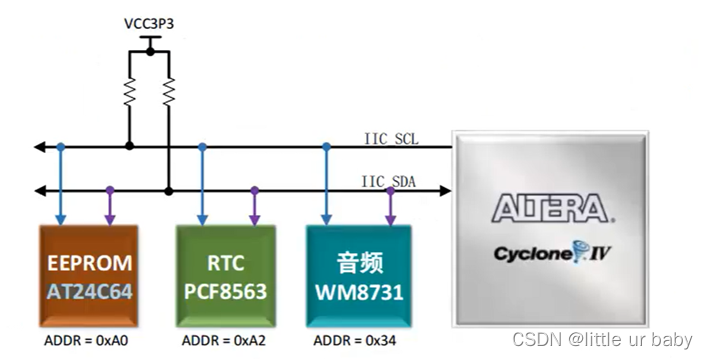
图中,每个IIC器件拥有唯一地址(识别码)。
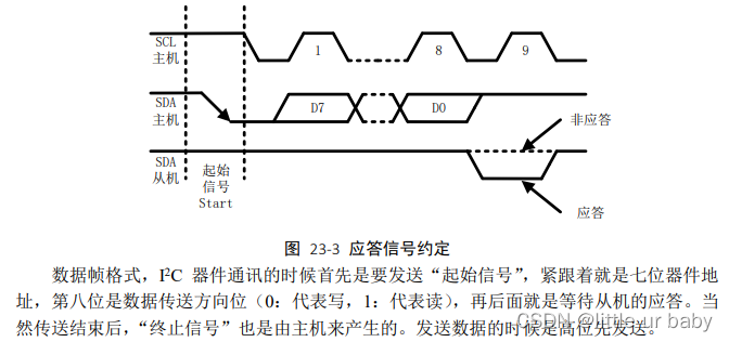
主机往总线上发送地址,所有的从机都能接收到主机发出的地址,然后每个从机都将主机发出的地址与自己的地址比较,如果匹配上了,这个从机就会向总线发出一个响应信号。主机收到响应信号后,开始向总线上发送数据,与这个从机的通讯就建立起来了。如果主机没有收到响应信号,则表示寻址失败。
IIC帧格式
默认规定:SCL高电平时,SDA稳定;SCL低电平时,SDA变化。(依此设定SDA的数据变化时刻,在SCL的低电平中点变化较为靠谱).在scl高电平时读/写数据。
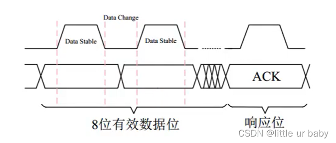
响应位:当 IIC 主机(不一定是发送端还是接受端)将8位数据或命令传出后, SDA释放,即设置为输入,然后等待从机应答(低电平 0 表示应答,1 表示非 应答),此时的时钟仍然是主机提供的。
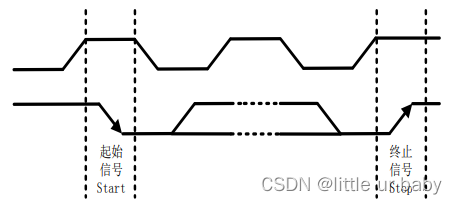
起始信号:SCL高且SDA出现下降沿。
停止信号:SCL高且SDA出现上升沿。
器件地址
每个I2C器件都有一个器件地址,有的器件地址在出厂时地址就设置好了,用户不可以 更改(例如 OV7670 器件地址为固定的 0x42),有的确定了几位,剩下几位由硬件确定(比 如常见的I2C接口的EEPROM存储器,留有3个控地址的引脚,由用户自己在硬件设计时确定)。
对于AT24C64这样一颗EEPROM器件,其器件地址为1010加3位的片选信号。3位片选信号由硬件连接设定。当硬件电路上分别将这三个引脚连接到 GND 或 VCC 时,就可以设置不同的片选地址。
I2C传输时,按照从高到低的位序进行传输。控制字节的最低位为读写控制位,当该位 为0时表示主机对从机进行写操作,当该位为1时表示主机对从机进行读操作。
在某些IIC器件中,A2 A1 A0可以当作存储单元地址来用。存储器地址一般为1或2字节。取决于IIC器件容量。
IIC写时序
时序:
1、主机设置 SDA 为输出;发送起始信号;
3、主机传输器件地址字节,其中最低位为 0,表明为写操作;
4、主机设置 SDA 为三态门输入,读取从机应答信号;
5、读取应答信号成功,主机设置 SDA 为输出,传输地址数据高字节;
6、主机设置 SDA 为三态门输入,读取从机应答信号;
7、读取应答信号成功,主机设置 SDA 为输出,传输地址数据低字节;
8、设置 SDA 为三态门输入,读取从机应答信号;
9、读取应答信号成功,主机设置 SDA 为输出,传输待写入的数据;
10、设置 SDA 为三态门输入,读取从机应答信号;
11、读取应答信号成功,主机产生 STOP 位,终止传输。
IIC页写时序(连续写)
主机连续写多个字节数据到从机,I2C连续写时序仅部分器件支持。
时序类似上面,只是变成了连续写n个数据。
IIC读时序
注意:虽然是读时序,但是这里先用了写信号告诉从机要读的存储器地址,然后再换成读信号把该地址的数据读到主机。
1、主机设置 SDA 为输出;发送起始信号;
3、主机传输器件地址字节,其中最低位为 0,表明为写操作;
4、主机设置 SDA 为三态门输入,读取从机应答信号;
5、读取应答信号成功,主机设置 SDA 为输出,传输地址数据高字节;
6、主机设置 SDA 为三态门输入,读取从机应答信号;
7、读取应答信号成功,主机设置 SDA 为输出,传输地址数据低字节;
8、设置 SDA 为三态门输入,读取从机应答信号;
9、读取应答信号成功,主机发起起始信号;
10、主机传输器件地址字节,其中最低位为 1,表明为读操作;
11、设置 SDA 为三态门输入,读取从机应答信号;
12、读取应答信号成功,主机设置 SDA 为三态门输入,读取 SDA 总线上的一个字节的 数据;
13、主机设置 SDA 输出,产生无应答信号(高电平)(不想继续读数据了)(无需设置为输出高电平,因为总线会被自动拉高);
14、主机产生 STOP 位,终止传输。
IIC页读时序
读数据时用ACK应答,不想继续读时用NOACK应答即可。
IIC控制器设计
对完整的读和写时序进行分析,可以总结为五种情况:
每段在传输的时候,只需要确定当前这个字节的传输 之前是否需要加入起始位,以及当前这个字节的传输结束后是否需要加入停止位就结束了。
注意事项:
verilog inout类型设计要点:三态门:用 x = ctrl ? A : 1'bz 即可控制为输出或者高阻态(成为输入)
对于IIC器件,由于芯片无法输出高电平(防止多个芯片同时产生高电平,导致冲突),故需在电路上连接上拉电阻与电源,然后让芯片输出高阻态来实现高电平,故逻辑设计为:IIC_SDA = ctrl ?( a ? 1'bz : 0 ) : 1'bz (这是inout类型的最好写法)化简合并:IIC_SDA = ( ctrl && !a )1‘b0 : 1'bz
如果不修改,直接用 x = ctrl ? A : 1'bz ,可能出现冲突的情况如下:
仿真时可以在testbench文件中用pullup() 或者 pulldown() 来模拟上拉和下拉。(高阻态时即被上拉或者下拉)
Modelsim仿真时,如果有模块只在testbench文件中存在,没有在quartus中编译(如:引用别人的模块),则需要把该模块文件加入modelsim的编译中,如下图:
verilog设计
1.时钟设计
根据IIC时序图,设计时钟需要从两点出发:
①在IIC_scl高电平中点读取数据,则我们需要在IIC_scl低电平中点改变数据,从而保证读取数据时数据的稳定性。
②起始信号和终止信号是指在IIC_scl高电平时IIC_sda出现变化沿。
所以,我们需要用比IIC_scl频率更高的时钟来设计IIC_sda的输出。
IIC_scl的时钟为100kb/s、400kb/s和3.4Mb/s,这里分别用400kb/s、1600kb/s来设计IIC_sda(即4倍时钟频率)。
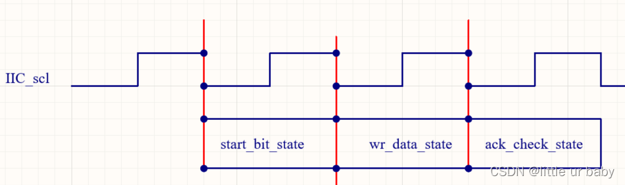
由于IIC_sda数据的变化点在IIC_scl的前一个周期(当前周期数据需要稳定可读取),而变化沿的产生又在同一个周期(设定),如果直接用IIC_scl来设计状态机的话,会出现如图情况(即需要在start_bit_state状态里同时设计上升沿和第一个要写的数据,非常不方便)。为了状态机的书写方便,用于设计状态机的驱动时钟相对IIC_scl移相90°(这样就可以在start_bit_state状态只设计上升沿,所有要写的数据都在wr_data_state状态里设计),具体看图(可以先看状态机再回头看这儿)
2.架构设计
IIC协议的目的是为了:
1.向某个IIC器件的某个存储单元写入数据;
2.从某个IIC器件的某个存储单元读出数据;
2.1 驱动逻辑模块
为了实现这两个功能,需要根据时序图,用两个线性序列机分别设计读和写的状态顺序和时序。其中,写控制信息、写存储单元地址、写数据均可以归结为写数据一个状态,具体状态划分如下:

写逻辑:空闲 --> 产生起始位 --> 写控制信息 --> 检查应答 --> 写存储器高位地址 --> 检查应答 --> 写存储器低位地址 --> 检查应答 --> 写数据 --> 检查应答 --> 产生结束位 --> 空闲
即: idel_state --> start_bit_state --> wr_data_state --> ack_check_state --> wr_data_state --> ack_check_state --> wr_data_state --> ack_check_state --> wr_data_state --> ack_check_state --> stop_bit_state --> idel_state_state
读逻辑:空闲 --> 产生起始位 --> 写控制信息 --> 检查应答 --> 写存储器高位地址 --> 检查应答 --> 写存储器低位地址 --> 检查应答 --> 产生起始位 --> 写控制信息 --> 检查应答 --> 读数据 --> 产生应答 -->产生结束位 --> 空闲
即: idel_state --> start_bit_state --> wr_data_state --> ack_check_state --> wr_data_state --> ack_check_state --> wr_data_state --> ack_check_state --> start_bit_state --> wr_data_state --> ack_check_state --> rd_data_state --> gen_noack_state--> stop_bit_state --> idel_state
从而,IIC的驱动模块架构如下:
其中,根据wr_sig / rd_sig 来产生开启一次读/写的完整操作,由cmd控制状态,通过时序逐个把IIC_id、wr_addr、rd_addr、wr_data通过write_data输出,通过接受trans_done信号来结束一次读/写操作。
2.2 底层逻辑模块
这一层模块用于接受驱动模块发出的命令(即状态指令),根据指令对接受的wr_data进行输出;设计8种状态需要对IIC_sda总线的输出和输入进行的操作。根据时序图,结合线性序列机和状态机进行编写即可,重点在于数据变化的时刻以及IIC_scl这种inout三态门的输入输出设计(前面已经介绍)。
3.代码设计
module IIC_design(
	input fpga_clk,//50MHz
	input rst_n ,
	input rate_sel ,
	input read_pulse ,
	input write_pulse ,
	input [7:0]write_data ,
	input [7:0]IIC_id ,
	input [15:0]wr_addr ,
	input [15:0]rd_addr ,

	output trans_done ,
	output [7:0]read_data ,
	output IIC_scl ,
	inout IIC_sda
);


//*******   IIC_scl设计      ******* //
wire clk_16M ;	//
wire clk_4M ;
wire clk_4M90 ;
wire clk_1M ;
wire clk_1M90 ;
wire clk_1600k ;
wire clk_400k ;//对应 scl 400kb/s 速率
wire clk_400k108 ;
wire clk_100k ;//对应 scl 100kb/s 速率
wire clk_100k108 ;
wire sda_clk ;//控制时序的时钟
wire drive_clk ; //产生cmd的时钟
//锁相环分频
 pll pll_inst1(
	.inclk0(fpga_clk),
	.c0(clk_16M),
	.c1(clk_4M),
	.c2(clk_1M)
	);
//10分频
fenpin_10 fenpin_10_inst1(
	.clk(clk_4M),
	.rst_n(rst_n),
	.outClk(clk_400k)
);
fenpin_10 fenpin_10_inst2(
	.clk(clk_1M),
	.rst_n(rst_n),
	.outClk(clk_100k)
);
fenpin_10 fenpin_10_inst3(
	.clk(clk_16M),
	.rst_n(rst_n),
	.outClk(clk_1600k)
);

fenpin_10_108du fenpin_10_108du_inst1(
	.clk(clk_4M),
	.rst_n(rst_n),
	.outClk(clk_400k108)
);
fenpin_10_108du fenpin_10_108du_inst2(
	.clk(clk_1M),
	.rst_n(rst_n),
	.outClk(clk_100k108)
);

//设置IIC总线时钟 400kb/s 或 100kb/s
assign IIC_scl = rate_sel ? clk_400k : clk_100k ;
assign sda_clk = rate_sel ? clk_1600k : clk_400k  ;
assign drive_clk = rate_sel ? clk_400k108 : clk_100k108 ;
//**********************************//

wire [7:0]rd_data ;
wire ack_result ;
wire [7:0]command ;
wire [7:0]wr_data ;
IIC_drive IIC_drive_inst(
	.fpga_clk(fpga_clk) ,//50MHz
	.drive_clk(drive_clk),
	.rst_n(rst_n) ,
	.wr_sig(write_pulse) ,
	.rd_sig(read_pulse) ,
	.wr_data(write_data) ,
	.rd_data(rd_data) ,
	.IIC_id(IIC_id) ,
	.wr_addr(wr_addr) ,
	.rd_addr(rd_addr) ,
	.trans_done(trans_done) ,
	.ack_result(ack_result) ,

	.cmd(command) ,
	.read_data(read_data) ,
	.write_data(wr_data)

);

IIC_underlying_logic IIC_underlying_logic_inst(

	.sda_clk(sda_clk) ,//
	.rst_n(rst_n) ,
	.cmd(command) ,
	.wr_data(wr_data) ,

	.rd_data(rd_data) ,
	.ack_result(ack_result) ,
	.trans_done(trans_done) ,
	.IIC_sda(IIC_sda)

);

endmodule
module IIC_drive(
input fpga_clk ,//50MHz
input drive_clk,
input rst_n ,
input wr_sig ,
input rd_sig ,
input [7:0]wr_data ,
input [7:0]rd_data ,
input [7:0]IIC_id ,
input [15:0]wr_addr ,
input [15:0]rd_addr ,
input trans_done ,
input ack_result ,
output reg [7:0]cmd ,
output reg [7:0]read_data ,
output reg [7:0]write_data
);
reg rd_pulse_reg ;
reg wr_pulse_reg ;
always@(posedge fpga_clk)
begin
wr_pulse_reg <= wr_sig ;
rd_pulse_reg <= rd_sig ;
end
reg read_sig ;
reg write_sig ;
always@(posedge fpga_clk or negedge rst_n)
if(!rst_n)
begin
read_sig <= 0 ;
end
else if( rd_pulse_reg == 0 && rd_sig == 1 )
read_sig <= 1 ;
else if( trans_done )
read_sig <= 0 ;
always@(posedge fpga_clk or negedge rst_n)
if(!rst_n)
begin
write_sig <= 0 ;
end
else if( wr_pulse_reg == 0 && wr_sig == 1 )
write_sig <= 1 ;
else if(trans_done)
write_sig <= 0 ;
//定义状态机7个状态参数
localparam idel_state = 8'b10000000 ; //空闲态:释放sda控制权
localparam start_bit_state = 8'b01000000 ; //产生起始位
localparam wr_data_state = 8'b00100000 ; // 写数据
localparam rd_data_state = 8'b00010000 ; // 读数据
localparam ack_check_state = 8'b00001000 ; //检查响应
localparam stop_bit_state = 8'b00000100 ; //产生停止位
localparam gen_ack_state = 8'b00000010 ; //产生停止位
localparam gen_noack_state = 8'b00000001 ; //产生停止位
//写逻辑
reg [5:0]write_cnt ;
//读逻辑
reg [5:0]read_cnt ;
always@(posedge drive_clk or negedge rst_n)
if(!rst_n)
begin
cmd <= idel_state ;
write_cnt <= 0 ;
write_data <= 0 ;
read_cnt <= 0 ;
read_data <= 0 ;
end
else if( write_sig == 1 )
begin
write_cnt <= write_cnt + 1 ;
if(ack_result)
begin
cmd <= ack_check_state ;
write_cnt <= 0 ;
end
else
begin
if(write_cnt == 1)
cmd <= idel_state ;//进入空闲态
else if ( write_cnt == 2 )
begin
cmd <= start_bit_state ;//产生起始位
end
else if ( write_cnt == 3 )
begin
cmd <= wr_data_state ;
write_data <= IIC_id ;//发送IIC器件ID
end
else if ( write_cnt == 11)
begin
cmd <= ack_check_state ;
end
else if ( write_cnt == 12 )
begin
cmd <= wr_data_state ;
write_data <= wr_addr[15:8] ;//写存储器高位地址
end
else if ( write_cnt == 20 )
begin
cmd <= ack_check_state ;
end
else if ( write_cnt == 21 )
begin
cmd <= wr_data_state ;
write_data <= wr_addr[7:0] ;//写存储器低位地址
end
else if ( write_cnt == 29 )
begin
cmd <= ack_check_state ;
end
else if ( write_cnt == 30 )
begin
cmd <= wr_data_state ;
write_data <= wr_data ; //写数据
end
else if ( write_cnt == 38 )
begin
cmd <= ack_check_state ;
end
else if ( write_cnt == 39 )
begin
cmd <= stop_bit_state ;//产生停止位
end
else if ( write_cnt == 40 )
begin
cmd <= idel_state ;//进入空闲态
write_cnt <= 0 ;
end
end
end
else if( read_sig == 1 )
begin
read_cnt <= read_cnt + 1 ;
if(ack_result)
begin
cmd <= ack_check_state ;
read_cnt <= 0 ;
end
else
begin
if(read_cnt == 1)
cmd <= idel_state ;//进入空闲态
else if ( read_cnt == 2 )
begin
cmd <= start_bit_state ;//产生起始位
end
else if ( read_cnt == 3 )
begin
cmd <= wr_data_state ;
write_data <= IIC_id ;//发送IIC器件ID 和写指令
end
else if ( read_cnt == 11)
begin
cmd <= ack_check_state ;
end
else if ( read_cnt == 12 )
begin
cmd <= wr_data_state ;
write_data <= rd_addr[15:8] ;//写存储器高位地址
end
else if ( read_cnt == 20 )
begin
cmd <= ack_check_state ;
end
else if ( read_cnt == 21 )
begin
cmd <= wr_data_state ;
write_data <= rd_addr[7:0] ;//写存储器低位地址
end
else if ( read_cnt == 29 )
begin
cmd <= ack_check_state ;
end
else if ( read_cnt == 30 )
begin
cmd <= start_bit_state ;
end
else if ( read_cnt == 31 )
begin
cmd <= wr_data_state ;
write_data <= ( IIC_id | 6'b000001 ) ;//写IIC器件ID 和读指令
end
else if ( read_cnt == 39 )
begin
cmd <= ack_check_state ;
end
else if ( read_cnt == 40 )
begin
cmd <= rd_data_state ;
end
else if ( read_cnt == 48 )
begin
cmd <= gen_noack_state ;
end
else if ( read_cnt == 49 )
begin
cmd <= stop_bit_state ;//产生停止位
read_data <= rd_data ; //寄存读数据
end
else if ( read_cnt == 50 )
begin
cmd <= idel_state ;//进入空闲态
write_cnt <= 0 ;
end
end
end
else
begin
cmd <= idel_state ;
write_cnt <= 0 ;
read_cnt <= 0 ;
end
endmodulemodule IIC_underlying_logic(
input sda_clk ,//
input rst_n ,
input [7:0]cmd ,
input [7:0]wr_data ,
output reg [7:0]rd_data ,
output reg ack_result ,
output reg trans_done ,
inout IIC_sda
);
//********* IIC_sda设计 ************//
reg sda_out ;
reg sda_ctrl;
assign IIC_sda = sda_ctrl ? ( sda_out ? 1'bz : 1'b0 ) : 1'bz ; //三态门,高阻态时,要么由总线上的上拉电阻拉至高电平,即输出/输出1;要么由从机拉至0,输入0;
//定义状态机7个状态参数
localparam idel_state = 8'b10000000 ; //空闲态:释放sda控制权
localparam start_bit_state = 8'b01000000 ; //产生起始位
localparam wr_data_state = 8'b00100000 ; // 写数据
localparam rd_data_state = 8'b00010000 ; // 读数据
localparam ack_check_state = 8'b00001000 ; //检查响应
localparam stop_bit_state = 8'b00000100 ; //产生停止位
localparam gen_ack_state = 8'b00000010 ; //产生停止位
localparam gen_noack_state = 8'b00000001 ; //产生停止位
reg [7:0]rw_state ;//实时状态
always@( posedge sda_clk or negedge rst_n )
if(!rst_n)
begin
rw_state <= idel_state ;
end
else
begin
if( cmd & idel_state )
rw_state <= idel_state ;
else if ( cmd & start_bit_state )
rw_state <= start_bit_state ;
else if ( cmd & wr_data_state )
rw_state <= wr_data_state ;
else if ( cmd & rd_data_state )
rw_state <= rd_data_state ;
else if ( cmd & ack_check_state )
rw_state <= ack_check_state ;
else if ( cmd & stop_bit_state )
rw_state <= stop_bit_state ;
else if ( cmd & gen_ack_state )
rw_state <= gen_ack_state ;
else if ( cmd & gen_noack_state )
rw_state <= gen_noack_state ;
end
reg [5:0]cnt ;
always@( posedge sda_clk or negedge rst_n )
if(!rst_n)
begin
sda_out <= 1'b1 ;
sda_ctrl<= 1'b0 ;
trans_done <= 0 ;
ack_result <= 0 ;
rd_data <= 0 ;
cnt <= 1'b0 ;
end
else
begin
case(rw_state)
idel_state:
begin
cnt <= 1'b0 ;
sda_ctrl<= 1'b0 ;//释放sda控制权
sda_out <= 1'b1 ;
trans_done <= 0 ;
ack_result <= 0 ;
end
start_bit_state:
begin
sda_ctrl<= 1'b1 ;//获取sda控制权
if(cnt == 2 )
begin
sda_out <= 1'b0 ;
end
cnt <= cnt + 1 ;
if(cnt == 3 )
cnt <= 0 ;
end
wr_data_state:
begin
sda_ctrl<= 1'b1 ;//获取sda控制权
if( cnt == 0 )
sda_out <= wr_data[7] ;
else if ( cnt == 4 )
sda_out <= wr_data[6] ;
else if ( cnt == 8 )
sda_out <= wr_data[5] ;
else if ( cnt == 12 )
sda_out <= wr_data[4] ;
else if ( cnt == 16 )
sda_out <= wr_data[3] ;
else if ( cnt == 20 )
sda_out <= wr_data[2] ;
else if ( cnt == 24 )
sda_out <= wr_data[1] ;
else if ( cnt == 28 )
sda_out <= wr_data[0] ;
cnt <= cnt +1 ;
if( cnt == 31 )
cnt <= 0 ;
end
rd_data_state:
begin
sda_ctrl<= 1'b0 ;//释放sda控制权
if( cnt == 2 )
rd_data[7] <= IIC_sda ;
else if ( cnt == 6 )
rd_data[6] <= IIC_sda ;
else if ( cnt == 10 )
rd_data[5] <= IIC_sda ;
else if ( cnt == 14 )
rd_data[4] <= IIC_sda ;
else if ( cnt == 18 )
rd_data[3] <= IIC_sda ;
else if ( cnt == 22 )
rd_data[2] <= IIC_sda ;
else if ( cnt == 26 )
rd_data[1] <= IIC_sda ;
else if ( cnt == 30 )
rd_data[0] <= IIC_sda ;
cnt <= cnt +1 ;
if( cnt == 31 )
cnt <= 0 ;
end
ack_check_state:
begin
sda_ctrl<= 1'b0 ;//释放sda控制权
if( cnt == 2 )
ack_result <= IIC_sda ;
cnt <= cnt + 1 ;
if( cnt == 3 )
cnt <= 0 ;
end
stop_bit_state:
begin
sda_ctrl<= 1'b1 ;//获取sda控制权
sda_out <= 1'b0 ;
if( cnt == 2 )
begin
sda_ctrl<= 1'b0 ;//释放sda控制权
end
cnt <= cnt + 1 ;
if(cnt == 3 )
begin
cnt <= 0 ;
trans_done <= 1 ;
end
end
gen_ack_state:
begin
sda_ctrl<= 1'b1 ;//获取sda控制权
sda_out <= 1'b0 ;
cnt <= cnt + 1 ;
if(cnt == 3 )
cnt <= 0 ;
end
gen_noack_state:
begin
sda_ctrl<= 1'b1 ;//获取sda控制权
sda_out <= 1'b1 ;
cnt <= cnt + 1 ;
if(cnt == 3 )
cnt <= 0 ;
end
default: ;
endcase
end
endmodule`timescale 1ns/1ns
module IIC_design_tb();
reg fpga_clk ;
reg rst_n ;
reg rate_sel ;
reg read_pulse ;
reg write_pulse ;
reg [7:0]write_data ;
reg [7:0]IIC_id ;
reg [15:0]wr_addr ;
reg [15:0]rd_addr ;
wire trans_done ;
wire [7:0]read_data ;
wire IIC_scl ;
wire IIC_sda ;
pullup(IIC_sda) ;
IIC_design IIC_design_inst(
.fpga_clk(fpga_clk),//50MHz
.rst_n(rst_n) ,
.rate_sel(rate_sel) ,
.read_pulse(read_pulse) ,
.write_pulse(write_pulse) ,
.write_data(write_data) ,
.IIC_id(IIC_id) ,
.wr_addr(wr_addr) ,
.rd_addr(rd_addr) ,
.trans_done(trans_done) ,
.read_data(read_data) ,
.IIC_scl(IIC_scl) ,
.IIC_sda(IIC_sda)
);
M24LC04B M24LC04B_inst(
.A0(0),
.A1(0),
.A2(0),
.WP(0),
.SDA(IIC_sda),
.SCL(IIC_scl),
.RESET(~rst_n)
);
initial fpga_clk = 1 ;
always #10 fpga_clk = ! fpga_clk ;
initial begin
rst_n = 0 ;
rate_sel = 1 ;
read_pulse = 0 ;
write_pulse = 0 ;
write_data = 0 ;
IIC_id = 0 ;
wr_addr = 0 ;
rd_addr = 0 ;
#200 ;
rst_n = 1 ;
#1000 ;
IIC_id = 8'b10100110 ;
wr_addr = 16'd1 ;
write_data = 8'd20 ;
write_pulse = 1 ;
#100 ;
write_pulse = 0 ;
#125000 ;
rd_addr = 16'd1 ;
read_pulse = 1 ;
#100 ;
read_pulse = 0 ;
#250000 ;
end
endmodule4.板级验证
为验证代码可行性,设计如下验证程序 : fpga通过IIC协议向内部EEPROM存储器的某个单元写入数据,并能读取出来。
设置两个按键:key1 产生写信号write_sig ;key2 产生写信号read_sig ;
通过 in-systerm probes and sources 功能验证:
引脚分配要注意IIC_scl和IIC_sda的引脚要根据手册对应连接,且IIC_id也要对应(这里eeprom存储器M24LC04B对应的器件ID为A0)
module IIC_eeprom(
input clk ,
input rst_n ,
input [1:0]key ,
output IIC_scl ,
inout IIC_sda
);
wire [7:0]read_data ;
wire [15:0]addr ;
wire [7:0]write_data ;
wire write_sig ;
wire read_sig ;
//assign addr = 16'd1 ;
//assign write_data = 8'd250 ;
IIC_design IIC_design_inst(
.fpga_clk(clk),//50MHz
.rst_n(rst_n) ,
.rate_sel(1) ,
.read_pulse(~read_sig) ,
.write_pulse(~write_sig) ,
.write_data(write_data) ,
.IIC_id(8'ha0) ,
.wr_addr(addr) ,
.rd_addr(addr) ,
.trans_done() ,
.read_data(read_data) ,
.IIC_scl(IIC_scl) ,
.IIC_sda(IIC_sda)
);
buttopn_debounde buttopn_debounde_inst1(
.clk(clk),
.tx(key[1]),
.reset(rst_n),
.bd_tx(write_sig)
);
buttopn_debounde buttopn_debounde_inst2(
.clk(clk),
.tx(key[0]),
.reset(rst_n),
.bd_tx(read_sig)
);
insys_wrdata insys_wrdata_inst(
.probe(), // probes.probe
.source(write_data) // 向addr写入数据
);
insys_rddata insys_rddata_inst(
.probe(read_data), // probes.probe
.source(addr) // 手动输入地址,读取addr的数据
);
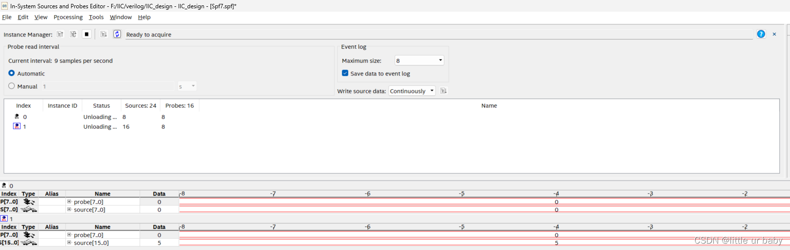
endmodule初始状态:
修改addr:
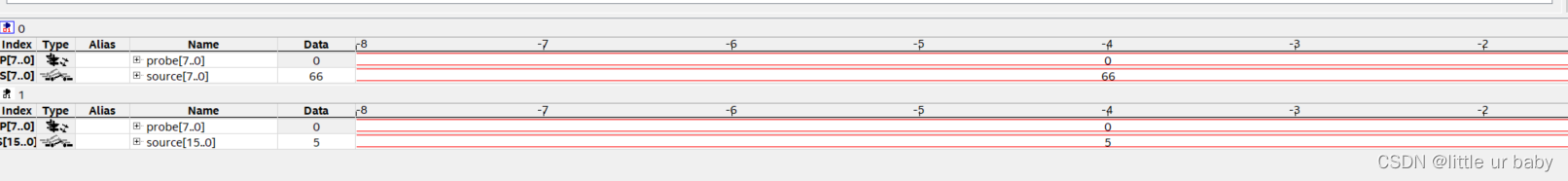
向addr写入数据66:
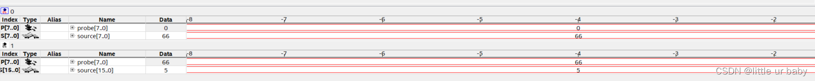
从addr读出数据:
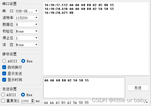
串口-fpga-eeprom芯片
功能:
上位机(PC)通过uart串口协议与FPGA通信,发送想要向eeprom芯片写入的地址和数据,以及想要读取某地址的数据。FPGA通过IIC协议与eeprom芯片M24LC04B通信,读写数据。
EEPROM的全称是“电可擦除可编程只读存储器”,即Electrically Erasable Programmable Read-Only Memory。是相对于紫外擦除的rom来讲的。但是今天已经存在多种EEPROM的变种,变成了一类存储器的统称。这种rom的特点是可以随机访问和修改任何一个字节,可以往每个bit中写入0或者1。这是最传统的一种EEPROM,掉电后数据不丢失,可以保存100年,可以擦写100w次。具有较高的可靠性,但是电路复杂/成本也高。因此目前的EEPROM都是几十千字节到几百千字节的,绝少有超过512K的。
flash属于广义的EEPROM,因为它也是电擦除的rom。但是为了区别于一般的按字节为单位的擦写的EEPROM,我们都叫它flash。flash做的改进就是擦除时不再以字节为单位,而是以块为单位,一次简化了电路,数据密度更高,降低了成本。上M的rom一般都是flash。
要求:
① 要有一定的抗干扰能力
②能舍弃传输错误的数据,又不丢失正确的数据
方法:
① 定义一个传输帧(协议),有帧头帧尾(最好定义为5 或 A 这两个电平不断翻转的),这个帧包括地址、器件ID、读写数据等。
② 利用移位寄存器,每接受一个新的数据,就对移位寄存器内所有数据进行一次帧判别,这样就不会丢失。
实现:
定义帧格式如下:
帧头 IIC_id haddr laddr option data 帧尾
帧头定义为:AA AA 帧尾定义为:55
option定义: 读(5A);写(A5)
整帧:
AA AA ID haddr laddr r/w data 55
设计:
每次uart接受模块接受到一个新数据,就通过移位寄存器保存下来,并进行整帧检测,如果符合帧格式,就产生读/写脉冲,通过IIC模块对eeprom存储器进行读写操作,然后通过uart发送模块传输到上位机。
代码:
module uart_IIC_eeprom(
	input fpga_clk ,
	input rst_n ,

	input uart_rx ,
	output rx_done ,
	output uart_tx ,

	output IIC_scl ,
	inout IIC_sda

);


//receive uart data
//wire rx_done ;
wire [7:0]rx_data ;
uart_receive uart_rec_inst(
    .clk(fpga_clk) ,
    .reset(rst_n) ,
    .baud_rate('d5) ,//115200
    .uart_rx(uart_rx),
    .data(rx_data) ,
    .rx_done(rx_done)
    );

//Shift register
reg [7:0]rec_shift_reg[7:0] ;
reg rw_flag ;
wire iic_done ;
always@(posedge fpga_clk or negedge rst_n)
if(!rst_n)
	begin
		rec_shift_reg[0] <= 0 ;
		rec_shift_reg[1] <= 0 ;
		rec_shift_reg[2] <= 0 ;
		rec_shift_reg[3] <= 0 ;
		rec_shift_reg[4] <= 0 ;
		rec_shift_reg[5] <= 0 ;
		rec_shift_reg[6] <= 0 ;
		rec_shift_reg[7] <= 0 ;
		rw_flag <= 0 ;
	end
else if(rx_done)
	begin
		rec_shift_reg[0] <= rec_shift_reg[1] ;
 		rec_shift_reg[1] <= rec_shift_reg[2] ;
		rec_shift_reg[2] <= rec_shift_reg[3] ;
		rec_shift_reg[3] <= rec_shift_reg[4] ;
		rec_shift_reg[4] <= rec_shift_reg[5] ;
		rec_shift_reg[5] <= rec_shift_reg[6] ;
		rec_shift_reg[6] <= rec_shift_reg[7] ;
		rec_shift_reg[7] <= rx_data ;
		rw_flag <= 1 ;
	end
else if(iic_done)
		rw_flag <= 0 ;

reg [7:0]IIC_id ;
reg [15:0]write_addr ;
reg [15:0]read_addr ;
reg [7:0]write_data ;
reg [7:0]read_data ;
wire [7:0]rd_data ;
reg write_pulse ;
reg read_pulse ;

IIC_design IIC_rw(
	.fpga_clk(fpga_clk),//50MHz
	.rst_n(rst_n) ,
	.rate_sel(1) ,
	.read_pulse(read_pulse) ,
	.write_pulse(write_pulse) ,
	.write_data(write_data) ,
	.IIC_id(IIC_id) ,
	.wr_addr(write_addr) ,
	.rd_addr(read_addr) ,

	.trans_done(iic_done) ,
	.read_data(rd_data) ,
	.IIC_scl(IIC_scl) ,
	.IIC_sda(IIC_sda)
);

wire uart_send_done ;
reg uart_send_en ;
uart_send uart_send(
    .clk(fpga_clk),
    .reset(rst_n),
    .data(read_data),
    .send_en(uart_send_en),
    .baud_rate(5),//115200
    .uart_tx(uart_tx),
    .tx_done(uart_send_done)
);

//Parsing frames
localparam frames_header = 8'hAA ;
localparam frames_tail   = 8'h55 ;
localparam read_option   = 8'h5A ;
localparam write_option  = 8'hA5 ;
reg [15:0]wr_cnt ;
reg [15:0]rd_cnt ;
always@(posedge fpga_clk or negedge rst_n)
if(!rst_n)
	begin
		IIC_id <= 0 ;
		write_addr <= 0 ;
		read_addr <= 0 ;
		write_data <= 0;
		read_data <= 0 ;
		write_pulse <= 0 ;
		read_pulse <= 0 ;
		//uart_send_en <= 0 ;
		wr_cnt <= 0 ;
		rd_cnt <= 0 ;
	end

else if( rw_flag )
	begin
		if ( (rec_shift_reg[0] == frames_header) && (rec_shift_reg[1] == frames_header) && (rec_shift_reg[7] == frames_tail) )
			begin
				IIC_id <= rec_shift_reg[2] ;
				if(rec_shift_reg[5] == write_option )
					begin
						write_addr <= { rec_shift_reg[3] , rec_shift_reg[4] } ;
						write_data <= rec_shift_reg[6] ;
						wr_cnt <= wr_cnt + 1 ;
						//write signal
						if( wr_cnt < 3 )
							write_pulse <= 1 ;
						else if(iic_done)
							begin
								wr_cnt <= 0 ;

							end
						else
							write_pulse <= 0 ;
					end
				else if ( rec_shift_reg[5] == read_option )
					begin
						read_addr <= { rec_shift_reg[3] , rec_shift_reg[4] } ;
						//read signal
						rd_cnt <= rd_cnt + 1 ;
						if(iic_done)
							begin
								read_data <= rd_data ;
								read_pulse <= 0 ;
								//uart_send_en <= 1 ;
								rd_cnt <= 0 ;

							end
						//else if(uart_send_done)
						//	uart_send_en <= 0 ;
						else if(rd_cnt <3)
							read_pulse <= 1 ;
						else
							read_pulse <= 0 ;
					end
			end
	end
else
	begin
		write_pulse <= 0 ;
		read_pulse <= 0 ;
		//uart_send_en <= 0 ;
		wr_cnt <= 0 ;
		rd_cnt <= 0 ;
	end

always@(posedge fpga_clk or negedge rst_n)
if(!rst_n)
	uart_send_en <= 0 ;
else if(iic_done && (rec_shift_reg[5] == read_option) )
	uart_send_en <= 1 ;
else if(uart_send_done)
	uart_send_en <= 0 ;

endmodule
板级验证成功。
可是可是,这样用分频器设计出来的sda_clk和drive_clk 时钟质量都很差,因为该时钟是从寄存器发出的信号,不是利用fpga的全局时钟资源,所以到达其他不同的寄存器的延时会因为布线长度的不同而不一样。这里上板验证可以成功,因为本设计对时钟质量要求不高。
重新设计时,应该用fpga_clk或者PLL出来的时钟来设计。
优化设计
思路
为了提高时钟质量,这里改变设计思路,选择用PLL出来的10MHz时钟作为驱动时钟,如图,只要把状态的转移设置从时钟下降沿开始,就可以兼顾起始位状态需要在scl高电平改变数据,读写数据需要在scl低电平修改数据的问题了。
module IIC_design(
	input fpga_clk ,
	input rst_n ,
	input read_pulse ,
	input write_pulse ,
	input [7:0]write_data ,
	input [7:0]IIC_id ,
	input [15:0]wr_addr ,
	input [15:0]rd_addr ,

	output trans_done ,
	output [7:0]read_data ,
	output IIC_scl ,
	inout IIC_sda
);

wire [7:0]wr_data ;
wire [7:0]rd_data ;
wire [7:0]command ;
IIC_drive IIC_drive_inst(
	.fpga_clk(fpga_clk) ,
	.rst_n(rst_n) ,

	.write_sig(write_pulse) ,
	.read_sig(read_pulse) ,
	.IIC_id(IIC_id) ,
	.wr_addr(wr_addr) ,
	.rd_addr(rd_addr) ,
	.wr_data(write_data) ,
	.rd_data(rd_data) ,
	.trans_done(trans_done) ,

	.read_data(read_data) ,
	.write_data(wr_data) ,
	.cmd(command)

);

IIC_underlying_logic IIC_underlying_logic_inst(
	.fpga_clk(fpga_clk) ,
	.rst_n(rst_n) ,

	.write_data(wr_data) ,
	.cmd(command),

	.read_data(rd_data) ,
	.trans_done(trans_done) ,
	.ack_result() ,

	.IIC_scl(IIC_scl) ,
	.IIC_sda(IIC_sda)
);

endmodule
module IIC_drive(
input fpga_clk ,
input rst_n ,
input write_sig ,
input read_sig ,
input [7:0]IIC_id ,
input [15:0]wr_addr ,
input [15:0]rd_addr ,
input [7:0]wr_data ,
input [7:0]rd_data ,
input trans_done ,
output reg[7:0]read_data ,
output reg[7:0]write_data ,
output reg [7:0]cmd
);
wire clk_10m ;
//PLL
pll pll_inst(
.inclk0(fpga_clk),
.c0(clk_10m)
);
// IIC rate : 400k clk : 10Mhz
localparam cnt400k_max = 10000000 / 400000 ;
reg [15:0]IIC_cnt ;
always@(posedge clk_10m or negedge rst_n)
if(!rst_n)
IIC_cnt <= 0 ;
else if( IIC_cnt >= 24 )
IIC_cnt <= 0 ;
else
IIC_cnt <= IIC_cnt + 1 ;
//定义状态机8个状态参数
localparam idel_state = 8'b10000000 ; //空闲态:释放sda控制权
localparam start_bit_state = 8'b01000000 ; //产生起始位
localparam wr_data_state = 8'b00100000 ; // 写数据
localparam rd_data_state = 8'b00010000 ; // 读数据
localparam ack_check_state = 8'b00001000 ; //检查响应
localparam stop_bit_state = 8'b00000100 ; //产生停止位
localparam gen_ack_state = 8'b00000010 ; //产生响应位
localparam gen_noack_state = 8'b00000001 ; //产生非响应位
//移位寄存器。寄存读写信号
reg rd_pulse_reg ;
reg wr_pulse_reg ;
always@(posedge fpga_clk)
begin
wr_pulse_reg <= write_sig ;
rd_pulse_reg <= read_sig ;
end
reg rd_sig ;
reg wr_sig ;
always@(posedge fpga_clk or negedge rst_n)
if(!rst_n)
rd_sig <= 0 ;
else if( rd_pulse_reg == 0 && read_sig == 1 )
rd_sig <= 1 ;
else if( trans_done )
rd_sig <= 0 ;
always@(posedge fpga_clk or negedge rst_n)
if(!rst_n)
wr_sig <= 0 ;
else if( wr_pulse_reg == 0 && write_sig == 1 )
wr_sig <= 1 ;
else if( trans_done )
wr_sig <= 0 ;
//读写逻辑
reg [5:0]write_cnt ;
reg [5:0]read_cnt ;
always@(posedge clk_10m or negedge rst_n)
if(!rst_n)
begin
cmd <= idel_state ;
write_data <= 0 ;
read_data <= 0 ;
write_cnt <= 0 ;
read_cnt <= 0 ;
end
else if( wr_sig )
begin
if(write_cnt == 0)
cmd <= idel_state ; //空闲态
else if ( write_cnt == 1 )
begin
cmd <= start_bit_state ;//产生起始位
end
else if ( write_cnt == 2 )
begin
cmd <= wr_data_state ;
write_data <= IIC_id ;//发送IIC器件ID
end
else if ( write_cnt == 10)
begin
cmd <= ack_check_state ;
end
else if ( write_cnt == 11 )
begin
cmd <= wr_data_state ;
write_data <= wr_addr[15:8] ;//写存储器高位地址
end
else if ( write_cnt == 19 )
begin
cmd <= ack_check_state ;
end
else if ( write_cnt == 20 )
begin
cmd <= wr_data_state ;
write_data <= wr_addr[7:0] ;//写存储器低位地址
end
else if ( write_cnt == 28 )
begin
cmd <= ack_check_state ;
end
else if ( write_cnt == 29 )
begin
cmd <= wr_data_state ;
write_data <= wr_data ; //写数据
end
else if ( write_cnt == 37 )
begin
cmd <= ack_check_state ;
end
else if ( write_cnt == 38 )
begin
cmd <= stop_bit_state ;//产生停止位
end
if(IIC_cnt == 23)
write_cnt <= write_cnt + 1 ;
if(write_cnt >= 39)
begin
write_cnt <= 0 ;
cmd <= idel_state ; //空闲态
end
end
else if( rd_sig )
begin
if(read_cnt == 0)
cmd <= idel_state ; //空闲态
else if ( read_cnt == 1 )
begin
cmd <= start_bit_state ;//产生起始位
end
else if ( read_cnt == 2 )
begin
cmd <= wr_data_state ;
write_data <= IIC_id ;//发送IIC器件ID
end
else if ( read_cnt == 10)
begin
cmd <= ack_check_state ;
end
else if ( read_cnt == 11 )
begin
cmd <= wr_data_state ;
write_data <= rd_addr[15:8] ;//写存储器高位地址
end
else if ( read_cnt == 19 )
begin
cmd <= ack_check_state ;
end
else if ( read_cnt == 20 )
begin
cmd <= wr_data_state ;
write_data <= rd_addr[7:0] ;//写存储器低位地址
end
else if ( read_cnt == 28 )
begin
cmd <= ack_check_state ;
end
else if( read_cnt == 29 )
cmd <= start_bit_state ;
else if ( read_cnt == 30 )
begin
cmd <= wr_data_state ;
write_data <= (IIC_id | 8'b00000001 ) ; //写IIC器件ID 和读指令
end
else if ( read_cnt == 38 )
begin
cmd <= ack_check_state ;
end
else if ( read_cnt == 39 )
begin
cmd <= rd_data_state ;//
end
else if ( read_cnt == 47 )
begin
cmd <= gen_noack_state ;//
end
else if ( read_cnt == 48 )
begin
cmd <= stop_bit_state ;
read_data <= rd_data ;
end
if(IIC_cnt == 23)
read_cnt <= read_cnt + 1 ;
if ( read_cnt == 49 )
begin
cmd <= idel_state ;
read_cnt <= 0 ;
end
end
else
begin
cmd <= idel_state ;
write_cnt <= 0 ;
read_cnt <= 0 ;
end
endmodulemodule IIC_underlying_logic(
input fpga_clk ,
input rst_n ,
input [7:0]write_data ,
input [7:0]cmd ,
output reg [7:0]read_data ,
output reg trans_done ,
output reg ack_result ,
output reg IIC_scl ,
inout IIC_sda
);
wire clk_10m ;
//PLL
pll pll_inst(
.inclk0(fpga_clk),
.c0(clk_10m)
);
// IIC rate : 100k 400k clk : 10Mhz
localparam cnt400k_max = 10000000 / 400000 ;
localparam cnt100k_max = 10000000 / 100000 ;
reg [15:0]IIC_cnt ;
always@(posedge clk_10m or negedge rst_n)
if(!rst_n)
IIC_cnt <= 0 ;
else if( IIC_cnt >= 24 )
IIC_cnt <= 0 ;
else
IIC_cnt <= IIC_cnt + 1 ;
//IIC SCLK
always@(posedge clk_10m or negedge rst_n)
if(!rst_n)
IIC_scl <= 0 ;
else if( IIC_cnt == 24 | IIC_cnt == 11 )
IIC_scl <= !IIC_scl ;
//IIC SDATA
reg sda_ctrl ;
reg sda_out ;
assign IIC_sda = sda_ctrl ? ( sda_out ? 1'bz : 1'b0 ) : 1'bz ; //三态门,高阻态时,要么由总线上的上拉电阻拉至高电平,即输出/输出1;要么由从机拉至0,输入0;
//定义状态机8个状态参数
localparam idel_state = 8'b10000000 ; //空闲态:释放sda控制权
localparam start_bit_state = 8'b01000000 ; //产生起始位
localparam wr_data_state = 8'b00100000 ; // 写数据
localparam rd_data_state = 8'b00010000 ; // 读数据
localparam ack_check_state = 8'b00001000 ; //检查响应
localparam stop_bit_state = 8'b00000100 ; //产生停止位
localparam gen_ack_state = 8'b00000010 ; //产生响应位
localparam gen_noack_state = 8'b00000001 ; //产生非响应位
//状态机实时状态
wire [7:0]rw_state;
assign rw_state = cmd ;
reg [8:0]state_cnt ;
always@(posedge clk_10m or negedge rst_n)
if(!rst_n)
begin
sda_ctrl <= 0 ;
sda_out <= 1 ;
trans_done <= 0 ;
ack_result <= 0 ;
read_data <= 0 ;
state_cnt <= 0 ;
end
else
begin
case(rw_state)
idel_state :
begin
sda_ctrl <= 0 ;
trans_done <= 0 ;
ack_result <= 0 ;
state_cnt <= 0 ;
end
start_bit_state :
begin
sda_ctrl <= 1 ;
state_cnt <= state_cnt + 1 ;
if( state_cnt >= 17 )
sda_out <= 0 ;
else
sda_out <= 1 ;
if ( state_cnt >= 24 )
state_cnt <= 0 ;
end
wr_data_state :
begin
sda_ctrl <= 1 ;
state_cnt <= state_cnt + 1 ;
if( state_cnt == 5 )
sda_out <= write_data[7] ;
else if( state_cnt == 30 )
sda_out <= write_data[6] ;
else if( state_cnt == 55 )
sda_out <= write_data[5] ;
else if( state_cnt == 80 )
sda_out <= write_data[4] ;
else if( state_cnt == 105 )
sda_out <= write_data[3] ;
else if( state_cnt == 130 )
sda_out <= write_data[2] ;
else if( state_cnt == 155 )
sda_out <= write_data[1] ;
else if( state_cnt == 180 )
sda_out <= write_data[0] ;
if( state_cnt >= 199 )
state_cnt <= 0 ;
end
rd_data_state :
begin
sda_ctrl <= 0 ;
state_cnt <= state_cnt + 1 ;
if( state_cnt == 15 )
read_data[7] <= IIC_sda ;
else if( state_cnt == 40 )
read_data[6] <= IIC_sda ;
else if( state_cnt == 65 )
read_data[5] <= IIC_sda ;
else if( state_cnt == 90 )
read_data[4] <= IIC_sda ;
else if( state_cnt == 115 )
read_data[3] <= IIC_sda ;
else if( state_cnt == 140 )
read_data[2] <= IIC_sda ;
else if( state_cnt == 165 )
read_data[1] <= IIC_sda ;
else if( state_cnt == 190 )
read_data[0] <= IIC_sda ;
if( state_cnt >= 199 )
state_cnt <= 0 ;
end
ack_check_state :
begin
sda_ctrl <= 0 ;//释放sda控制权
state_cnt <= state_cnt + 1 ;
if( state_cnt == 1 )
ack_result <= IIC_sda ;
if(state_cnt >= 24)
state_cnt <= 0 ;
end
stop_bit_state :
begin
sda_ctrl<= 1'b1 ;//获取sda控制权
sda_out <= 1'b0 ;
state_cnt <= state_cnt + 1 ;
if( state_cnt >= 17 )
sda_out <= 1 ;
else
sda_out <= 0 ;
if ( state_cnt >=24 )
begin
state_cnt <= 0 ;
trans_done <= 1 ;
end
end
gen_ack_state :
begin
sda_ctrl<= 1'b1 ;//获取sda控制权
state_cnt <= state_cnt + 1 ;
if( state_cnt >= 10 )
sda_out <= 1'b0 ;
if(state_cnt >= 24 )
state_cnt <= 0 ;
end
gen_noack_state :
begin
sda_ctrl<= 1'b1 ;//获取sda控制权
state_cnt <= state_cnt + 1 ;
if( state_cnt >= 10 )
sda_out <= 1'b1 ;
if(state_cnt >= 24 )
state_cnt <= 0 ;
end
default: ;
endcase
end
endmodule//***************** ******************//
// 串口波特率:115200 //
// 通信帧格式: //
// AA AA ID HA LA RW DA 55 //
// 其中,AA AA 为帧头;55为帧尾; //
// ID为IIC器件ID,HA、LA为存储器地址 //
// RW为读写控制,读:5A ;写:A5 //
// DA为要写入的数据,读的时候可为任意值 //
// ********************************* //
module uart_IIC_eeprom(
input fpga_clk ,
input rst_n ,
input uart_rx ,
output rx_done ,
output uart_tx ,
output IIC_scl ,
inout IIC_sda
);
//receive uart data
//wire rx_done ;
wire [7:0]rx_data ;
uart_receive uart_rec_inst(
.clk(fpga_clk) ,
.reset(rst_n) ,
.baud_rate('d5) ,//115200
.uart_rx(uart_rx),
.data(rx_data) ,
.rx_done(rx_done)
);
//Shift register
reg [7:0]rec_shift_reg[7:0] ;
reg rw_flag ;
wire iic_done ;
always@(posedge fpga_clk or negedge rst_n)
if(!rst_n)
begin
rec_shift_reg[0] <= 0 ;
rec_shift_reg[1] <= 0 ;
rec_shift_reg[2] <= 0 ;
rec_shift_reg[3] <= 0 ;
rec_shift_reg[4] <= 0 ;
rec_shift_reg[5] <= 0 ;
rec_shift_reg[6] <= 0 ;
rec_shift_reg[7] <= 0 ;
rw_flag <= 0 ;
end
else if(rx_done)
begin
rec_shift_reg[0] <= rec_shift_reg[1] ;
rec_shift_reg[1] <= rec_shift_reg[2] ;
rec_shift_reg[2] <= rec_shift_reg[3] ;
rec_shift_reg[3] <= rec_shift_reg[4] ;
rec_shift_reg[4] <= rec_shift_reg[5] ;
rec_shift_reg[5] <= rec_shift_reg[6] ;
rec_shift_reg[6] <= rec_shift_reg[7] ;
rec_shift_reg[7] <= rx_data ;
rw_flag <= 1 ;
end
else if(iic_done)
rw_flag <= 0 ;
reg [7:0]IIC_id ;
reg [15:0]write_addr ;
reg [15:0]read_addr ;
reg [7:0]write_data ;
reg [7:0]read_data ;
wire [7:0]rd_data ;
reg write_pulse ;
reg read_pulse ;
IIC_design IIC_rw(
.fpga_clk(fpga_clk),//50MHz
.rst_n(rst_n) ,
.read_pulse(read_pulse) ,
.write_pulse(write_pulse) ,
.write_data(write_data) ,
.IIC_id(IIC_id) ,
.wr_addr(write_addr) ,
.rd_addr(read_addr) ,
.trans_done(iic_done) ,
.read_data(rd_data) ,
.IIC_scl(IIC_scl) ,
.IIC_sda(IIC_sda)
);
wire uart_send_done ;
reg uart_send_en ;
uart_send uart_send(
.clk(fpga_clk),
.reset(rst_n),
.data(read_data),
.send_en(uart_send_en),
.baud_rate(5),//115200
.uart_tx(uart_tx),
.tx_done(uart_send_done)
);
//Parsing frames
localparam frames_header = 8'hAA ;
localparam frames_tail = 8'h55 ;
localparam read_option = 8'h5A ;
localparam write_option = 8'hA5 ;
reg [15:0]wr_cnt ;
reg [15:0]rd_cnt ;
always@(posedge fpga_clk or negedge rst_n)
if(!rst_n)
begin
IIC_id <= 0 ;
write_addr <= 0 ;
read_addr <= 0 ;
write_data <= 0;
read_data <= 0 ;
write_pulse <= 0 ;
read_pulse <= 0 ;
wr_cnt <= 0 ;
rd_cnt <= 0 ;
end
else if( rw_flag )
begin
if ( (rec_shift_reg[0] == frames_header) && (rec_shift_reg[1] == frames_header) && (rec_shift_reg[7] == frames_tail) )
begin
IIC_id <= rec_shift_reg[2] ;
if(rec_shift_reg[5] == write_option )
begin
write_addr <= { rec_shift_reg[3] , rec_shift_reg[4] } ;
write_data <= rec_shift_reg[6] ;
wr_cnt <= wr_cnt + 1 ;
//write signal
if( wr_cnt < 3 )
write_pulse <= 1 ;
else if(iic_done)
begin
wr_cnt <= 0 ;
end
else
write_pulse <= 0 ;
end
else if ( rec_shift_reg[5] == read_option )
begin
read_addr <= { rec_shift_reg[3] , rec_shift_reg[4] } ;
//read signal
rd_cnt <= rd_cnt + 1 ;
if(iic_done)
begin
read_data <= rd_data ;
read_pulse <= 0 ;
rd_cnt <= 0 ;
end
else if(rd_cnt <3)
read_pulse <= 1 ;
else
read_pulse <= 0 ;
end
end
end
else
begin
write_pulse <= 0 ;
read_pulse <= 0 ;
wr_cnt <= 0 ;
rd_cnt <= 0 ;
end
always@(posedge fpga_clk or negedge rst_n)
if(!rst_n)
uart_send_en <= 0 ;
else if(iic_done && (rec_shift_reg[5] == read_option) )
uart_send_en <= 1 ;
else if(uart_send_done)
uart_send_en <= 0 ;
endmodulemodule uart_receive(
clk ,
reset ,
baud_rate ,
uart_rx,
data ,
rx_done
);
input clk ;
input reset ;
input [2:0]baud_rate ;
input uart_rx ;
output reg [7:0]data ;
output reg rx_done ;
reg [2:0]r_data[7:0] ;
reg [2:0]sta_bit ;
reg [2:0]sto_bit ;
reg [17:0]bit_tim ;
always@(baud_rate)
begin
case(baud_rate)
3'd0 : bit_tim = 1000000000/300/20 ;
3'd1 : bit_tim = 1000000000/1200/20 ;
3'd2 : bit_tim = 1000000000/2400/20 ;
3'd3 : bit_tim = 1000000000/9600/20 ;
3'd4 : bit_tim = 1000000000/19200/20 ;
3'd5 : bit_tim = 1000000000/115200/20 ;
default bit_tim = 1000000000/9600/20 ;
endcase
end
wire [17:0]bit_tim_16 ;
assign bit_tim_16 = bit_tim / 16;
wire [8:0]bit16_mid ;
assign bit16_mid = bit_tim_16 / 2 ;
reg [1:0]edge_detect ;
always @( posedge clk or negedge reset )
begin
if (!reset )
edge_detect <= 2'd0 ;
else
begin
edge_detect[0] <= uart_rx ;
edge_detect[1] <= edge_detect[0] ;
end
end
wire byte_sta_neg ;
assign byte_sta_neg = ( edge_detect == 2'b10 ) ? 1 : 0 ;
reg receive_en ;
reg [17:0]div_cnt ;
reg [7:0]bit16_cnt ;
always @( posedge clk or negedge reset )
begin
if (!reset )
receive_en <= 1'd0 ;
else if ( byte_sta_neg )
receive_en <= 1'd1 ;
else if ( (rx_done) || (sta_bit >= 3'd4 ))
receive_en <= 1'd0 ;
else if ( ( bit16_cnt == 8'd159 ) && (div_cnt == bit_tim_16 - 1'd1 ) )
receive_en <= 1'd0 ;
end
always@( posedge clk or negedge reset )
begin
if ( ! reset )
div_cnt <= 18'd0 ;
else if (receive_en)
begin
if ( div_cnt == bit_tim_16 - 1'd1 )
div_cnt <= 18'd0 ;
else
div_cnt <= div_cnt + 1'b1 ;
end
else
div_cnt <= 18'd0 ;
end
reg bit16_pulse ;
always@( posedge clk or negedge reset )
begin
if ( ! reset )
bit16_pulse <= 18'd0 ;
else if (receive_en)
if ( div_cnt == bit16_mid )
bit16_pulse <= 1'd1 ;
else
bit16_pulse <= 1'd0 ;
else
bit16_pulse <= 1'd0 ;
end
always@( posedge clk or negedge reset )
begin
if ( ! reset )
bit16_cnt <= 8'd0 ;
else if (receive_en)
begin
if (( bit16_cnt == 8'd159 ) && (div_cnt == bit_tim_16 - 1'd1 ))
bit16_cnt <= 8'd0 ;
else if ( div_cnt == bit_tim_16 - 1'd1 )
bit16_cnt <= bit16_cnt + 1'b1 ;
end
end
always@(posedge clk or negedge reset)
begin
if(!reset)
begin
sta_bit <= 3'd0 ;
r_data[0] <= 3'd0 ;
r_data[1] <= 3'd0 ;
r_data[2] <= 3'd0 ;
r_data[3] <= 3'd0 ;
r_data[4] <= 3'd0 ;
r_data[5] <= 3'd0 ;
r_data[6] <= 3'd0 ;
r_data[7] <= 3'd0 ;
sto_bit <= 3'd0 ;
end
else if (bit16_pulse)
case(bit16_cnt)
0:
begin
sta_bit <= 3'd0 ;
r_data[0] <= 3'd0 ;
r_data[1] <= 3'd0 ;
r_data[2] <= 3'd0 ;
r_data[3] <= 3'd0 ;
r_data[4] <= 3'd0 ;
r_data[5] <= 3'd0 ;
r_data[6] <= 3'd0 ;
r_data[7] <= 3'd0 ;
sto_bit <= 3'd0 ;
end
5,6,7,8,9,10,11 : sta_bit <= sta_bit + uart_rx ;
21,22,23,24,25,26,27 : r_data[0] <= r_data[0] + uart_rx ;
37,38,39,41,42,43,44 : r_data[1] <= r_data[1] + uart_rx ;
53,54,55,56,57,58,59 : r_data[2] <= r_data[2] + uart_rx ;
69,70,71,72,73,74,75 : r_data[3] <= r_data[3] + uart_rx ;
85,86,87,88,89,90,91 : r_data[4] <= r_data[4] + uart_rx ;
101,102,103,104,105,106,107 : r_data[5] <= r_data[5] + uart_rx ;
117,118,119,120,121,122,123 : r_data[6] <= r_data[6] + uart_rx ;
133,134,135,136,137,138,139 : r_data[7] <= r_data[7] + uart_rx ;
149,150,151,152,153,154,155 : sto_bit <= sto_bit + uart_rx ;
default ;
endcase
end
always@( posedge clk or negedge reset )
begin
if ( ! reset )
rx_done <= 8'd0 ;
else if ( ( bit16_cnt == 8'd159 ) && (div_cnt == bit_tim_16 - 1'd1 ) )
rx_done <= 8'd1 ;
else if (rx_done <= 8'd1 )
rx_done <= 8'd0 ;
end
always@( posedge clk or negedge reset )
begin
if ( ! reset )
data <= 8'd0 ;
//else if ( rx_done )
else if(( bit16_cnt == 8'd159 ) && (div_cnt == bit_tim_16 - 1'd1 ))
begin
data[0] = ( r_data[0] >3 ) ? 1 : 0 ;
data[1] = ( r_data[1] >3 ) ? 1 : 0 ;
data[2] = ( r_data[2] >3 ) ? 1 : 0 ;
data[3] = ( r_data[3] >3 ) ? 1 : 0 ;
data[4] = ( r_data[4] >3 ) ? 1 : 0 ;
data[5] = ( r_data[5] >3 ) ? 1 : 0 ;
data[6] = ( r_data[6] >3 ) ? 1 : 0 ;
data[7] = ( r_data[7] >3 ) ? 1 : 0 ;
end
//else if ( receive_en )
//data <= 8'd0 ;
end
endmodule
module uart_send(
    clk,
    reset,
    data,
    send_en,
    baud_rate,
    uart_tx,
    tx_done
);
    input clk;
    input reset;
    input [7:0]data;
    input send_en;
    input [2:0]baud_rate;
    output reg uart_tx;
    output reg tx_done;

     reg [17:0]bit_tim;


    always@(baud_rate)  //
        begin
            case(baud_rate)
            3'd0 : bit_tim = 1000000000/300/20 ;
            3'd1 : bit_tim = 1000000000/1200/20 ;
            3'd2 : bit_tim = 1000000000/2400/20 ;
            3'd3 : bit_tim = 1000000000/9600/20 ;
            3'd4 : bit_tim = 1000000000/19200/20 ;
            3'd5 : bit_tim = 1000000000/115200/20 ;
            default bit_tim = 1000000000/9600/20 ;
            endcase
        end

    reg [17:0]counter1 ;
    always@(posedge clk or negedge reset)
        begin
            if(!reset)
                counter1 <=17'b0 ;
            else if (send_en )
                begin
                if( counter1 == bit_tim - 1'b1 )
                    counter1 <= 17'b0 ;
                else
                    counter1 <= counter1 + 1'b1 ;
                end
            else counter1 <= 17'b0 ;
        end

    reg [3:0]counter2 ;
    always@(posedge clk or negedge reset)
        begin
            if(!reset)
                counter2 <= 4'b0 ;
            else if ( send_en )
                begin
                if(counter2 == 0)
                    counter2 <= counter2 +1'b1 ;
                else if( counter1 == bit_tim - 1'b1 )
                    counter2 <= counter2 + 4'b1 ;
                else
                    counter2 <= counter2 ;
                end
            else
                counter2 <= 4'b0 ;
        end

    always@(posedge clk or negedge reset)
        begin
            if(!reset)
                begin
                    uart_tx <= 4'b1 ;
                end
            else if ( send_en )
                    case(counter2)
                        0:begin uart_tx <= 1'b1 ; end
                        1:uart_tx <= 1'b0 ;
                        2:uart_tx <= data[0] ;
                        3:uart_tx <= data[1] ;
                        4:uart_tx <= data[2] ;
                        5:uart_tx <= data[3] ;
                        6:uart_tx <= data[4] ;
                        7:uart_tx <= data[5] ;
                        8:uart_tx <= data[6] ;
                        9:uart_tx <= data[7] ;
                        10:uart_tx <= 1'b1 ;
                        11:begin uart_tx <= 1'b1 ;  end
                        default uart_tx <= 1'b1 ;
                    endcase
           else
                uart_tx <= 1'b1 ;
        end

        always@(posedge clk or negedge reset)
        begin
            if(!reset)
                tx_done <= 1'b0 ;
            else if (send_en )
                begin
                if( counter2 == 0 )//
                     tx_done <= 1'b0 ;
                else if ( counter2 == 11 )
                     tx_done <= 1'b1 ;
                end
            else if (tx_done == 1'b1)
                tx_done <= 1'b0 ;
        end
endmodule
完结!只要串口按照帧格式发送数据就可以遵循IIC协议对AC609板子的eeprom存储器进行读写数据了,其他的IIC器件则修改对应IIC_id即可。
本设计仍存在问题,scl一直在输出,这是不应该的,得在读写的时候才输出才是。


 2643
2643


 被折叠的 条评论
为什么被折叠?
被折叠的 条评论
为什么被折叠?
 到【灌水乐园】发言


