


英特尔 英特尔 显示器音频
CPU design is an extremely complex science and a complicated business. There are many ways you can lose out on something while being ahead of your competition at the same time, with the same product. That is where scientific ingenuity wins you the technical battle, and you win the “numbers game”, in a roundabout way if the circumstances are like so. But the battle of the “mind share” of the consumers cannot be won so convincingly with a technicality. You need the marketing strength behind your product for it to win over the doubtful buyer, and more importantly, the investor. So, what has Intel done (or has not) that makes it lose that fight against AMD, their only competition in the x86 CPU space? What problems has Intel faced in the recent years that make their CPU’s fall behind the competition, despite Intel being able to show, in some form or another, that buying them is still a better choice than AMD? They have kept their promise of being the superior choice for tasks such as gaming, that high-end CPU’s are very commonly used for, but for everything else, AMD has rocketed past them, and has recently come quite dangerously close to taking over in gaming as well. And it’s a popular opinion that they will go further than that as well, and will do so very soon. We need to start looking from the mid-2010’s, to understand Intel’s current position.
CPU设计是一门极其复杂的科学,也是一项复杂的业务。 使用相同的产品,您可以通过多种方式同时在竞争中脱颖而出。 在这种情况下,科学的才智会赢得您的技术战,而您将赢得“数字游戏”。 但是,用技术性不能令人信服地赢得消费者“思想份额”的斗争。 您需要产品背后的营销实力,才能赢得可疑的买家,更重要的是赢得投资者。 那么,英特尔做过(或没有做过)使自己在与x86 CPU领域唯一的竞争AMD的对抗中输了? 尽管英特尔能够以某种形式表明购买它们仍然是比AMD更好的选择,但是英特尔在最近几年遇到了哪些问题使其CPU落后于竞争对手? 他们信守承诺将成为游戏等任务的最佳选择,高端CPU经常被使用,但是对于其他所有方面,AMD都超越了它们,并且最近危险地接近接管游戏也一样 人们普遍认为,它们还将进一步发展,并且很快就会这样做。 我们需要从2010年中期开始研究,以了解英特尔目前的状况。
在计算机处理器方面,什么是“收缩”? (What is “shrinking” in computer processor terms?)
The idea behind a “die shrink” or more precisely, reducing the gate width of the MOSFET (Metal Oxide Silicon Field Effect Transistor) to a smaller measurement (measured in nanometres in 2020) is a process that helps processors achieve greater efficiency in operations, as they can be more densely packed with more transistors in the same area, and also reduce power lost in transmission within a MOSFET, which increases the efficiency of the processor, as lesser energy is then lost to heat. In short, the smaller the die size is, the more likely it is for the processor to be fast and adept at tasks while staying efficient and cool. With each new shrink, a new “fabrication process” is adopted to adapt to the challenges of the new technology. The very popular Moore’s Law also relates to transistor technology, as it states that the number of transistors on a dense integrated circuit — a CPU , doubles every two years, and the entire computer hardware and software industries use the Moore’s Law as a predictive model and technical goal since the dawn of modern-day computing technology. As we are quite limited in terms of how far we can take the physical size of a processor area-wise, we have to stick to Moore’s Law to plan and/or predict our processor technology and keep on shrinking die sizes to keep up with it.
“缩小芯片”或更精确地说是将MOSFET(金属氧化物硅场效应晶体管)的栅极宽度减小到较小的尺寸(在2020年以纳米为单位)的想法是帮助处理器实现更高工作效率的过程,因为它们可以在同一区域中更密集地堆满更多晶体管,并且还可以减少MOSFET传输中的功率损耗,从而增加了处理器的效率,因为热量流失的能量更少。 简而言之,管芯尺寸越小,处理器就越有可能在保持高效和凉爽的同时快速且善于处理任务。 随着每一次新的缩水,都会采用新的“制造过程”来适应新技术的挑战。 颇受欢迎的摩尔定律也与晶体管技术有关,因为它指出,密集集成电路(CPU)上的晶体管数量每两年增加一倍,并且整个计算机硬件和软件行业都将摩尔定律用作预测模型,并且自现代计算技术问世以来的技术目标。 由于我们在区域上可以缩小处理器的物理尺寸的范围非常有限,因此我们必须遵循摩尔定律来计划和/或预测我们的处理器技术,并不断缩小芯片尺寸以跟上它的步伐。 。
Now, having explained the central concept of this story, let us begin with the recent history of Intel’s CPU design and marketing strategy.
现在,在解释了这个故事的核心概念之后,让我们从英特尔CPU设计和营销策略的最新历史开始。
2010年初-“壁虱”时代 (Early 2010’s — The times of “Tick-Tock”)
Please note the “c”’s.
请注意“ c”。
To try and fast-track the introduction of this piece, I will start from the first Intel Core “i” Processors. Intel’s Core series had spawned several processors, spanning different architectures and had been through several shrinks in transistor sizes, which are many, and quite stratified for different applications and so on. But their development and its planning were quite simplistically laid out by Intel, with their Tick-Tock Model. It was introduced in 2007, and it follows a repetitive pattern of how Intel planned to advance their CPU’s, roughly every year or slightly more. The “tick” represented a new fabrication and process, therefore a reduction in the die size, but no change in the microarchitecture from the previous year, thereby serving as an evolutionary step for the microarchitecture before it is replaced. The microarchitecture is replaced, while the fabrication technology does not change in the “tock” in the following year, thereby serving as an optimisation of the fabrication process, so that it can take advantage of the newer process fully, before it is replaced itself by the next “tick” that released the following year.
为了尝试快速介绍这一部分,我将从第一批英特尔酷睿“ i”处理器开始。 英特尔的Core系列催生了多个处理器,它们跨越了不同的体系结构,并且晶体管尺寸也经历了几次缩小,而且缩小了许多,并且针对不同的应用程序等进行了分层。 但是,英特尔的Tick-Tock模型非常简单地列出了他们的开发和计划。 它是在2007年推出的,它遵循一种重复的模式,即英特尔计划大约每年或更长时间提高其CPU的计划。 “刻度”表示新的制造和Craft.io,因此减小了芯片尺寸,但与上一年相比微结构没有任何变化,从而成为了微结构在替换之前的发展步骤。 替换了微体系结构,而制造技术在第二年中并未发生变化,从而优化了制造Craft.io,因此在被其自身替代之前,它可以充分利用较新的Craft.io。下一年发布的下一个“刻度”。

This was Intel’s game plan for their most dominant years, a simple strategy got Intel a lot of success, as it made Intel achieve great results with their microarchitectures which seemed to get better and better with each year, and Intel was able to handily beat their competition in seemingly everything; and if not everything, it was a convincing win for Intel mostly every time. In concise terms: The Tick-Tock model was adept at pushing technologies to their maximum potential, and was successful for Intel, if they were able to advance with every tick and tock.
这是英特尔最重要的几年的游戏计划,一个简单的策略获得了英特尔的巨大成功,因为它使英特尔的微体系结构取得了骄人的成绩,而且微体系结构每年都在变得越来越好,而且英特尔能够轻松击败看似一切的竞争; 如果不是全部,那几乎每次都对英特尔来说是令人信服的胜利。 简而言之:Tick-Tock模型善于将技术发挥到最大潜力,并且如果他们能够每时每刻地前进,对英特尔来说就是成功的。
Now, Intel’s naming is quite confusing, as they have one name for a new microarchitecture, as introduced in the “tock”, which also serves as the name of the step (the tock) in general. But the following step has a different name while using the same microarchitecture, as it is a “tick”, and we only see a die shrink. I hope it is not too messy.
现在,英特尔的命名相当混乱,因为它们有一个新的微体系结构的名称,如“ tock”中所介绍的那样,它通常也用作步骤(“ tock”)的名称。 但是,在使用相同的微体系结构时,以下步骤的名称不同,因为这是一个“滴答声”,我们只能看到芯片缩小。 我希望它不会太乱。

So, Intel’s newest Nehalem microarchitecture was the first one that utilised the “Core i” branding, a common colloquial way of categorising Intel processors, recently a little misleadingly. It was made on the 45-nanometre node with product launches in the years 2009–10 and followed up with a shrink to 32 nm (Westmere) in late 2010. The Nehalem products covered the whole product stack, server (most expensive, more features for enterprise uses), prosumer (“professional” consumer, higher in performance and with more features than consumer grade, but still similar. Check picture for some more context), consumer (most common, seen in desktops of the time), and mobile/embedded (low-power, for laptops and other smaller-scale use cases). These products are, for several important reasons, not launched all at the same time, as there are tens of unique models of parts (referred to as SKU’s i.e. Stock Keeping Unit). This was an ideal execution of a complete tick-tock, as Intel had been doing for a while, and would keep on doing for some time before cracks started to show.
因此,英特尔最新的Nehalem微体系结构是第一个使用“ Core i”品牌的产品,这是对英特尔处理器进行分类的一种常见口语方式,最近有些误导。 它是在45纳米节点上制造的,产品于2009-10年度推出,随后在2010年底缩小到32 nm (Westmere) 。Nehalem产品涵盖了整个产品堆栈,服务器(最昂贵,功能更多)供企业使用),生产者(“专业”消费者,性能更高,并且具有比消费者等级更高的功能,但仍然相似。请查看图片以了解更多背景信息),消费者(最常见,在当时的台式机中可见)和移动设备/嵌入式(低功耗,用于笔记本电脑和其他较小规模的用例)。 由于多种重要原因,这些产品不能一次全部上市,因为有数十种独特的零件模型(称为SKU,即库存单位)。 这是对完整刻度线的理想执行,就像英特尔已经做了一阵子一样,并且在裂缝开始显现之前,它将继续进行一段时间。

Intel executed the Sandy Bridge (I owned a Sandy Bridge CPU myself!) at 32 nm step similarly, a newer microarchitecture, a refresh of their entire product stack, followed by the next one, a die shrink to Ivy Bridge at 22 nm. These numbers are more important than the names, as these names will get more confusing very soon. One clarification in these names is the use of the second word as a suffix, making it simpler to group them. Sandy Bridge was the microarchitecture, and Ivy Bridge used the same microarchitecture, but with a 22 nm process. This also corresponds to the marketing phrase “2nd Generation Intel Core” which we use colloquially too, with 2nd Generation being Sandy Bridge, and 3rd Generation, Ivy Bridge. So far, so good. Tick-tock keeping competition (just AMD) honest, as AMD really was losing ground with their new FX series CPUs really were no match for the combination of versatility, power-efficiency, and raw performance that Sandy Bridge offered. All these factors led to enthusiasts and critics alike recommending the Sandy Bridge CPUs (most notably the i7–2600K and the i5–2500K) back in 2011, and sealing Sandy Bridge’s status as one of the greatest CPU microarchitectures in recent history, in terms of its feature set, raw performance and competitive pricing.
英特尔以32 nm的步长类似地执行了Sandy Bridge (我自己拥有Sandy Bridge CPU!),采用了更新的微体系结构,刷新了整个产品堆栈,接着是下一个,将晶粒缩小到22 nm的Ivy Bridge 。 这些数字比名称更重要,因为这些名称很快就会变得更加混乱。 这些名称中的一个澄清之处是使用第二个单词作为后缀,从而使它们更易于分组。 Sandy Bridge是微体系结构,Ivy Bridge使用相同的微体系结构,但Craft.io为22 nm。 这也与我们口语化使用的营销短语“第二代英特尔酷睿”相对应,第二代是Sandy Bridge,第三代是Ivy Bridge。 到目前为止,一切都很好。 壁虱比赛(仅AMD) 老实说,因为AMD确实在其新的FX系列CPU上失去了优势,但Sandy Bridge所提供的多功能性,功率效率和原始性能的组合确实无法与之匹敌。 所有这些因素导致发烧友和批评家都在2011年推荐Sandy Bridge CPU(最著名的是i7-2600K和i5-2500K),并且就以下方面而言,Sandy Bridge的地位已成为近期历史上最伟大的CPU微体系结构之一:其功能集,原始性能和具有竞争力的价格。
[For everyone], Sandy Bridge is easily a no brainer. Unless you already have a high-end Core i7, this is what you’ll want to upgrade to.
[对于每个人],桑迪·布里奇(Sandy Bridge)毫无疑问。 除非您已经拥有高端Core i7,否则您将要升级到该版本。
-Anandtech, The Sandy Bridge Review: Intel Core i7–2600K, i5–2500K and Core i3–2100 Tested, 3rd January, 2011
-Anandtech, 《桑迪桥评论》:已测试Intel Core i7–2600K,i5–2500K和Core i3–2100 ,2011年1月3日

As AMD struggled to keep up with Intel’s progress, Intel kept “tickin’ and tockin’”, with the next microarchitecture, “4th Generation”, Haswell. And as you would expect, it did well too. AMD, by 2014 had conceded that their Bulldozer microarchitecture and its subsequent iterations were not “game-changing”, and Intel had a clear road ahead of them in the desktop and the server market. AMD had still some hold in the budget market space, like entry-level laptops and some cheaper PCs. In other markets, which are more worth the marketing, Intel was far superior, and AMD was trying to stay afloat, in its entirety. AMD’s CPUs are its main product, and they were struggling financially at that time due to the poor sales of their products. I wish to cover this period of AMD’s history in another article, but for now the subject still is Intel. But after all the mountains Intel conquered in market share, raw performance and profits, some plateauing had to happen.
随着AMD努力跟上英特尔的发展步伐,英特尔在Haswell的下一个微体系结构“第四代”中保持了“提速”和“推销”。 如您所料,它也表现出色。 到2014年,AMD承认他们的Bulldozer微体系结构及其后续版本没有“改变游戏规则”,并且英特尔在台式机和服务器市场上遥遥领先。 AMD在预算市场领域仍然占有一席之地,例如入门级笔记本电脑和一些更便宜的PC。 在其他更值得市场营销的市场中,英特尔远胜于此,而AMD则试图整体上保持生存。 AMD的CPU是其主要产品,由于当时产品销售不佳,它们当时在财务上陷入困境。 我希望在另一篇文章中介绍AMD的这段历史,但是目前主题仍然是英特尔。 但是,在英特尔征服了所有市场份额,原始性能和利润之后,一些平稳的事情不得不发生了。
14纳米,长“刻度” (14 nanometres, the long “tick”)
2014–2020, and likely, further beyond as well. A lot of “lakes” here. A LOT.
2014-2020年,并且可能还会进一步扩大。 这里有很多“湖”。 很多。

Intel had moved to the next fabrication process, which was the 14-nanometre process. Haswell’s evolution, called Broadwell, was not used to follow-up on all their Haswell CPU’s, which is understandable, as it is a huge undertaking to release a whole product stack utilising a new process, especially when the performance difference might just be a marginal one. Yet, it was a mitigating step. Intel waited longer to get 14 nm across their stack because they were slowing down. Tick-Tock had started becoming less viable for them now. Their full release was the tock here, called Skylake, also called the “6th Generation Core”, which came in 2015. Skylake was yet another step up for Intel, introducing the next generation or memory, DDR4, which has a higher ceiling for the speed at which it operates, a step up that AMD would only take in 2017. Skylake was not earth-shattering, but with the successes of Intel’s recent past, it was not too pressing for it to be so. There was no competition, so why not just coast along? At this time, Intel had also not brought down the features and the specifications (core count for instance) from their higher-end CPUs to the lower ones, because there was no reason for them to make their CPUs the more lucrative option, because there was no other option. AMD had nothing to compete with, neither in the high-end desktop, nor in the server space. AMD was just surviving bankruptcy by working with both Microsoft and Sony for the CPUs in their Xbox One and PlayStation 4 consoles, which was instrumental for AMD to stay in relevance before 2017, when the market was changed for the better. But before 2017, Intel was the king of the hill, and they saw it fit to stay there, and do nothing at all in the way of innovation and favouring their loyal consumer base.
英特尔已转移到下一个制造Craft.io,即14纳米Craft.io。 Haswell的演变称为Broadwell ,并不是用来跟踪其所有Haswell CPU的,这是可以理解的,因为利用新Craft.io来发布整个产品栈是一项艰巨的任务,尤其是在性能差异可能只是很小的情况下之一。 但是,这是一个缓解步骤。 英特尔等了很久才获得14 nm的堆栈,因为它们的速度变慢了。 Tick-Tock现在对他们而言已经变得不那么可行了。 他们的完整版本是在2015年问世的“ Skylake” ,也称为“第六代内核”。Skylake对英特尔又迈进了一步,推出了下一代DDR4或更高的DDR4内存。它的运行速度非常快,这是AMD只会在2017年迈出的一步。Skylake并没有惊天动地,但是随着Intel最近的成功,它并没有太大的压力。 没有竞争,那么为什么不沿岸航行呢? 此时,英特尔还没有将功能和规格(例如,核心数量)从高端CPU降低到低端CPU,因为没有理由让他们使CPU成为更有利可图的选择, 因为别无选择。 无论是高端台式机还是服务器领域,AMD都无法与之竞争。 通过与微软和索尼合作为其Xbox One和PlayStation 4控制台中的CPU工作,AMD刚刚度过了破产之年,这对于AMD在2017年市场变化变得更好之前保持重要地位至关重要。 但是在2017年之前,英特尔是当之无愧的王者,他们认为应该呆在那里,并且在创新和支持忠实的消费者群方面一无所获。

This was also the end of Tick-Tock. Intel announced before the release of their next generation CPU’s, that Tick-Tock will be done away with, to make way for “Process-Architecture-Optimisation”, a deprecated form of the same strategy. This allowed them to stick to a fabrication process longer, because now for every new fab process, there are 2 steps of microarchitecture improvements on the same process. Thus, Skylake was followed by Kaby Lake, the “optimisation” to Skylake. Now, if Intel had made a complete migration to 10 nanometres after Kaby Lake, for all their CPUs, the move to this model would have been completed. That, however, did not happen.
这也是Tick-Tock的终结。 英特尔在发布下一代CPU之前宣布,将取消Tick-Tock,为“流程架构优化”(同种策略已弃用的形式)腾出空间。 这使他们可以坚持更长的制造流程,因为现在对于每个新的fab流程,在同一流程上都有2个微体系结构改进步骤。 因此,Skylake之后是Kaby Lake ,这是对Skylake的“优化”。 现在,如果Intel在Kaby Lake之后将所有CPU全部迁移到10纳米,那么向该模型的迁移就已经完成。 但是,那没有发生。
I never mentioned why Intel got rid of Tick-Tock and both these things have the same reason: Intel realised that their 10 nanometres fabrication process has fundamental issues in manufacturing, which require massive reworkings, and to match these extended deadliness, Intel first tried to add a second “tock” before the 10 nm tick in early 2016, before the Skylake launch. Now, Intel had a deadline of the second half of 2017 to start shipping 10 nm CPUs. By 2018, they did have 10 nm CPUs being shipped off from their factories, but yet again, they had to admit that their yields are poor, and they will not be able to resolve everything until 2019, meaning 10 nm was waiting until 2019 now. Keep in mind that the original shipping date was supposed to be late 2016, with a complete rollout by 2017. But in 2017, something else had happened to the CPU market.
我从来没有提到过为什么英特尔放弃了Tick-Tock,而这两个原因都有相同的原因:英特尔意识到他们的10纳米制造Craft.io存在制造方面的基本问题,需要进行大量返工,为了适应这些延长的期限,英特尔首先尝试在Skylake发射前的2016年初的10 nm刻度之前添加第二个“刻度”。 现在,英特尔有一个截止日期为2017年下半年才能开始交付10纳米CPU。 到2018年,他们确实从工厂出货了10纳米CPU,但他们再次不得不承认自己的良率很低,而且直到2019年他们才能解决所有问题,这意味着10纳米一直等到2019年。 。 请记住,最初的发货日期应该在2016年晚些时候,到2017年全面推出。但是在2017年,CPU市场发生了其他事情。
禅 (Zen)

AMD was finally back: Their Zen architecture was their answer to Kaby Lake. It was based in the 14 nm process (but a different process of manufacturing it, as silicon is complicated, in short), had support for DDR4 memory, and had competing products for all of Intel’s CPUs, from their higher-end desktop parts (AMD Threadripper), to server CPUs (AMD Epyc) and mainstream CPUs as well (AMD Ryzen). Further, AMD had announced in their New Horizon event in December 2016, a roadmap for their CPU’s that went all the way till 2021 and mentioned plans after that as well. That roadmap also had a move to the 7 nanometres (comparable to Intel’s 10 nm) process node predicted to take place in late 2018 with actual products available by early 2019. At the same time, Intel had newly released their Kaby Lake line, their “optimisation” of Skylake.
AMD终于回来了:他们的Zen架构是他们对Kaby Lake的回应。 它基于14纳米制程(但由于硅复杂,简而言之是另一种制造Craft.io),支持DDR4内存,并且具有来自其高端台式机部件的所有英特尔CPU的竞争产品( AMD Threadripper ),服务器CPU(AMD Epyc )和主流CPU(AMD Ryzen )。 此外,AMD在2016年12月的New Horizon活动中宣布了他们的CPU路线图,该路线图一直持续到2021年,并在此之后提到了计划。 该路线图还迁移到了7纳米(相当于英特尔的10 nm)Craft.io节点,该Craft.io节点预计将在2018年底进行,实际产品将在2019年初上市。优化”。
长长的“滴答声”,继续 (The long “tick”, continued)

Zen was the competition Intel was thriving in the absence of. Intel was still dominant in every way, and if Intel could still pull away further as Zen saw iterative improvements, if they could beat AMD to 10 nm. But as previously mentioned, Intel was unable to work towards 10 nm on time, yet they had to respond to this, as another release cycle was coming, by the end of 2017. Coffee Lake was a departure for Intel, as their top-end part for the consumer (Intel i7–8700K) was finally a six-core CPU, after a decade of releasing quad-core i7 CPU’s for that price range. This was in response to AMD’s Ryzen 7 1800X, which was similarly priced, yet had 8 cores, and beat Intel at productivity-related tasks (which include rendering, file compression and file transcoding) across the board. Intel still had the measure of AMD in gaming, which is the use case of many Internet users and hardware enthusiasts. Intel’s Coffee Lake release was a compromise for them, as it was not part of their plans, it was supposed to be a new process (10 nm) that was supposed to come out instead, yet what we got was “14nm++”, a way for Intel to show that “this is better” than AMD’s own 14nm process, which had no “+” next to them (and as we all know, more + is better, right!). Despite all this, Intel had still pulled it out of the bag for now and showed that 14nm still has life in it. And yet again, Intel was dominant… for now.
Zen是英特尔在没有的情况下蓬勃发展的竞争。 英特尔仍然在各方面都占优势,如果英特尔仍然可以拉远进一步禅看见迭代改进, 如果他们能击败AMD 10纳米。 但是如前所述,英特尔无法按时向10 nm迈进,但是他们不得不对此做出回应,因为另一个发布周期即将到2017年底。Coffee Lake成为了英特尔的高端产品消费者(Intel i7-8700K)的一部分最终是六核CPU,十年后发布了该价格范围的四核i7 CPU。 这是对AMD Ryzen 7 1800X的回应,Ryzen 7 1800X价格类似,但具有8个内核,在所有与生产力相关的任务(包括渲染,文件压缩和文件转码)方面都领先于Intel。 英特尔在游戏方面仍然具有AMD的标准,这是许多互联网用户和硬件爱好者的用例。 英特尔的Coffee Lake版本对他们来说是一个折衷方案,因为这不是他们计划的一部分,它应该是应该出现的新Craft.io(10 nm),但是我们得到的是“ 14nm ++”,让英特尔证明“这比AMD自己的14纳米Craft.io更好”,后者旁边没有“ +”(众所周知,更多+更好,对!)。 尽管如此,英特尔目前仍将其从包装袋中取出,并表明14nm仍然可以使用。 再一次,英特尔占据了主导地位……目前。
Intel’s 10nm endeavour was saved from being a little too late yet again by Coffee Lake. AMD’s subsequent release (Zen+ in 2018) was an iterative one, so the performance bump was not too significant, and now if Intel could still deliver on 10nm with the coming generation due to arrive in late 2018, they would be in the clear lead yet again, before AMD comes back at them with their Zen 2 architecture, slated for a release in 2020. But — and this is setting up to look like a pattern now — Intel admitted they must delay volume production yet again, to 2019 this time, because of poor yields. 14nm will have to do for another year, into the 9th Generation as well. It introduced the Intel i9–9900 group of CPUs, octa-core CPUs with a price of around $500, competing to a Ryzen 7 2700X, which was cheaper by nearly 40%, and had the same number of cores and threads. These two were extremely competitive options in tests in gaming and productivity-related tasks, but AMD’s price advantage clearly hurt Intel’s sales, and not just of the 9900K, their entire product stack seemed to be in a losing fight, because Ryzen was simply a cheaper overall deal across the board. There was some performance to sacrifice, but the cheaper motherboard options or the presence of a CPU cooler with all purchased Ryzen CPUs made it them cheaper and thus more compelling for anyone except for the few who want the best, no compromises. And that is an incredibly tiny amount of people, though they are a vocal one. What Intel still had going for them at this point was the sheer mindshare that was the result of their stellar reputation of the past. AMD could not match them there until they are consistently the superior choice by a convincing enough margin for a few years, like Intel was until Zen came knocking at their door. So, once again, if Intel does not delay 10 nm any further, they will be able to gain back their lost favour and stop Zen’s/AMD’s ascent as a market leader.
英特尔的10nm努力避免了因Coffee Lake而又为时已晚。 AMD的后续版本(2018年的Zen +)是一个迭代版本,因此性能提升并不是太显着,现在,如果英特尔仍能在2018年底推出下一代10nm处理器,那么它们将处于领先地位再次,在AMD推出定于2020年发布的Zen 2架构之前,它们再次出现。但是-并且,现在看来这是一种模式-英特尔承认,他们必须再次将批量生产推迟到2019年,因为产量低。 第14代也要再过14纳米。 它推出了Intel i9–9900 CPU组,八核CPU,价格约为500美元,与Ryzen 7 2700X竞争,后者便宜了近40%,并且具有相同数量的内核和线程。 在测试与游戏和生产力相关的任务时,这两个是极具竞争性的选择,但是AMD的价格优势显然损害了英特尔的销售,而不仅仅是9900K,它们的整个产品堆栈似乎都处于失败的战斗中,因为Ryzen只是更便宜整体交易。 牺牲了一些性能,但是更便宜的主板选件或所有购买的Ryzen CPU都配备了CPU散热器,使得它们更便宜,因此对任何人都更具吸引力,除了少数想要最好的,没有妥协的人。 尽管他们是有声有色的人,但那是极少数的人。 在这一点上,英特尔仍然为他们所追求的是纯粹的思想份额 ,这是他们过去辉煌的声誉的结果。 AMD无法与之匹敌,直到他们通过令人信服的连续数年的利润率一直是他们的最佳选择,就像Intel直到Zen敲门一样。 因此,再一次,如果英特尔不再延迟10纳米,他们将能够重新获得失去的青睐,并阻止Zen / AMD成为市场领导者。
Zen 2 (also known as Zen 2, 7 nanometres)
Zen 2(也称为Zen 2,7纳米)
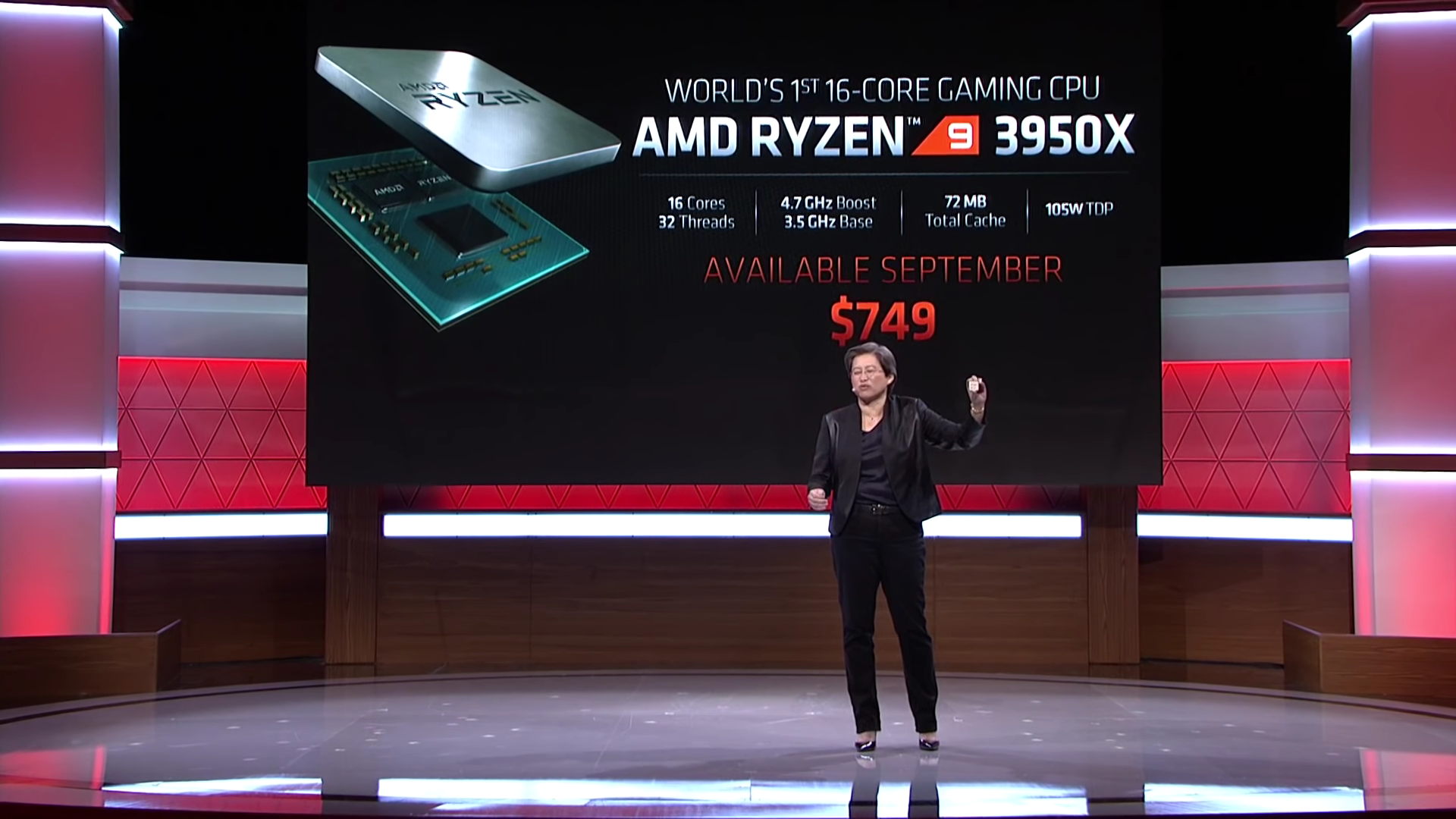
AMD, in the first half of 2019, unveiled their best product line to date. With the cache (both CPU cache and market cache actually) Ryzen CPU’s had been gaining, AMD’s absence was soon reversing itself into near ubiquity in discussions about CPU’s and computers in general. This came to a head with the launch of Zen 2, another promise by AMD to keep making expensive technologies and features they bring to the table, even cheaper and viable on a budget. And this time, it was in 7 nanometres. Intel had soundly been beaten in the race away from 14 nanometres, and AMD’s new process proved itself by providing a performance boost across the board, in every tested metric there was. From their more mainstream (and currently the best-selling CPU worldwide according to PCPartPicker.com) Ryzen 5 3600, to their 2 ultra-high-end Ryzen 9 3950X, providing users with 16 cores on the same platform as a $250 Ryzen 5 3600, which has 6, and their Ryzen Threadripper 3990X, the world’s first consumer-grade/prosumer 64-core CPU, priced at $3990, like the name suggests. AMD CPU’s usually have had higher core counts than Intel CPU’s, but this time, AMD had improved even more on the downside to it: lesser per-core performance due to a lower IPC (Instructions per Clock). It has to be mentioned that neither the 16-core 3950X, or the $500 3900X with 12 cores still did completely beat the 9900K (or the newer 9900KS, because Intel needed to get a newer model with a slight performance boost to seal their narrow lead over the Ryzen 9’s with their i9’s) in gaming performance. But the absolute destruction they were facing in every other metric, including support for faster peripheral interfaces (PCI Express Gen 4.0), was clear. AMD had not just thrown cores, but also extremely good engineering and business strategy at the problem.
AMD在2019年上半年推出了迄今为止最好的产品线。 随着高速缓存(实际上是CPU高速缓存和市场高速缓存)的普及,Ryzen CPU的市场占有率不断提高,AMD的缺席很快使自身在关于CPU和计算机的讨论中几乎无处不在。 Zen 2的发布引起了人们的极大关注,这是AMD的另一项承诺,那就是继续制造昂贵的技术和功能,并使其在预算上更便宜,更可行。 这次是7纳米。 英特尔在超越14纳米的竞赛中被击败,而AMD的新Craft.io通过在所有经过测试的指标中全面提高性能来证明自己。 从更主流(根据PCPartPicker.com,它是目前全球最畅销的CPU)到Ryzen 5 3600,再到其2个超高端Ryzen 9 3950X,它们可以在同一平台上为用户提供16个内核,而价格为250美元的Ryzen 5 3600。 ,它有6个,以及他们的Ryzen Threadripper 3990X,这是世界上第一个消费级/专业级64核CPU,售价为3990美元,顾名思义。 通常,AMD CPU的内核数要高于Intel CPU,但是这一次,AMD的缺点有所改善:由于IPC(每时钟指令数)降低,单核性能下降。 必须指出的是,无论是16核3950X还是500美元的12核3900X都没有完全击败9900K(或较新的9900KS,因为英特尔需要获得性能稍有提升的新机型以缩小领先优势)比Ryzen 9和i9的游戏性能更高。 但是他们在其他所有指标中都面临着绝对的破坏,包括对更快的外围设备接口(PCI Express Gen 4.0)的支持。 AMD不仅抛弃了内核,而且还解决了这个问题上极好的工程和业务策略。
英特尔的10纳米,英特尔的14纳米,英特尔的7纳米甚至英特尔的22纳米 (Intel’s 10 nm, and Intel’s 14 nm and Intel’s 7 nm and even Intel’s 22 nm)
Can’t catch a break, can they?
不能休息一下,可以吗?
Intel has had troubles in their 14 nm production for a long time. These could be seen having their effects shown on the limited availability of 14 nm CPU’s from the start, but this was particularly exacerbated by 2018, when they actually moved back to their older 22 nm process to manufacture lower-end motherboard chipsets. The bottleneck was not just the R&D of 10 nm all this time, but also a lack of proper supply of 14 nm silicon. That was not the only time we saw 22 nm make a cameo appearance in Intel’s line-up either. Intel had been producing the Pentium G3240 which was based on 22 nm Haswell until 2019, when it was scheduled for discontinuation. But Intel overrode that with a notification on 5th December 2019, as they had to make up for the short supply of entry-level CPU’s in smaller PC’s called NUC’s and to fulfil orders placed by PC manufacturers. It is to be noted that there are Pentium CPU’s that are manufactured on the 14nm (or 14nm+) nodes, which are roughly the same price as this CPU, at least retail, but they are frequently in short supply since 2017, and also tend to be marked up higher in price due to this shortage.
英特尔在14纳米生产中遇到了麻烦。 从一开始就可以看到它们对14 nm CPU的有限可用性产生了影响,但是到2018年,当他们实际上又回到了较早的22 nmCraft.io来制造低端主板芯片组时,这种情况尤其恶化了。 瓶颈不仅一直是10纳米的研发,而且还缺乏14纳米硅的适当供应。 这也不是我们唯一一次看到22 nm出现在英特尔产品线中的亮点。 英特尔一直在生产基于奔腾G3240的奔腾G3240,直到2019年,该奔腾G3240计划于2019年停产。 但是英特尔在2019年12月5日发出通知,以此来弥补这一点,因为他们必须弥补称为NUC的小型PC的入门级CPU的短缺,并履行PC制造商的订单。 值得注意的是,有些奔腾CPU在14nm(或14nm +)节点上制造,与该CPU的价格大致相同,至少是零售价,但自2017年以来它们经常供不应求,而且往往由于这种短缺,价格会上涨。

By May 2018, Intel had 10 nanometre silicon out on sale, but their outputs were very low, and they were only laptop CPU’s, named Cannon Lake. Cannon Lake holds the dubious honour of being the shortest-lived x86 CPU microarchitecture till date, as it managed to spawn one single CPU in all its 18 months of existence. The reason for this was just poor 10 nm yields Intel had to sort out before becoming even a little bit ambitious with 10 nm.
到2018年5月,英特尔售出了10纳米硅,但它们的产量非常低,它们只是笔记本电脑的CPU,名为Cannon Lake。 Cannon Lake一直是迄今为止寿命最短的x86 CPU微体系结构,这令人怀疑,因为它在存在的18个月中都设法产生了一个CPU。 造成这种情况的原因是10纳米成品率很差,英特尔不得不对10纳米一点点野心勃勃。
The other new mention here is Intel’s potential attempt at 7 nanometres. Now, this process, due to differences in fundamental designs and marketing buzzwords, is comparable in terms of evolution to AMD’s next step, to 5 nanometres. 7 nm was in development for a while at Intel, but Intel previously had been rather secretive about its progress and development, although it was scheduled for volume production by 2021 until recently, which was already after a previous announcement of another delay. And then on the 23rd of July, Intel presented their second quarter earnings report of 2020, where yet another 6-month delay was announced. Now the first 7 nm consumer CPU’s could only arrive by the end of 2022 or early 2023. Yet again, Intel had a roadblock ahead of it, in their long process towards a more efficient process. Intel’s stock after that announcement plummeted, as is understandable, by around 16%. How significant was that delay for Intel, and why?
另一个新提及的是英特尔潜在的7纳米尝试。 现在,由于基本设计和营销流行语的不同,该过程在演进方面可与AMD的下一步相媲美,达到5纳米。 英特尔在开发7 nm芯片已有一段时间了,但是英特尔以前一直对其进展和开发保密,尽管它原定于2021年实现批量生产,直到最近才发布,但之前已经宣布再次推迟。 然后在7月23日,英特尔发布了2020年第二季度收益报告,并宣布了又六个月的延期。 现在,首批7 nm消费类CPU只能在2022年底或2023年初问世。再次,英特尔在前进到更高效率的漫长过程中遇到了障碍。 可以理解的是,宣布这一消息后,英特尔的股价暴跌了约16%。 延迟对英特尔有多重要?为什么?
The 7 nm process could have served as the next step after 14 nm, so that Intel could step off of the troubled 10 nm node quickly, and stay with 7nm for long, while resuming the Process-Architecture-Optimisation cadence once again, had it not been delayed completely.
7纳米制程本可以用作14纳米制程之后的下一步,以便英特尔可以Swift摆脱陷入困境的10纳米节点,并长时间停留在7纳米制程,同时再次恢复制程架构最佳化的节奏。没有完全延迟。
We are seeing an approximate six-month shift in our seven-nanometer-based CPU product timing relative to prior expectations. The primary driver is the yield of our seven-nanometer process, which, based on recent data, is now trending approximately 12 months behind our internal target. We have identified a defect mode in our seven-nanometer process that resulted in yield degradation. We’ve root caused the issue, and believe there are no fundamental roadblocks.
我们看到,基于七纳米的CPU产品时序相对于先前的预期大约有六个月的变化。 主要驱动力是我们的七纳米Craft.io的产量,根据最新数据,现在的趋势比我们的内部目标低了约12个月。 我们在七纳米Craft.io中发现了一种缺陷模式,该缺陷模式导致了产量下降。 我们已从根本上解决了问题,并认为没有根本性的障碍。
-Bob Swan, Intel CEO, “Intel (INTC) Q2 2020 Earnings Call Transcript” (From: The Motley Fool)
-英特尔首席执行官鲍勃·斯旺(Bob Swan),“英特尔(INTC)2020年第二季度收益通话记录”(摘自: The Motley Fool )
目前的英特尔 (Intel at present)

In the wake of the announcement of the 7 nm delay, Intel also announced that they will be restructuring their Technology, Systems Architecture and Client Group (TSCG), a major arm led by Intel’s erstwhile Chief Engineering Officer into 5 divisions, all being led by other Intel staff while directly reporting to CEO Bob Swan. The Chief Engineering Officer position would then be vacated as Murthy Renduchintala, the executive at that position, had been let go. This comes with the stock hit Intel received after the announcement, as well as a potential class-action lawsuit that their investors have gone forward with, claiming that the defendant willingly concealed information about the issues with the 7 nm node under development from investors. In addition to the lawsuit, the restructuring and the stock price fall, Intel still has to resolve their development of the “defect mode” that their 7 nm node had that led to this issue in the first place.
在宣布7纳米延迟之后,英特尔还宣布将重组其技术,系统架构和客户组(TSCG),这是由英特尔前任首席工程官领导的主要部门,分为5个部门,所有部门均由英特尔领导。其他英特尔员工,同时直接向首席执行官Bob Swan汇报。 由于该职位的高管Murthy Renduchintala已被放任,因此首席工程官职位将被撤职。 公告发布后,英特尔收到了热卖的股票,以及投资者提出的潜在集体诉讼,声称被告愿意向投资者隐瞒有关正在开发的7 nm节点问题的信息。 除了诉讼,重组和股价下跌之外,英特尔仍然必须解决他们的7 nm节点导致这种问题的“缺陷模式”的发展。
Additionally, Intel also announced that they will seek the help of third-party CPU manufacturers to facilitate the development and production of their 7 nm silicon, such as TSMC, who also manufacture AMD and Apple processors. TSMC’s and Intel’s partnership has been dubbed as a “rescue” for Intel, by TSMC themselves, instead of a “normal” collaboration.
此外,英特尔还宣布,他们将寻求第三方CPU制造商的帮助,以促进他们7纳米芯片的开发和生产,例如台积电(TSMC),后者也生产AMD和Apple处理器。 台积电本身将台积电和英特尔的伙伴关系称为英特尔的“营救”,而不是“正常”的合作。
Intel does seem to be finally moving on in consumer CPU’s though, for the end of 2020. The “11th Generation” desktop CPU’s, due to be announced in September called Tiger Lake is rumoured to be on a 10 nm process, like their Tiger Lake laptop CPU’s which released in late 2019. We shall only know by September, however.
不过,英特尔似乎确实终于在2020年底前在消费类CPU方面取得了进展。有传言称将于9月份发布的“第11代”台式机CPU,称为Tiger Lake ,就像他们的Tiger Lake一样,采用10 nmCraft.io。笔记本电脑的CPU在2019年末发布。但是,我们只能在9月之前知道。
结论 (Conclusion)
Intel still is in no deep trouble. Their incredibly diverse portfolio is a fantastic risk-mitigating strategy for their CPU R&D, making them enough profits to sustain perhaps even more such delays and lawsuits. They did try their best to be competitive with all the problems hounding them, by maximising the potential out of both 14 nm and their marketing strategy departments, but it is clear that Intel’s CPUs have been under great scrutiny and reasonable criticism, and it is about time Intel comes up with enough of a justification for why they are the best CPU makers in the world, as that title seems to be under challenge by AMD at present.
英特尔仍然没有什么大麻烦。 他们令人难以置信的多样化投资组合对于他们的CPU研发而言是一种绝妙的风险减轻策略,使他们有足够的利润来承受甚至更多的此类延误和诉讼。 他们尽了最大的努力,通过最大化14 nm及其市场营销部门的潜力来解决所有困扰他们的问题,但是很明显,英特尔的CPU受到了严格的审查和合理的批评,这是关于英特尔提出了足够的理由说明为什么它们是世界上最好的CPU制造商,因为该称号目前正受到AMD的挑战。
翻译自: https://medium.com/swlh/intels-troubles-in-shrinking-down-93e88a4b8efc
英特尔 英特尔 显示器音频


 73
73

 被折叠的 条评论
为什么被折叠?
被折叠的 条评论
为什么被折叠?
 到【灌水乐园】发言


