


前言
本篇主要介绍该IP核的“使用”,和实际项目工程,为下一篇的设计和板上调试做做准备工作,这个“使用”可不像BRAM、DSP核那么简单了,使用的过程中还是有很多坑要踩的;主要参考是该核的手册pg047,代码来源于生成的Example,不同的器件和软件版本可能会有差异,但影响不大。时间充裕的话,建议将整个文档都过一下,把官方的仿真跑一遍,不然,有可能会像我刚开始一样,因为理解不够,出现一些天真的想法。
工程简介
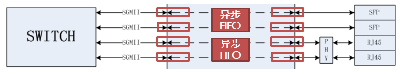
要做的事情是FPGA内部完成“(Bridge)桥梁”的作用,一方面通过PHY或者光模块将电口和光口的串行数据转换成并行,另一方面再将FPGA解析出的数据以SGMII总线发送给交换芯片,重点在跨时钟域处理和自协商内部的逻辑需要自己设计,为了脱敏,本篇不提供完整代码,主要放在思路和避坑。
前端IP核例化
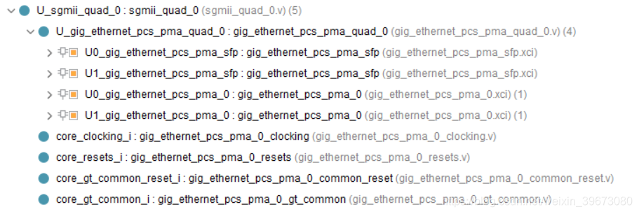
光口与电口端,命名为Q0吧
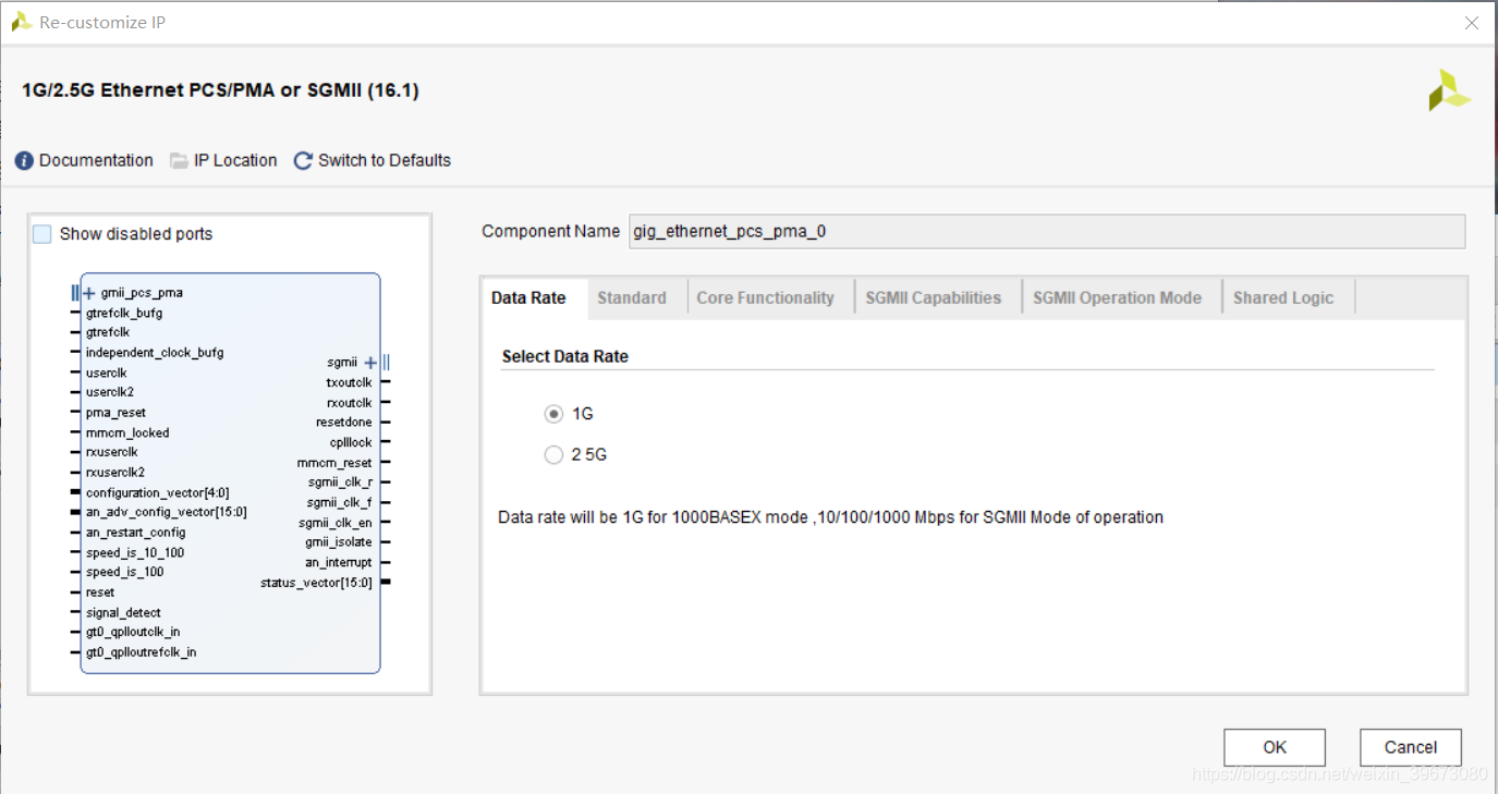
速率和模式
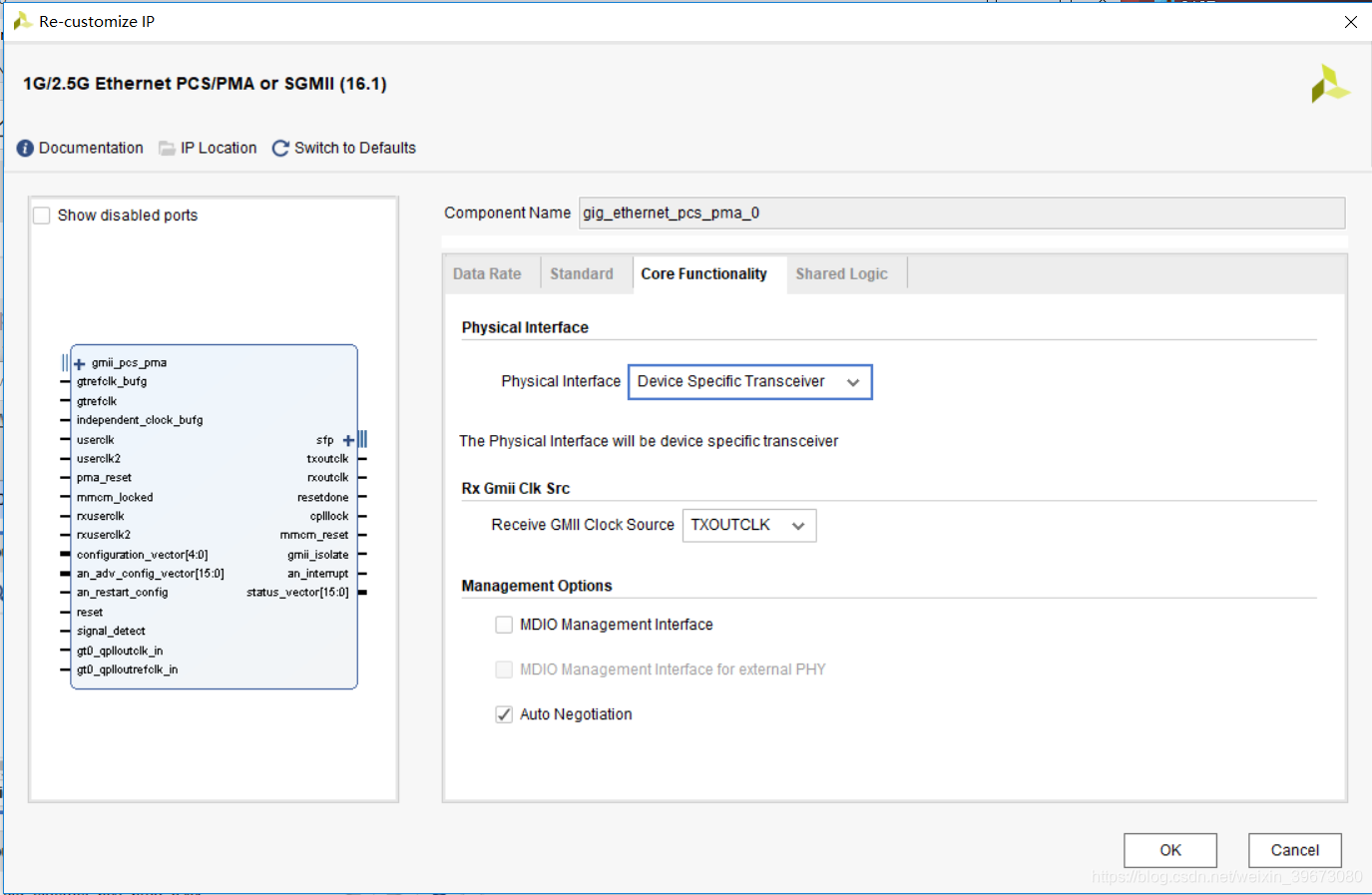
从IP核的名字可以看出,该核通过配置可以生成两种核,光口可以用以太网PCS/PMA mode,电口具有PHY采用SGMII mode,这里速率采用1G,因为其内部有8b/10b转换,所以参考时钟则是125MHz,有效的数据传输速率就变成了125*10*8/10,备选项如果勾选,IP核就会把底层SerDes的一些寄存器接口引出来供用户配置,这里不需要。
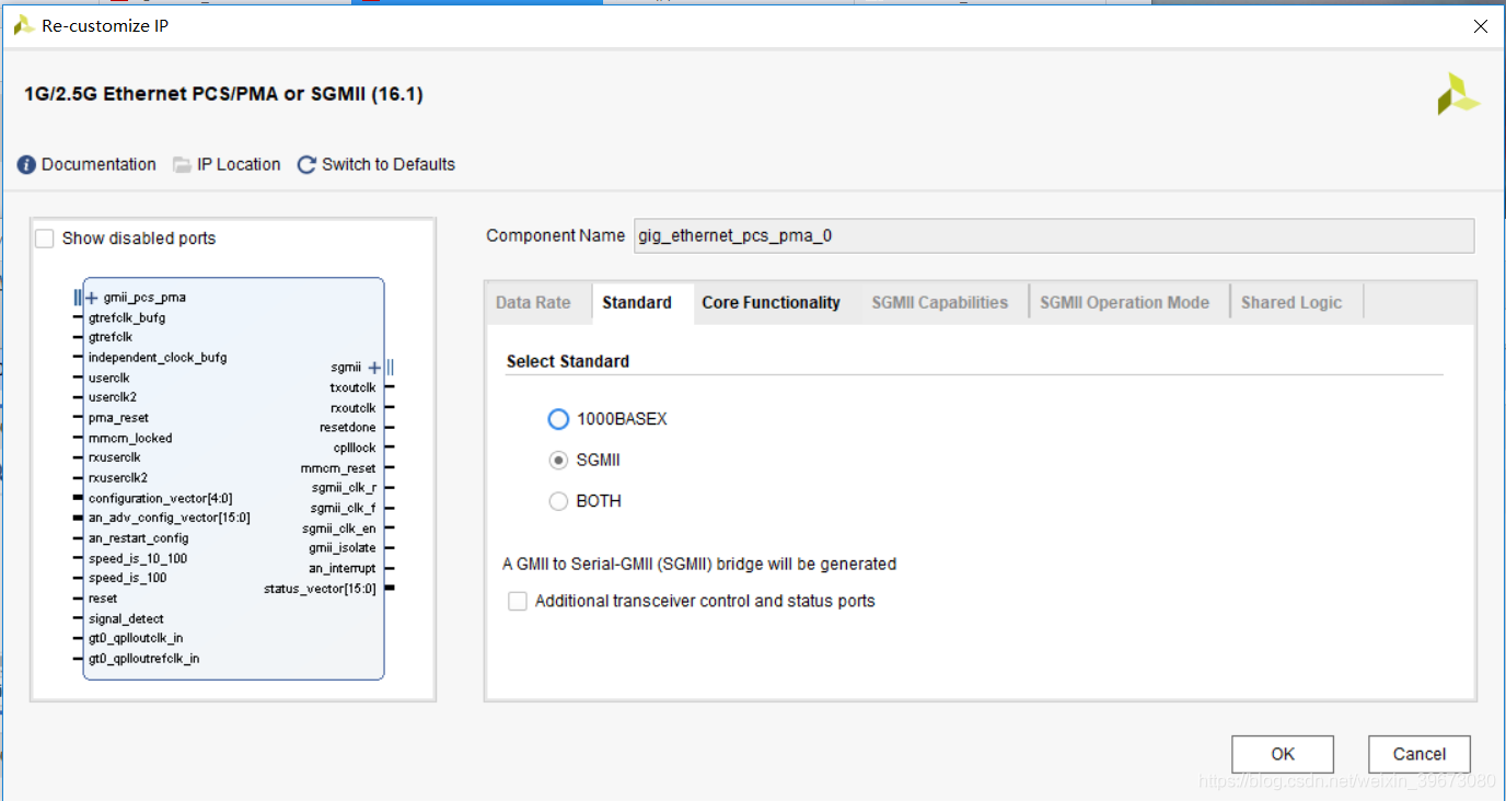
SGMII mode
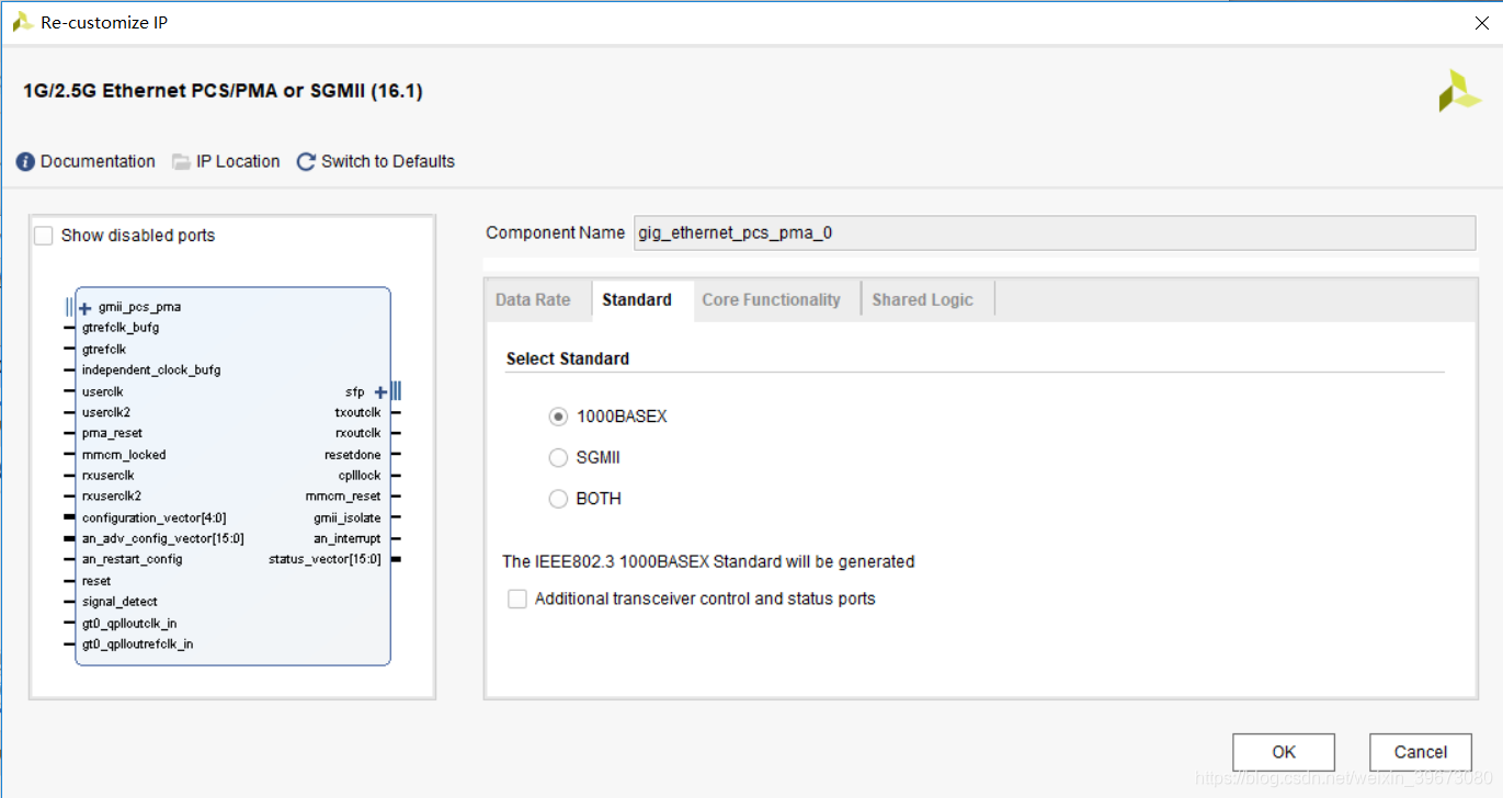
1000BASEX mode
核配置
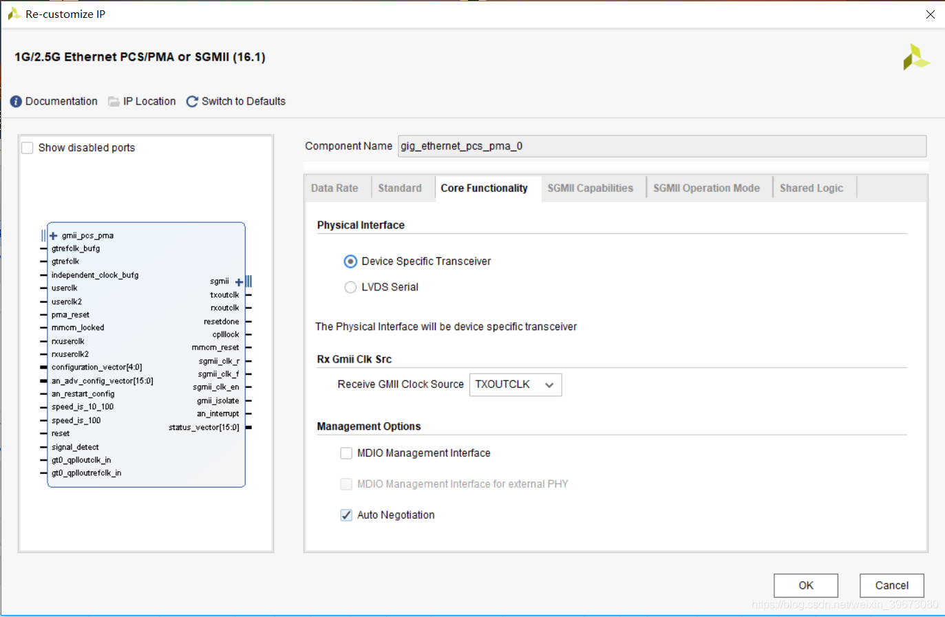
1000BASEX的核配置就简单的多了,因为必须要使用到PCS和PMA,因此物理接口必选device specific TR,然后是GMII解析出来的时钟选择,自协商功能勾选,MDIO是一种配置IP核的总线,有时钟、数据、标志信号和中断,我的感觉是提供给CPU用的,给上层提供一个方便的配置管理接口;对于FPGA呢,可以采用另一种途径,Configuration Register,通过寄存器的形式去完成配置,虽然FPGA也能利用MDIO总线,总归是麻烦了些,所以就只用默认的寄存器配置途径。
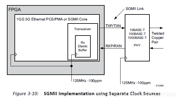
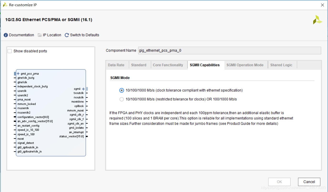
SGMII模式除了可以用TR,还可以用LVDS接口;PHY与FPGA跨时钟的BUFFER选项,这个看手册Figure 3-10;
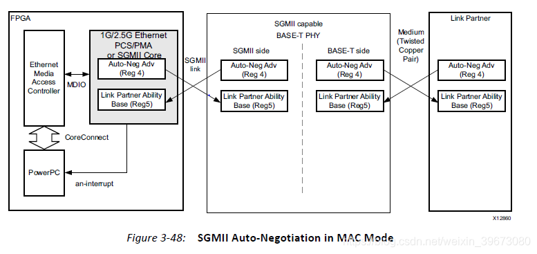
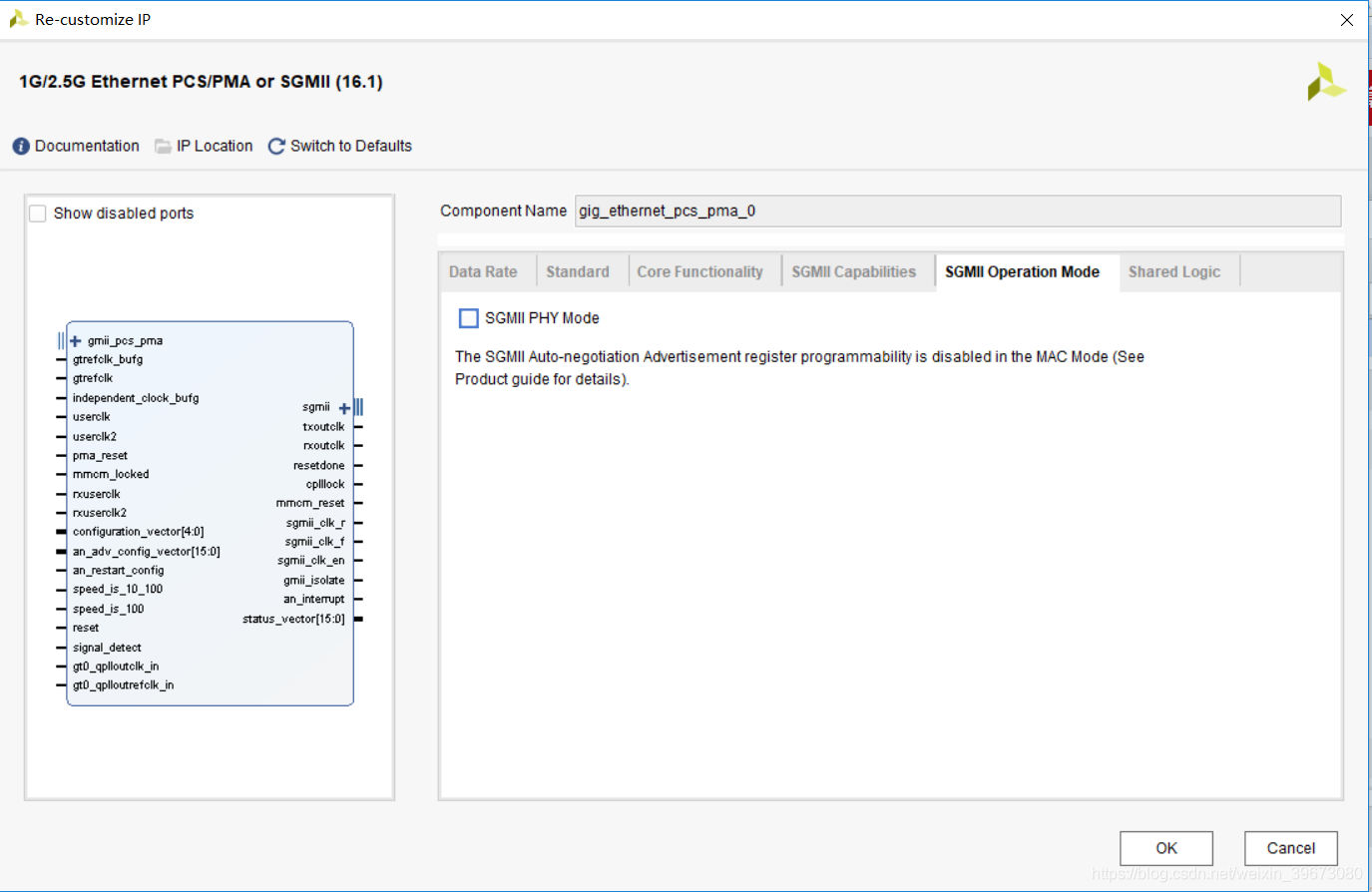
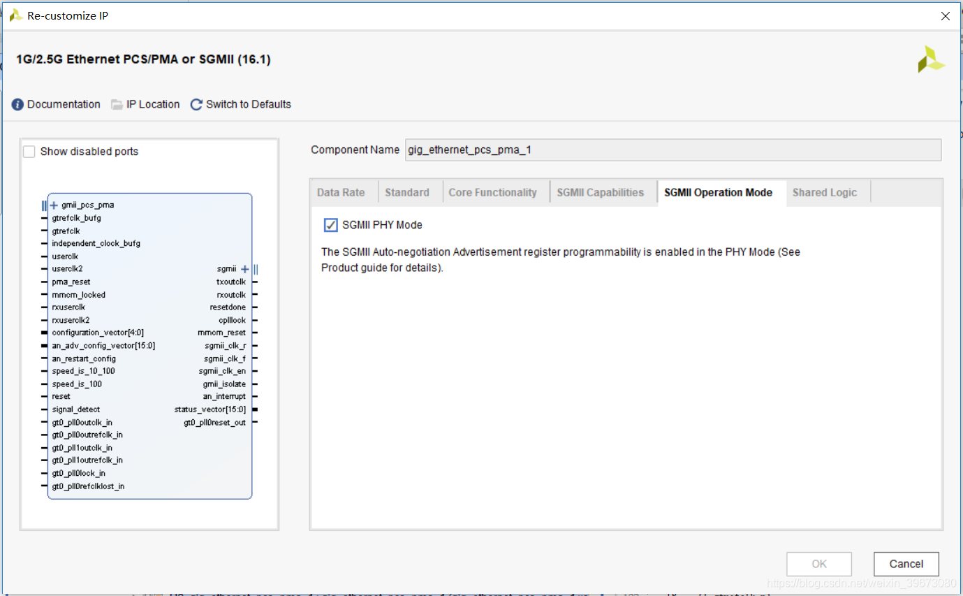
还有工作模式选项,默认MAC mode,勾选PHY mode,这个对自协商功能来说非常重要,因为,只有PHY mode,自协商广播寄存器是可写的(Advertisement register is programmable),按照我的理解就是,MAC模式中的速率、双工、流控等信息只能从对端获取,PHY模式则可以通知对端自己的配置信息;关于自协商的数据过程,SGMII mode和1000BASEX mode比较类似,都是通过协议里的两个寄存器reg4、reg5交叉式的通知与获取,当然,并不是像图中那样还有专门的连线,自协商信息也是通过SGMII总线收发的,抓status vector的信号就可以看到协议里/C/码形式的,bit2代表的自协商配置信息流(AN CONFIG Sequences),总之呢,前端选择默认模式就好,但后端一定要选择PHY mode,因为它必须把自协商信息广播(advertise)给交换芯片的reg5

1000BASEX mode
SGMII mode
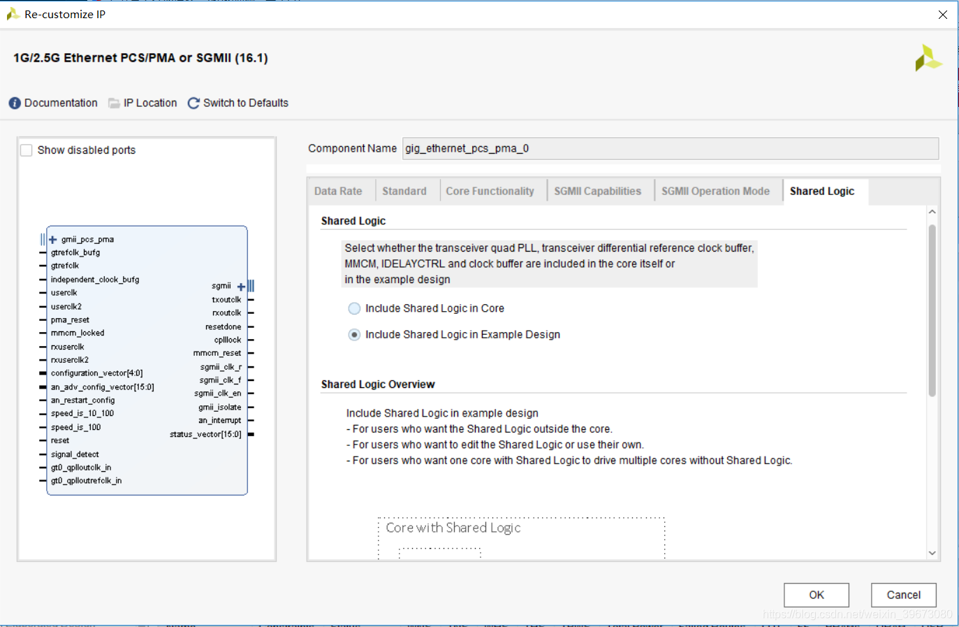
Shared Logic
Xilinx很贴心,它把所需要的外围电路都设计好了,主要包括时钟管理和复位的一些逻辑,in Core表示它会把这些逻辑封装进核里,成为一个新核,把处理后的接口引出来;in Example design则是会像例子里的一样,外围电路以独立模块的形式呈现;举个例子,in Example design模式里MMCM会将时钟锁定信息输入到核的mmcm_locked,而在in Core模式,只能看到mmcm_locked_out,模块间的逻辑因为进一步封装而被隐藏了。
因为,需要用它来加速工程开发,并不意味着不要要看它的代码和手册,这里面也有坑,比如,它的异步复位是高有效。
Q0模块接口
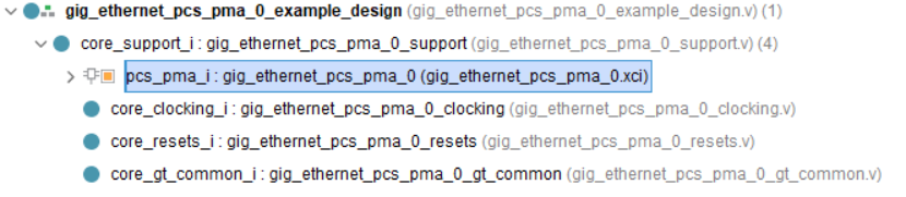
例子中,顶层gig_ethernet_pcs_pma_0_example_design对包括核和外围电路的例化模块core_support_i又进行了一次封装
顶层模块接口为以下代码,注释很详细,例子是为了收发演示用的,实际中肯定要对这个例子进行修改,主要是删除例子中不需要的逻辑,增加一些接口,并且对并列的核进行一次封装。
module gig_ethernet_pcs_pma_0_example_design
(
// An independent clock source used as the reference clock for an
// IDELAYCTRL (if present) and for the main GT transceiver reset logic.
// This example design assumes that this is of frequency 200MHz.
input independent_clock,
// Tranceiver Interface
//---------------------
input gtrefclk_p, // Differential +ve of reference clock for MGT: very high quality.
input gtrefclk_n, // Differential -ve of reference clock for MGT: very high quality.
output rxuserclk2,
output txp, // Differential +ve of serial transmission from PMA to PMD.
output txn, // Differential -ve of serial transmission from PMA to PMD.
input rxp, // Differential +ve for serial reception from PMD to PMA.
input rxn, // Differential -ve for serial reception from PMD to PMA.
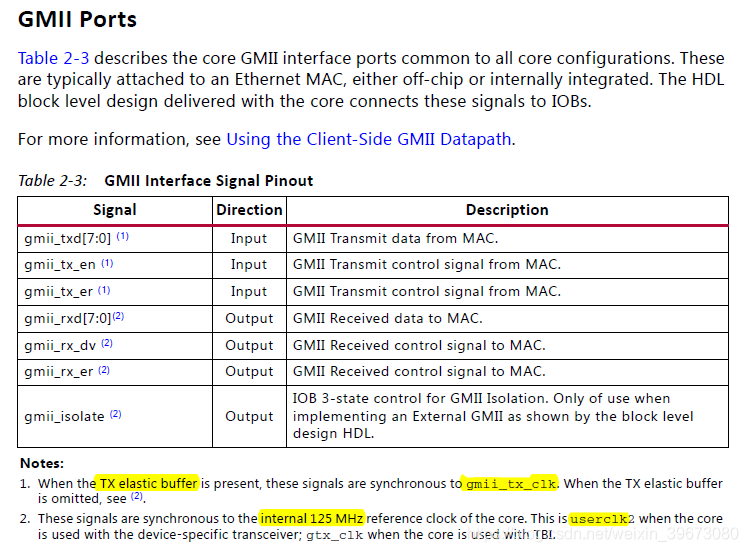
// GMII Interface (client MAC <=> PCS)
//------------------------------------
output sgmii_clk, // Clock for client MAC
input [7:0] gmii_txd, // Transmit data from client MAC.
input gmii_tx_en, // Transmit control signal from client MAC.
input gmii_tx_er, // Transmit control signal from client MAC.
output reg [7:0] gmii_rxd, // Received Data to client MAC.
output reg gmii_rx_dv, // Received control signal to client MAC.
output reg gmii_rx_er, // Received control signal to client MAC.
// Management: Alternative to MDIO Interface
//------------------------------------------
input [4:0] configuration_vector, // Alternative to MDIO interface.
output an_interrupt, // Interrupt to processor to signal that Auto-Negotiation has completed
input [15:0] an_adv_config_vector, // Alternate interface to program REG4 (AN ADV)
input an_restart_config, // Alternate signal to modify AN restart bit in REG0
// Speed Control
//--------------
input speed_is_10_100, // Core should operate at either 10Mbps or 100Mbps speeds
input speed_is_100, // Core should operate at 100Mbps speed
// General IO's
//-------------
output [15:0] status_vector, // Core status.
input reset, // Asynchronous reset for entire core.
input signal_detect // Input from PMD to indicate presence of optical input.
);
工程Q0模块,把两对4个核封装一下,就可以“共用”同一套外围电路了,当然这是加引号的共用
顶层模块代码把4个核的端口都引出来就好,这里特别要注意,也是大坑之一的地方是核的配置接口一定要配置,configuration_vector是用来配置reg0,bit4一定要置1;speed_is虽然是用来配置sgmii_clk_r/f频率的,但它只是一个默认状态下的配置,自协商的速率还是要通过对端reg4发送到核reg5进行配置的,所以,想通过speed_is来自协商还是很天真的,我觉得这也是手册没有讲清楚的地方之一,或许默认用户已经很熟悉协议?
.I_configuration_vector_2        (5'b10000           ),
.I_configuration_valid_2         (1'b0               ),
.O_an_interrupt_2                (                   ),
.I_an_adv_config_vector_2        (16'h21             ),
.I_an_adv_config_val_2           (1'b0               ),
.I_an_restart_config_2           (1'b0               ),

.I_speed_is_10_100_2             (1'b0               ),
.I_speed_is_100_2                (1'b0               ),
.O_sgmii_clk_r_2                 (         			 ),
.O_sgmii_clk_f_2                 (                   ),
另一个大坑是时钟选择,这里强调的是GMII解析出的随路时钟用的是userclk2,原因在于手册上的说明,感觉之所以用不同时钟,就是因为不同的情况,核内部进行了一些时钟域上的处理,最终引出的随路时钟也就随之变化,所以,这个要根据自己的项目实际去决定。
后端IP核例化
核配置
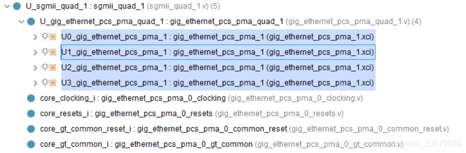
后端命名为Q1吧,它是FPGA内部与交换芯片间的桥梁,所以例化的都是SGMII mode,这里特别强调的是,一定要选PHY mode,因为需要把前端Q0的自协商信息通过Q1的reg4去advertise交换的reg5,这时,交换则是MAC侧。
Q1模块接口
注意与Q0对应就好
这里与Q0不同的就是需要将配置寄存器接口引模块顶部,因为需要根据Q0的status_vector通过an_adv_config_vector去配置reg4,这里的一个坑是自协商的时序,通过MDIO总线需要配合configuration_valid信号,而通过寄存器方式则需要an_restart_config的上升沿,手册里给出了触发自协商的方式,显然,在逻辑内部完成AN触发只能通过an_restart_config信号。
.I_configuration_vector_2        (5'b10000                  ),
.I_configuration_valid_2         (1'b0                      ),
.O_an_interrupt_2                (                          ),
.I_an_adv_config_vector_2        (I_an_adv_config_vector_2  ),
.I_an_adv_config_val_2           (1'b0                      ),
.I_an_restart_config_2           (I_an_restart_config_2     ),
顶层模块
顶层需要解决两个问题,第一、数据同步,Q0与Q1的数据收发都在不同时钟域下,因此每一对都需要两个异步FIFO完成缓存;第二、自协商,Q0侧的自协商信息需要实时的广播给Q1,并完成与交换的自协商。整体工程结构如图
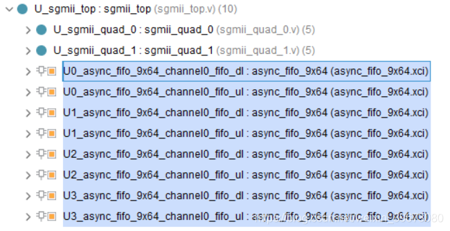
异步FIFO
这里调用的IP核,数据位宽为1+8,最高为是data_valid使能信号,代码片段如下,因为是对称和重复的,看一对的一半注释就明白了
//dl Q1从Q0读出所需要的空标志信号
always@(posedge S_quad1_txuserclk2_out_2)begin
    S_channel2_fifo_dl_empty_d1 <= S_channel2_fifo_dl_empty;
    S_channel2_fifo_dl_empty_d2 <= S_channel2_fifo_dl_empty_d1;
end
//ul Q0从Q1读出所需要的空标志信号
always@(posedge S_quad0_txuserclk2_out_2)begin
    S_channel2_fifo_ul_empty_d1 <= S_channel2_fifo_ul_empty;
    S_channel2_fifo_ul_empty_d2 <= S_channel2_fifo_ul_empty_d1;
end

//dl FIFO
//写使能有效
assign S_channel2_fifo_dl_wr_en = 1'b1;
//写时钟为Q0的解析时钟
assign S_channel2_fifo_dl_wr_clk = S_quad0_txuserclk2_out_2;
assign S_channel2_fifo_dl_din = {S_quad0_gmii_rx_dv_2,S_quad0_gmii_rxd_2[7:0]};
//读使能为Q1时钟域下的非空信号
assign S_channel2_fifo_dl_rd_en = !S_channel2_fifo_dl_empty_d2;
//读时钟为Q1时钟域
assign S_channel2_fifo_dl_rd_clk = S_quad1_txuserclk2_out_2;
assign S_quad1_gmii_tx_en_2 = S_channel2_fifo_dl_dout[8];
assign S_quad1_gmii_txd_2 = S_channel2_fifo_dl_dout[7:0];

assign S_channel2_fifo_ul_wr_en = 1'b1;
assign S_channel2_fifo_ul_wr_clk = S_quad1_txuserclk2_out_2;
assign S_channel2_fifo_ul_din = {S_quad1_gmii_rx_dv_2,S_quad1_gmii_rxd_2[7:0]};
assign S_channel2_fifo_ul_rd_en = !S_channel2_fifo_ul_empty_d2;
assign S_channel2_fifo_ul_rd_clk = S_quad0_txuserclk2_out_2;
assign S_quad0_gmii_tx_en_2 = S_channel2_fifo_ul_dout[8];
assign S_quad0_gmii_txd_2 = S_channel2_fifo_ul_dout[7:0];

async_fifo_9x64 U2_async_fifo_9x64_channel0_fifo_dl
(
.rst            (!I_sys_rst_n                   ),
.wr_en          (S_channel2_fifo_dl_wr_en       ),
.wr_clk         (S_channel2_fifo_dl_wr_clk      ),
.din            (S_channel2_fifo_dl_din         ),
.rd_en          (S_channel2_fifo_dl_rd_en       ),
.rd_clk         (S_channel2_fifo_dl_rd_clk      ),
.dout           (S_channel2_fifo_dl_dout        ),
.full           (S_channel2_fifo_dl_full        ),
.almost_full    (S_channel2_fifo_dl_almost_full ),
.empty          (S_channel2_fifo_dl_empty       ),
.almost_empty   (S_channel2_fifo_dl_almost_empty)
);

async_fifo_9x64 U2_async_fifo_9x64_channel0_fifo_ul
(
.rst            (!I_sys_rst_n                   ),
.wr_en          (S_channel2_fifo_ul_wr_en       ),
.wr_clk         (S_channel2_fifo_ul_wr_clk      ),
.din            (S_channel2_fifo_ul_din         ),
.rd_en          (S_channel2_fifo_ul_rd_en       ),
.rd_clk         (S_channel2_fifo_ul_rd_clk      ),
.dout           (S_channel2_fifo_ul_dout        ),
.full           (S_channel2_fifo_ul_full        ),
.almost_full    (S_channel2_fifo_ul_almost_full ),
.empty          (S_channel2_fifo_ul_empty       ),
.almost_empty   (S_channel2_fifo_ul_almost_empty)
);
自协商
这里是Q0与Q1逻辑内部的自协商过程,主要利用Q0的status_vector去配置Q1的an_configuration_vector,代码片段如下
//Q0与Q1之间自协商的透传
//phy2  S_quad1_txuserclk2_out_2  对应core2

//打拍寄存,q0_phy2_status_vector_reg是进行跨时钟处理,q0_phy2_status_vector_reg_reg是进行状态变化检测
reg [15:0] q0_phy2_status_vector;
reg [15:0] q0_phy2_status_vector_reg;
reg [15:0] q0_phy2_status_vector_reg_reg;

always@(posedge S_quad1_txuserclk2_out_2)begin
	if(!I_sys_rst_n)begin
		q0_phy2_status_vector <= 16'b0;
		q0_phy2_status_vector_reg <= 16'b0;
		q0_phy2_status_vector_reg_reg <= 16'b0;
	end
	else begin
		q0_phy2_status_vector <= S_quad0_status_vector_2;
        q0_phy2_status_vector_reg <= q0_phy2_status_vector;
		q0_phy2_status_vector_reg_reg <= q0_phy2_status_vector_reg;
	end
end


//assign AN_restart = ((q0_phy2_status_vector_reg[7]==q0_phy2_status_vector_reg_reg[7])&&(q0_phy2_status_vector_reg[1]==q0_phy2_status_vector_reg_reg[1])&&(q0_phy2_status_vector_reg[0]==q0_phy2_status_vector_reg_reg[0]))?1'b0:1'b1;
//bit7 表征link up or down  bit1、0代表config complete
(*mark_debug*)reg AN_restart_phy2;

always@(posedge S_quad1_txuserclk2_out_2)begin
	if(!I_sys_rst_n)
		AN_restart_phy2 <= 1'b0;
	else if((q0_phy2_status_vector_reg[7]!=q0_phy2_status_vector_reg_reg[7])||(q0_phy2_status_vector_reg[1]!=q0_phy2_status_vector_reg_reg[1])||(q0_phy2_status_vector_reg[0]!=q0_phy2_status_vector_reg_reg[0]))
		AN_restart_phy2 <= 1'b1;
	else
		AN_restart_phy2 <= 1'b0;
end


//S_an_restart_config_2默认应为0,拉高后须释放
always@(posedge S_quad1_txuserclk2_out_2)begin
	if(!I_sys_rst_n)begin
		S_an_adv_config_vector_2	<=	16'h0;
	    S_an_restart_config_2   	<= 	1'b0;
	end
	else if(q0_phy2_status_vector_reg_reg[7]&&q0_phy2_status_vector_reg_reg[0]&&q0_phy2_status_vector_reg_reg[1])
		case({q0_phy2_status_vector_reg_reg[12],q0_phy2_status_vector_reg_reg[11:10]})  ///duplex , speed
			3'b110:begin ///千兆全
				S_an_adv_config_vector_2 <= 16'h9821;
				if(AN_restart_phy2)
				    S_an_restart_config_2	<= 1'b1;
				    //S_an_restart_config_2	<= 1'b0;
				else
				    S_an_restart_config_2  <= 1'b0;
			end
			3'b101:begin///百兆全
				S_an_adv_config_vector_2 <= 16'h9421;
				if(AN_restart_phy2)
				    S_an_restart_config_2	<= 1'b1;
                	//S_an_restart_config_2    <= 1'b0;
				 else
				    S_an_restart_config_2 <= 1'b0;
			end
			3'b001:begin///百兆半
				S_an_adv_config_vector_2 <= 16'h8421;
				if(AN_restart_phy2)
				    S_an_restart_config_2	<= 1'b1;
                	//S_an_restart_config_2    <= 1'b0;
                else
                    S_an_restart_config_2 <= 1'b0;
			end
			default:begin
				S_an_adv_config_vector_2 <= 16'h1821;//bit15须设置为0,不然交换一直配置为link up
				S_an_restart_config_2 <= 1'b0;
			end
		endcase
	else begin
	   S_an_restart_config_2<= 1'b0;
	   S_an_adv_config_vector_2 <= 16'h1821;//bit15须设置为0,不然交换一直配置为link up
	end
end
总结
FPGA侧的基本完成了,但是也需要将PHY和交换芯片侧进行配置,因为自协商需要两端都必须AN_enable,否则是不会进行自协商的,下一篇分析抓取的关键信号,最简单粗暴的就是看能不能ping通、有没有丢包。


 7816
7816

 被折叠的 条评论
为什么被折叠?
被折叠的 条评论
为什么被折叠?
 到【灌水乐园】发言


