


- 学习I2C bus
1.电器特性
I2C 是一种使用多主从架构的串行通信总线,作为串行通信协议,I2C 只需要两根线——数据线(SDA)和时钟线(SCL)即可工作,众多主机、从机就是挂载在这两根线上,通过总线上的高低起伏的电平变化进行寻址、握手、仲裁和数据传输等功能,I2C特性如下:
- Only two bus lines are required; a serial data line (SDA) and a serial clock line (SCL).
- SDA :数据信号。这种双向数据信号用于传输或接收所有总线数据。
- SCL :来自主 I2C 的时钟。虽然从设备从不会生成时钟信号,但它能够使时钟保持在低电平的状态,并使总线停顿,直至它准备发送数据或确认/否认(ACK/NACK) 最新数据或地址为止。
- The Master device controls the clock (SCL)
- The slave devices may hold the clock low to prevent data transfer
- No data is transferred unless a clock signal is present
- All slaves are controlled by the master clock
- Each device connected to the bus is software addressable by a unique address and simple master/slave relationships exist at all times; masters can operate as master-transmitters or as master-receivers.
- multi-master bus including collision detection and arbitration to prevent data corruption if two or more masters simultaneously initiate data transfer.
- Serial, 8-bit oriented, bidirectional data transfers rate:
- 100 kbit/s in the Standard-mode
- 400 kbit/s in the Fast-mode
- 1 Mbit/s in Fast-mode Plus
- 3.4 Mbit/s in the High-speed mode.
- Serial, 8-bit oriented, unidirectional data transfers up to 5 Mbit/s in Ultra Fast-mode.
- On-chip filtering rejects spikes on the bus data line to preserve data integrity.
- The number of ICs that can be connected to the same bus is limited only by a maximum bus capacitance.
- I2C所有的数据以位为单位在SDA线上串行传输。
- 同步通信就是通信双方工作在同一个时钟下,一般是通信的A方通过一根CLK信号线传输A自己的时钟给B,B工作在A传输的时钟下。所以同步通信的显著特征就是:通信线中有CLK。
- 非差分。因为I2C通信速率不高,而且通信双方距离很近,所以使用电平信号通信。
- 低速率。I2C一般是用在同一个板子上的2个IC之间的通信,而且用来传输的数据量不大,所以本身通信速率很低。


1.1.开漏结构
SDA 和 SCL 都通过一个电流源或上拉电阻连接到正的电源电压。当总线空闲时,这两条线路都是高电平,连接到总线的器件输出级必须是漏极开路或集电极开路才能执行线与的功能 。
由于开漏输出的的特性,使得总线只受输出端低电平的影响(即设备只能通过输出低电平来使用总线),从而实现了「线与」的功能,即当总线上只要有一个设备输出低电平,整条总线便处于低电平状态,这时候总线被称为占用状态。
1.2.上拉电阻
根据1.1分析,输出端只能输出低电平或高阻态,是不能把总线拉高的,所以需要通过其他方式为总线提供高电平,而上拉电阻就派上用场。当输出端输出高阻态时且没有其他设备拉低总线(即占用总线)时,总线被外部的上拉电阻拉高、呈现出高电平状态。
上拉电阻阻值如何选择?
上拉电阻的大小涉及到通信速率与功耗的取舍,协议层对电平的变化时间有着严格的要求与限制,而电平的变化受总线电气特性的影响。对总线而言,上拉电阻越大,信号的上升时间就越长,通信速率就越低,反之亦然。但电阻也并不是越小越好,阻值过小的话,总线低电平时电阻上的大电流会增加电路的功耗。此外,电容也会影响信号的上升时间,于是就有了 I2C 总线总电容 400 pf 的限制,这直接关系到总线上可挂载设备的数目。
2.I2C寻址
2.1.基本术语

主机和从机都可作为发送器和接收器,每个 I2C 设备有四种工作模式:
- 主发送器
- 主接收器
- 从发送器
- 从接收器
作为一个发送器或接收器由器件的功能决定,如LCD驱动器只是一个接收器, 存储器则既可以接收又可以发送数据。
2.2.总线寻址
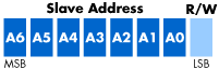
2.2.1. 7Bit Addressing
7位寻址在7位寻址过程中,从机地址在启动信号后的第一个字节开始传输, 字节的前7位为从机地址,第8位为读写位,其中0表示写,1表示读。
保留地址:
I2C规范保留了两组8个地址,1111XXX和0000XXX。这些地址用于特殊用途。
从机地址+R/W	描述
0000 0000	呼叫地址
0000 0001	起始字节
0000 001X	CBUS地址
0000 010X	保留供不同的总线格式
0000 011X	保留将来用
0000 1XXX	HS模式主机码
1111 0XXX	10位从机地址
1111 1XXX	保留将来用
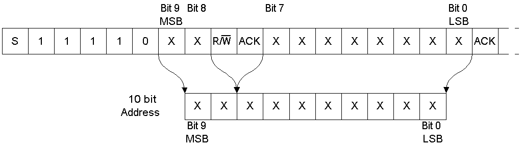
2.2.2.10 Bit Addressing
In order to prevent address clashes, due to the limited range of the 7 bit addresses, a new 10 bit address scheme has been introduced. This enhancement can be mixed with 7 bit addressing and increases the available address range about ten times. After the start condition, a leading ‘11110’ introduces the 10 bit addressing scheme.The last two address bits of the first byte concatenated with the eight bits of the second byte of the whole 10 bit address. Devices which only use 7 bit addressing simply ignore messages with the leading ‘11110’.The following picture shows the first two bytes of a transfer with a 10 bit address.
A master transmitter addresses the slave with two address bytes as described above with the RW-Bit=’0′ followed by data bytes from the master. The master receiver transfer is only possible with a Combined Transfer due to the fact that the second address byte can only be transmitted if the RW-Bit of the first address byte is ‘0’. Hence, the start of a master receiver transfer will be the same as a master transmitter transfer followed by a repeated start condition and the first byte of address byte with RW-Bit=’1′ (switching to slave transmitter mode).
Please refer to the following master receiver sequence:
- Start condition
- First address byte, RW-Bit=’0′, ACK from the slave
- Second address byte, ACK from the slave
- Repeated start condition (no stop condition!)
- First address byte again, RW-Bit=’1′, ACK from the slave, slave switches to transmit mode
- Slave transmits data bytes, ACK from master
- After the last data byte, the master sends a NACK
- Stop condition
2.2.3.How many i2c slaves can a i2c master support?
1>.两个方面限制:
- the address space.
- the total bus capacitance of 400 pF, which restricts practical communication distances to a few meters.
2>.挂载设备数量
7 and 10 bits, which gives a theoretical maximum of 128 and 1024 distinct address, respectively. However, there are a few reserved addresses, such as 0x00 (general call).
3.通信协议
3.1.主、从设备
I2C通信双方地位是不对等的,分主设备和从设备。通信由主设备发起并主导,从设备只是按照协议被动接受,并及时响应。I2C可以设计为单一主设备和多从设备、多主设备或主设备和从设备的组合。主、从之分由通信双方协定(I2C协议并无规定),芯片可以只做主设备、可以只做从设备、也可以既当主设备又当从设备。
主设备负责调度总线,决定某一时间和哪个从设备通信。同一时间只能有一个从设备和主设备通信,其他从设备处于“冬眠”状态。
3.2.Bus Arbitration
Several I2C multi-masters can be connected to the same I2C bus and operate concurrently. By constantly monitoring SDA and SCL for start and stop conditions, they can determine whether the bus is currently idle or not. If the bus is busy, masters delay pending I2C transfers until a stop condition indicates that the bus is free again.
However, it may happen that two masters start a transfer at the same time. During the transfer, the masters constantly monitor SDA and SCL. If one of them detects that SDA is low when it should actually be high, it assumes that another master is active and immediately stops its transfer. This process is called arbitration.
3.2.1.Clock synchronization
The I2C-bus is a multi-master bus. This means that more than one device capable of controlling the bus can be connected to it.
Two masters can begin transmitting on a free bus at the same time and there must be a method for deciding which takes control of the bus and complete its transmission. This is done by clock synchronization and arbitration. In single master systems, clock synchronization and arbitration are not needed.Clock synchronization is performed using the wired-AND connection of I2C interfaces to the SCL line. This means that a HIGH to LOW transition on the SCL line causes the masters concerned to start counting off their LOW period and, once a master clock has gone LOW, it holds the SCL line in that state until the clock HIGH state is reached.

3.3.数据传输
3.3.1.数据的有效性
SDA 线上的数据必须在时钟的高电平周期保持稳定 数据线的高或低电平状态只有在 SCL 线的时钟信号是低电平时才能改变。通过改变 SCL 时钟信号的占空比灵活调整数据的采集和切换时间。

3.3.2.数据传输模式
分为三类:
- 主机发送模式
- 主机接收模式
- 复合模式
3.3.2.1.主机发送模式
在开始数据传输前,主机会发送一个起始信号,紧接着发送目标从机地址,从机被寻址后产生响应信号(响应时钟脉冲由主机产生),接着主机开始发送数据,从机接收数据并产生响应信号,在数据传输完毕时主机发送结束信号,通讯结束。每次数据传输都是始于起始信号止于结束信号,期间总线处于占用状态。
起始、停止信号
起始和停止条件一般由主机产生,总线在起始条件后被认为处于忙的状态;在停止条件的某段时间后总线被认为再次处于空闲状态 。
- Start:SCL 高电平,SDA 由高电平向低电平切换 。
- Stop:SCL 高电平,SDA 由低电平向高电平切换。
- Restart:在通信过程中若要改变目的从机或者数据传输方向,可以不发送结束信号直接再发送一次起始信号,紧接着发送新的从机地址或传输方向,这个起始信号称为「重复起始信号(Sr)」,本质上和普通起始信号相同,但避免了结束、起始信号反复多次发送。在多主机的总线中使用重复起始信号可保持主机对总线的控制权,避免结束信号临时释放总线造成控制权丢失。


如上图所示,在发送完起始信号后,主机紧接着发送一个字节(10 地址模式下两个字节)的地址信息,包括 7 位的从机地址以及一位传输方向控制位,「0」表示发送(写) 「1」表示请求数据(读)。

Acknowledge (ACK) and Not Acknowledge (NACK)
I2C总线上的所有数据都是以8位字节传送的,发送器每发送一个字节,就在时钟脉冲9期间释放数据线,由接收器反馈一个应答信号。应答信号为低电平时,规定为有效应答位(ACK简称应答位),表示接收器已经成功地接收了该字节;应答信号为高电平时,规定为非应答位(NACK),一般表示接收器接收该字节没有成功,对于反馈有效应答位ACK的要求是,接收器在第9个时钟脉冲之前的低电平期间将SDA线拉低,并且确保在该时钟的高电平期间为稳定的低电平。如果接收器是主控器,则在它收到最后一个字节后,发送一个NACK信号,以通知被控发送器结束数据发送,并释放SDA线,以便主控接收器发送一个停止信号P。
- ACK – takes place after every byte. The acknowledge bit allows the receiver to signal the transmitter that the byte was successfully received and another byte may be sent. The master generates all clock pulses, including the acknowledge ninth clock pulse.The transmitter releases the SDA line during the acknowledge clock pulse so the receiver can pull the SDA line LOW and it remains stable LOW during the HIGH period of this clock pulse.
- NACK-- SDA remains HIGH during this ninth clock pulse. The master can then generate either a STOP condition to abort the transfer, or a repeated START condition to start a new transfer. There are five conditions that lead to the generation of a NACK:
- No receiver is present on the bus with the transmitted address so there is no device to respond with an acknowledge.
- The receiver is unable to receive or transmit because it is performing some real-time function and is not ready to start communication with the master.
- During the transfer, the receiver gets data or commands that it does not understand.
- During the transfer, the receiver cannot receive any more data bytes.
- A master-receiver must signal the end of the transfer to the slave transmitter.

3.3.2.2.主机接收模式
在主机接收模式下,同一次通信过程中数据传输只由从机到主机,报文格式如下图:

Master reads slave immediately after first byte. At the moment of the first acknowledge, the master-transmitter becomes a master receiver and the slave-receiver becomes a slave-transmitter. This first acknowledge is still generated by the slave. The master generates subsequent acknowledges. The STOP condition is generated by the master, which sends a not-acknowledge (A) just before the STOP condition.
3.3.2.3.复合模式
主机可以通过重新发送起始信号改变数据传输方向,即同一次通信过程中存在两个数据传输方向,报文格式如下图:

复合模式可以实现主机数据的「先发送后接收」,最典型的应用是通过 I2C 总线控制 EEPROM 读数据 —— 主机(MCU)先发送要读取数据在 EEPROM 内的地址,随后切换模式接收 EEPROM 返回的数据。
4.APB and I2C relationship
This I2C bus controller supports master mode acting as a bridge between AMBA protocol and generic I2C bus system.

- I2C_RF: is used to control the I2C controller operation by the host with APB interface.It implements the register set and the interrupt functionality. The CSR component operates synchronously with the pclk clock.
- I2C_PE: implements the I2C master operation for transmit data to and receive data from other I2C devices. The I2C master controller operates synchronously with the clk_i2c.
- I2C_TOP:is the top module of the I2C controller
5.Txexas board I2C
5.1.Functional Block Diagram

The I2C peripheral consists of the following primary blocks:
- A serial interface: one data pin (I2C_SDA) and one clock pin (I2C_SCL).
- Data registers to temporarily hold receive data and transmit data traveling between the I2C_SDA pin and the CPU or the DMA controller.
- Control and status registers
- A peripheral data bus interface to enable the CPU and the DMA controller to access the I2C peripheral registers.
- A clock synchronizer to synchronize the I2C input clock (from the processor clock generator) and the clock on the I2C_SCL pin, and to synchronize data transfers with masters of different clock speeds.
- A prescaler to divide down the input clock that is driven to the I2C peripheral
- A noise filter on each of the two pins, I2C_SDA and I2C_SCL
- An arbitrator to handle arbitration between the I2C peripheral (when it is a master) and another master
- Interrupt generation logic, so that an interrupt can be sent to the CPU
- DMA event generation logic to send an interrupt to the CPU upon reception or transmission of data
6.韦东山s3c2440

参考资料:
https://www.i2c-bus.org/addressing/10-bit-addressing/
https://rophoenixmakerevolution.files.wordpress.com/2015/09/spi-and-can-bus.pdf
https://www.bluedot.space/tutorials/how-many-devices-can-you-connect-on-i2c-bus/
http://www.ques10.com/p/8794/what-is-bus-arbitration-explain-any-two-techniques/
https://www.totalphase.com/support/articles/200349176-7-bit-8-bit-and-10-bit-I2C-Slave-Addressing


 612
612


 被折叠的 条评论
为什么被折叠?
被折叠的 条评论
为什么被折叠?
 到【灌水乐园】发言


