


- NVIDIA ORIN GPIO
- NVIDIA Xavier GPIO
1.NVIDIA ORIN GPIO
Identifying the GPIO Number
If you designed your own carrier board, to translate from SOM connector pins to actual GPIO numbers, you must understand the following GPIO mapping formula. The translated GPIO numbers can be controlled by the driver.
Because the Jetson module dynamically registers GPIOs, search the kernel messages to check the GPIO allocation ranges for each GPIO group. The command and resulting output are similar to the following:
root@jetson:/home/ubuntu# **dmesg** | **grep gpiochip**
[    5.726492] gpiochip0: registered GPIOs 348 to 511 on **tegra234-gpio**
[    5.732478] gpiochip1: registered GPIOs 316 to 347 on **tegra234-gpio-aon**
As shown in the output above, there are two Jetson GPIO ports with different base indices:
- tegra234-gpio, at base index 348
- tegra234-gpio-aon, at base index 316
You can check the GPIO number in one of the following ways:
- Using a calculation.
Before you get started, you need to know how you plan to configure the offset at each available port.
Here is the list of the tegra234 GPIO ports and offset mapping:

-
Search for the pin details from the Orin pinmux table (see Pinmux Changes).
For example SOC_GPIO08, which is GPIO3_PB.00.
-
Identify the port as B and the Pin_offset as 0.
-
Calculate the pin number with the following formula:
base + port_offset + pin_offset -
Verify the following values:
-
The base is 348.
This value comes from the kernel boot log, it is already noted tegra234-gpio, at base index 348. -
port_offset of port B = 8
This value comes from the tegra234 GPIO port and the offset mapping above. -
pin_offset = 0
-
Pin number = 348 + 8 + 0 = 356
-
-
Using Kernel debugfs.
-
Search for the gpio pin in the Jetson AGX Orin pinmux table (see Pinmux Changes).
For example, SOC_GPIO08, which is GPIO3_PB.00. -
Follow the gpio debugfs look up that use the port and offset.
cat /sys/kernel/debug/gpio | grep PB.00 -
The gpio number is mentioned in the first col as gpio-356.
root@jetson:/home/ubuntu# cat /sys/kernel/debug/gpio | grep PB.00 gpio-356 (PB.00)
-
Note:
To use a pin as GPIO, make sure that E_IO_HV field is disabled in corresponding pinmux register of the GPIO pin. You can disable the field 3.3V Tolerance Enable in pinmux spreadsheet and reflash the board with the updated pinmux file.
例如:
Jetson_AGX_Orin_Series_Pinmux_Config_Template_1.8
- 设置H60 the field 3.3V Tolerance Disable
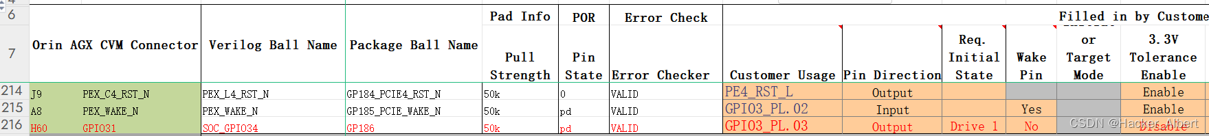
生成的pinmux文件: - nvidia,io-high-voltage = <TEGRA_PIN_DISABLE>;

2.Xavier Linux GPIO
linux/include/dt-bindings/gpio/tegra194-gpio.h

#ifndef _DT_BINDINGS_GPIO_TEGRA194_GPIO_H
#define _DT_BINDINGS_GPIO_TEGRA194_GPIO_H

#include <dt-bindings/gpio/gpio.h>

/* GPIOs implemented by main GPIO controller */
#define TEGRA194_MAIN_GPIO_PORT_A 0
#define TEGRA194_MAIN_GPIO_PORT_B 1
#define TEGRA194_MAIN_GPIO_PORT_C 2
#define TEGRA194_MAIN_GPIO_PORT_D 3
#define TEGRA194_MAIN_GPIO_PORT_E 4
#define TEGRA194_MAIN_GPIO_PORT_F 5
#define TEGRA194_MAIN_GPIO_PORT_G 6
#define TEGRA194_MAIN_GPIO_PORT_H 7
#define TEGRA194_MAIN_GPIO_PORT_I 8
#define TEGRA194_MAIN_GPIO_PORT_J 9
#define TEGRA194_MAIN_GPIO_PORT_K 10
#define TEGRA194_MAIN_GPIO_PORT_L 11
#define TEGRA194_MAIN_GPIO_PORT_M 12
#define TEGRA194_MAIN_GPIO_PORT_N 13
#define TEGRA194_MAIN_GPIO_PORT_O 14
#define TEGRA194_MAIN_GPIO_PORT_P 15
#define TEGRA194_MAIN_GPIO_PORT_Q 16
#define TEGRA194_MAIN_GPIO_PORT_R 17
#define TEGRA194_MAIN_GPIO_PORT_S 18
#define TEGRA194_MAIN_GPIO_PORT_T 19
#define TEGRA194_MAIN_GPIO_PORT_U 20
#define TEGRA194_MAIN_GPIO_PORT_V 21
#define TEGRA194_MAIN_GPIO_PORT_W 22
#define TEGRA194_MAIN_GPIO_PORT_X 23
#define TEGRA194_MAIN_GPIO_PORT_Y 24
#define TEGRA194_MAIN_GPIO_PORT_Z 25
#define TEGRA194_MAIN_GPIO_PORT_FF 26
#define TEGRA194_MAIN_GPIO_PORT_GG 27

#define TEGRA194_MAIN_GPIO(port, offset) \
    ((TEGRA194_MAIN_GPIO_PORT_##port * 8) + offset)

/* GPIOs implemented by AON GPIO controller */
#define TEGRA194_AON_GPIO_PORT_AA 0
#define TEGRA194_AON_GPIO_PORT_BB 1
#define TEGRA194_AON_GPIO_PORT_CC 2
#define TEGRA194_AON_GPIO_PORT_DD 3
#define TEGRA194_AON_GPIO_PORT_EE 4

#define TEGRA194_AON_GPIO(port, offset) \
    ((TEGRA194_AON_GPIO_PORT_##port * 8) + offset)

#endif
基地值:
tegra-gpio, at base index 288
tegra-gpio-aon, at base index 248
查看 Jetson AGX Xavier Pinmux表格, 对应 GPIO3_PZ.03
tegra194-gpio.h定义:
#define TEGRA194_MAIN_GPIO_PORT_Z 25
TEGRA194_MAIN_GPIO, 即tegra-gpio, 基值为288
Linux GPIO计算结果: 25*8 + 288 + 3 = 491
refer to
https://docs.nvidia.com/jetson/archives/r35.1/DeveloperGuide/text/HR/JetsonModuleAdaptationAndBringUp/JetsonAgxOrinSeries.html#pinmux-changes


 6568
6568

 被折叠的 条评论
为什么被折叠?
被折叠的 条评论
为什么被折叠?
 到【灌水乐园】发言


