


目录
这是19年中旬,准备国赛的校赛的时候做的了,
原理图:

PCB:


经过测试,是能够正常使用的。
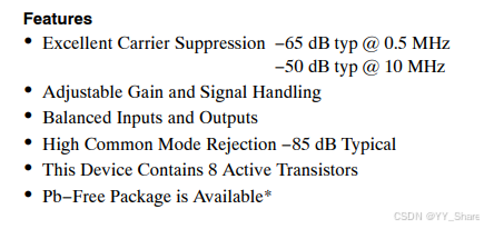
规格
书说明
These devices were designed for use where the output voltage is a product of an input voltage (signal) and a switching function (carrier). Typical applications include suppressed carrier and amplitude modulation, synchronous detection, FM detection, phase detection, and chopper applications.
这些器件设计用于输出电压为a的地方
输入电压(信号)和开关函数(载波)的乘积。
典型的应用包括抑制载波和振幅调制、同步检测、调频检测、相位检测、以及斩波器的应用。
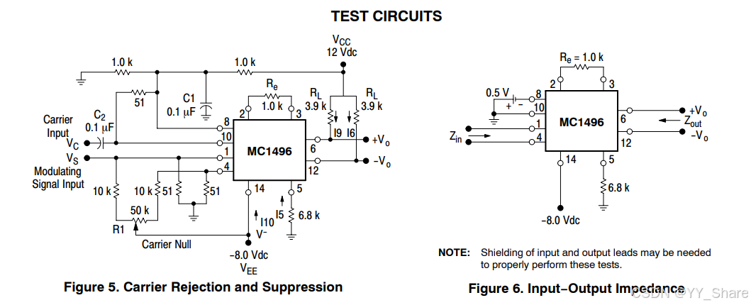
Carrier Feedthrough Carrier feedthrough is defined as the output voltage at carrier frequency with only the carrier applied (signal voltage = 0). Carrier null is achieved by balancing the currents in the differential amplifier by means of a bias trim potentiometer (R1 of Figure 5). Carrier Suppression Carrier suppression is defined as the ratio of each sideband output to carrier output for the carrier and signal voltage levels specified. Carrier suppression is very dependent on carrier input level, as shown in Figure 22. A low value of the carrier does not fully switch the upper switching devices, and results in lower signal gain, hence lower carrier suppression. A higher than optimum carrier level results in unnecessary device and circuit carrier feedthrough, which again degenerates the suppression figure. The MC1496 has been characterized with a 60 mVrms sinewave carrier input signal. This level provides optimum carrier suppression at carrier frequencies in the vicinity of 500 kHz, and is generally recommended for balanced modulator applications. Carrier feedthrough is independent of signal level, VS. Thus carrier suppression can be maximized by operating with large signal levels. However, a linear operating mode must be maintained in the signal−input transistor pair −or harmonics of the modulating signal will be generated and appear in the device output as spurious sidebands of the suppressed carrier. This requirement places an upper limit on input−signal amplitude (see Figure 20). Note also that an optimum carrier level is recommended in Figure 22 for good carrier suppression and minimum spurious sideband generation. At higher frequencies circuit layout is very important in order to minimize carrier feedthrough. Shielding may be necessary in order to prevent capacitive coupling between the carrier input leads and the output leads
翻译:
直通的载体载波馈通定义为输出电压仅应用载波的载波频率(信号电压= 0)。载波零是通过平衡电路中的电流来实现的利用偏置微调电位器的差分放大器(图5中的R1)。载波抑制载波抑制定义为两者的比值边带输出到载波输出为载波和信号指定的电压等级。载波抑制很大程度上依赖于载波输入级别,如图22所示。低价值的载体可以上层开关设备开关不全,导致较低的信号增益,因此较低的载波抑制。一个更高的最佳载波电平导致不必要的设备和电路载波馈通,这又退化了抑制的人物。对MC1496进行了表征以60 mVrms正弦波载波输入信号。这个水平在载波频率下提供最佳载波抑制频率在500千赫左右,通常被推荐用于平衡调制器应用。载波馈通与信号电平VS无关。因此,载波抑制可以通过操作最大化具有大信号电平。然而,线性的工作模式必须维持在信号-输入晶体管对-或调制信号将产生谐波在器件输出中出现为伪边带抑制载波。这个要求设置了一个上限输入-信号幅度(见图20)。还要注意的是如图22所示,建议使用最佳载波级别载波抑制和最小杂散边带
的一代。在较高的频率下,电路布局是非常重要的为了最小化载波馈通。屏蔽可能是为了防止电容之间的耦合是必要的载波输入引线和输出引线。
N The MC1496, a monolithic balanced modulator circuit, is shown in Figure 23. This circuit consists of an upper quad differential amplifier driven by a standard differential amplifier with dual current sources. The output collectors are cross−coupled so that full−wave balanced multiplication of the two input voltages occurs. That is, the output signal is a constant times the product of the two input signals. Mathematical analysis of linear ac signal multiplication indicates that the output spectrum will consist of only the sum and difference of the two input frequencies. Thus, the device may be used as a balanced modulator, doubly balanced mixer, product detector, frequency doubler, and other applications requiring these particular output signal characteristics. The lower differential amplifier has its emitters connected to the package pins so that an external emitter resistance may be used. Also, external load resistors are employed at the device output. Signal Levels The upper quad differential amplifier may be operated either in a linear or a saturated mode. The lower differential amplifier is operated in a linear mode for most applications. For low−level operation at both input ports, the output signal will contain sum and difference frequency components and have an amplitude which is a function of the product of the input signal amplitudes. For high−level operation at the carrier input port and linear operation at the modulating signal port, the output signal will contain sum and difference frequency components of the modulating signal frequency and the fundamental and odd harmonics of the carrier frequency. The output amplitude will be a constant times the modulating signal amplitude. Any amplitude variations in the carrier signal will not appear in the output. The linear signal handling capabilities of a differential amplifier are well defined. With no emitter degeneration, the maximum input voltage for linear operation is approximately 25 mV peak. Since the upper differential amplifier has its emitters internally connected, this voltage applies to the carrier input port for all conditions. Since the lower differential amplifier has provisions for an external emitter resistance, its linear signal handling range may be adjusted by the user. The maximum input voltage for linear operation may be approximated from the following expression: V = (I5) (RE) volts peak. This expression may be used to compute the minimum value of RE for a given input voltage amplitu
MC1496是一种单片平衡调制器电路如图23所示。该电路由上四极差分放大器组成由双电流标准差分放大器驱动来源。输出集热器是交叉耦合的,因此两个输入电压的全波平衡倍增发生。也就是说,输出信号是常数乘以两个输入信号的乘积。线性交流信号乘法的数学分析表示输出频谱仅由和组成和两个输入频率之差。因此,设备可作平衡调制器、双平衡混频器、产品有探测器、倍频器等应用需要这些特殊的输出信号特性。下差分放大器已连接其发射器到封装引脚,以便外部射极电阻可以被使用。此外,外部负载电阻被使用在设备输出。信号的水平可以操作上四极差分放大器线性或饱和模式。下微分放大器在大多数应用中以线性模式工作。对于低电平操作在两个输入端口,输出信号将包含和频和差频分量有一个振幅,它是输入信号幅度的乘积。用于载波输入端口和高电平操作在调制信号口进行线性操作,输出信号将包含和频和差频调制信号频率的分量和载波频率的基次和奇次谐波。输出振幅等于常数乘以调制信号幅度。的振幅变化载波信号不会出现在输出中。
差分的线性信号处理能力放大器定义良好。没有发射极退化线性运行时的最大输入电压为
峰值约为25mv。由于上微分放大器的发射器内部连接,这个电压适用于所有条件下的载波输入端口。由于下差动放大器有一个规定外部发射极电阻,其线性信号处理范围可由用户调整。的最大输入电压线性操作可以用下列公式近似表示表达式:V = (I5) (RE)伏特峰值。这个表达式可以用来计算最小值给定输入电压幅值的反激系数值


 1625
1625

 被折叠的 条评论
为什么被折叠?
被折叠的 条评论
为什么被折叠?
 到【灌水乐园】发言


