


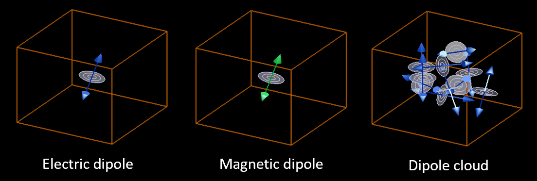
Dipole source - Simulation object
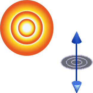 Oscillating dipoles act as sources in Maxwell's equation to produce electromagnetic fields. Dipoles are used to simulate point source radiators, such as radiation from a fluorescent molecule.
In MODE, for the 2.5D FDTD solver, the orientation of the dipole source partially depends on whether the polarization of the propagator simulation is set to TE or TM. Depending on the simulation polarization and dipole type, the theta, phi values may be locked.
General tab
- DIPOLE TYPE: A pull-down menu in which the point source can be configured as an electric dipole (oscillating point charge) or a magnetic dipole (current loop). The radiation pattern of these dipoles is similar, but not exactly the same.
- AMPLITUDE: The amplitude of the point source. The units of the source depend on the dipole type, as explained in the Units and normalization section.
- BASE AMPLITUDE: This is the amplitude that will generate a radiated CW power of 10 nW/m in 2D simulations and 1 fW in 3D simulations.
- TOTAL AMPLITUDE: This is the amplitude actually used in the simulations, it is the product of the AMPLITUDE and the BASE AMPLITUDE.
- PHASE: The phase of the point source, measured in units of degrees. Only useful for setting relative phase delays between multiple radiation sources.
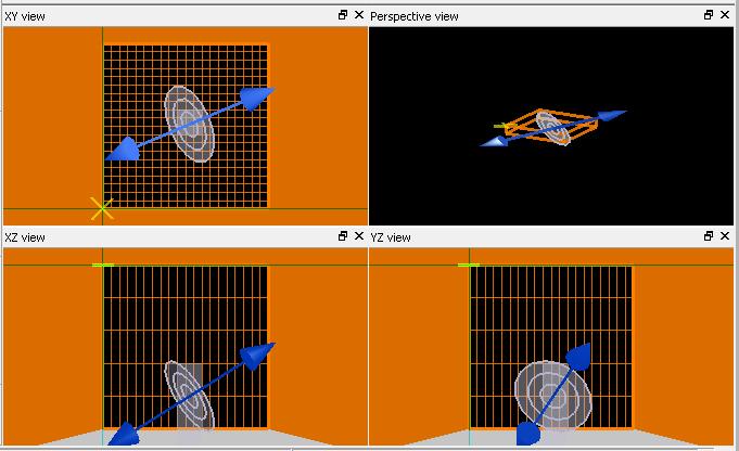
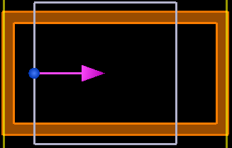
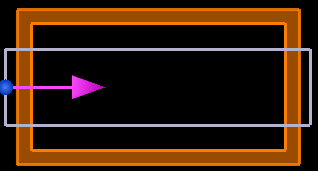
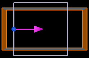
- THETA: The angle with respect to the z-axis of the dipole vector.
- PHI: Angle with respect to the positive x-axis of the dipole vector.
Geometry tab
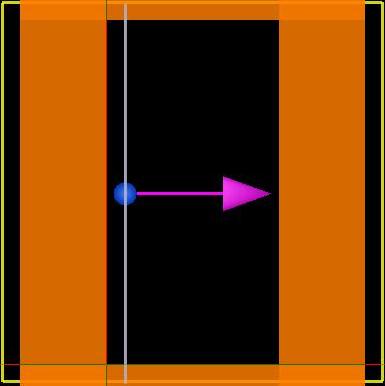
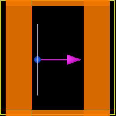
The geometry tab contains options to change the size and location of the sources. The dipole position and direction are specified in terms of the center position and their orientation through angles theta, phi.
Frequency/Wavelength tab
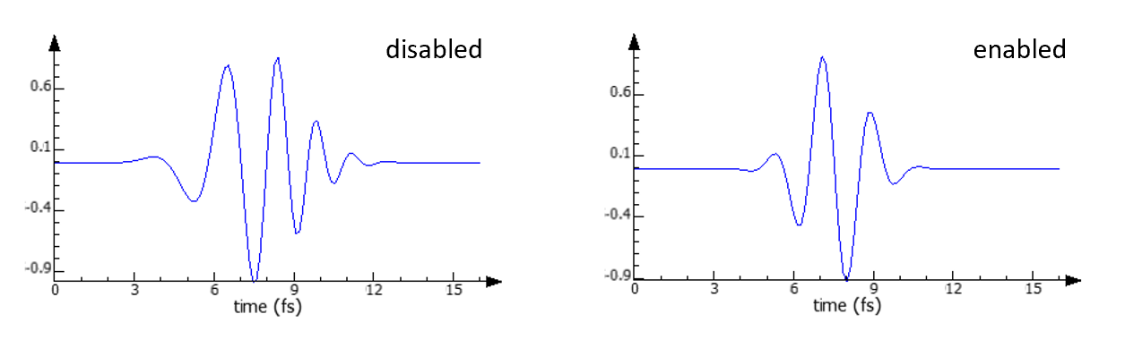
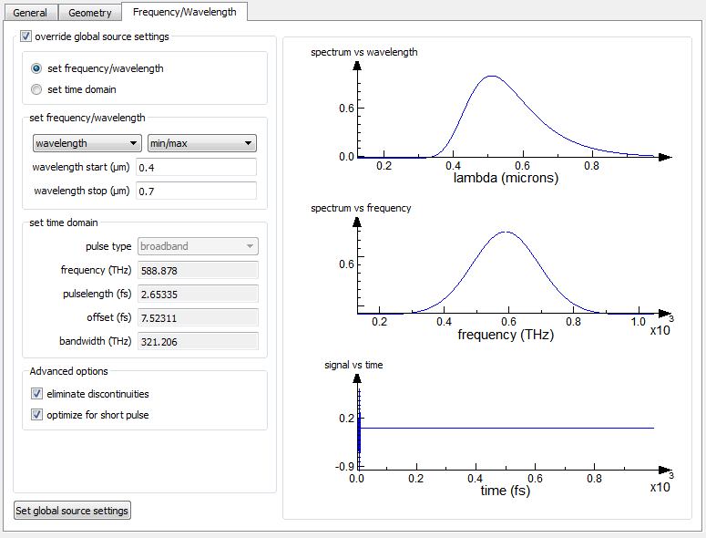
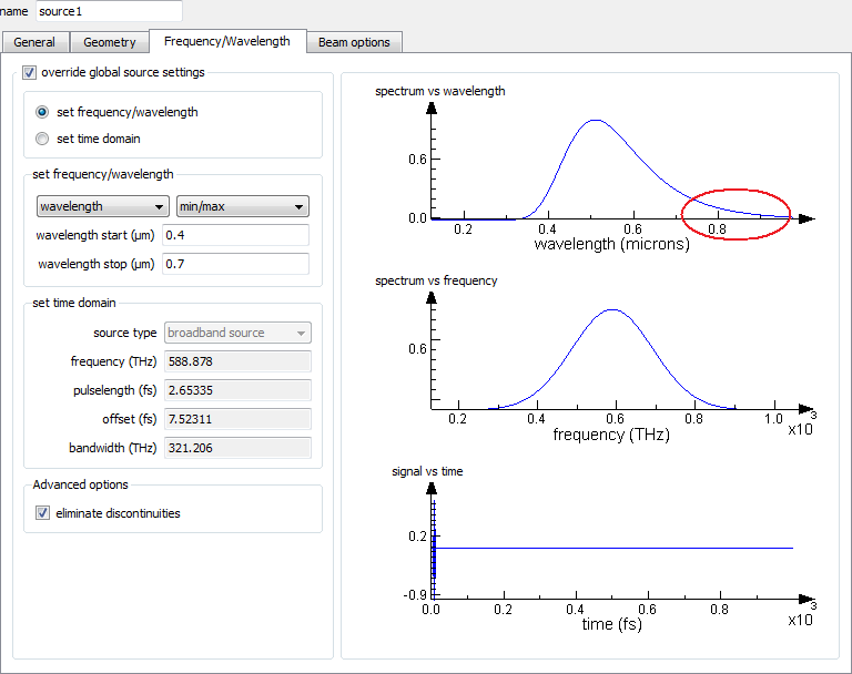
The Frequency/Wavelength tab is shown below. This tab can be accessed through the individual source properties, or the global source properties. Note that the plots on the right-hand side of the window update as the parameters are updated, so that you can easily observe the wavelength (top figure), frequency (middle figure) and temporal (bottom figure) content of the source settings.

At the top-left of the tab, it is possible to chose to either SET FREQUENCY / WAVELENGTH or SET TIME-DOMAIN. In most simulations, the 'SET FREQUENCY / WAVELENGTH ' option is recommended.
If you choose to directly modify the time domain settings, please keep the following points in mind:
- PULSE DURATION: Choose a pulse duration that can accurately span your frequency or wavelength range of interest. However, very short pulses contain many frequency components and therefore disperse quickly. As a result, short pulses require more points per wavelength for accurate simulation.
- PULSE OFFSET: This parameter defines the temporal separation between the start of the simulation and the center of the input pulse. To ensure that the input pulse is not truncated, the pulse offset should be at least 2 times the pulse duration. This will ensure that the frequency distribution around the center frequency of the source is close to symmetrical, and the initial fields are close to zero at the beginning of the simulation.
- SOURCE TYPE: In general, you can choose between ‘standard’ and ‘broadband’ source types. Standard sources consist of a Gaussian pulse at a fixed optical carrier, while the broadband sources consist of a Gaussian pulse with an optical carrier which varies across the pulse envelope. Broadband sources can be used to perform simulations in which wideband frequency data is required – for instance, from 200 to 1000 THz. This type of frequency range cannot be accurately simulated using the standard source type.
Set frequency wavelength
If the SET FREQUENCY / WAVELENGTH option was chosen, this section makes it possible to either set the frequency or the wavelength and choose to either set the center and span or the minimum and maximum frequencies of the source.
For single frequency simulations, simply set both the min and max wavelengths to the same value.
Set time domain
The options in the time domain section are:
- SOURCE TYPE: This setting is used to specify whether the source is a standard source or a broadband source. The standard source consists of an optical carrier with a fixed frequency and a Gaussian envelope. The broadband source, which contains a much wider spectrum, consists of a chirped optical carrier with a Gaussian envelope. When the user uses the script function setsourcesignal, this field will be set as "user input".
- FREQUENCY: The center frequency of the optical carrier.
- PULSELENGTH: The full-width at half-maximum (FWHM) power temporal duration of the pulse.
- OFFSET: The time at which the source reaches its peak amplitude, measured relative to the start of the simulation. An offset of N seconds corresponds to a source which reaches its peak amplitude N seconds after the start of the simulation.
- BANDWIDTH: The FWHM frequency width of the time-domain pulse.
For more information, please visit Changing the source bandwidth
Advanced
- ELIMINATE DISCONTINUITY: Ensures the function has a continuous derivative (smooth transitions from/to zero) at the start and end of a user-defined source time signal. Enabled by default.
- OPTIMIZE FOR SHORT PULSE: Use the shortest possible source pulse.
- This option is enabled by default in the FDTD solver. It should only be disabled when it is necessary to minimize the power injected by the source that is outside of the source range (eg. convergence problems related to broadband steep angled injection).
- This option is disabled by default in the varFDTD solver, as it improves the algorithm's numerical stability.
- ELIMINATE DC: Eliminates the DC component by forcing signal symmetry
Manual calculation of the source time signal
As explained above, the 'Standard' source type uses a fixed carrier with a Gaussian envelope. The following script code shows how to calculate the source time signal used by the source.
# calculate standard pulse time signal
frequency  = 300e12;
pulselength = 50e-15;
offset   = 150e-15;

t      = linspace(0,600e-15, 10000);
w_center  = frequency*2*pi;
delta_t   = pulselength/(2*sqrt(log(2)));
pulse = sin( -w_center*(t-offset)) * exp( -(t-offset)^2/2/delta_t^2 );

plot(t*1e12,pulse,"t (fs)","source pulse time signal");
| Note: There are some small differences between the pulse generated by this code and the actual time signal generated by the 'standard' source pulse setting. If you need very precise control over or knowledge of the source time signal, you should create your own Custom time signal. The 'broadband' option is generated with a more complex function. The precise function is not provided. To create your own arbitrary source time signals, see the Custom time signal page. |
Advanced tab
This tab only appears for the dipole source. The tab contains a RECORD LOCAL FIELD checkbox. When checked, the fields around the dipole are saved; this box must be checked in order to use the dipolepower script function.
Results returned
- DIPOLEPOWER: The power injected into the simulation region by a dipole is returned. The units will be in Watts if cw norm is used and Watts/Hertz2 if no norm is used.
- PURCELL: By utilizing the power measurement, the emission rate enhancement of a spontaneous emitter inside a cavity or resonator, the Purcell factor is returned.
- TIME SIGNAL: Time domain signal of the source pulse.
- SPECTRUM: The fourier transform of time signal.
Testing FDTD dipole sources in homogeneous materials
This section describes the power radiated by a dipole in a homogeneous material.
Theoretical power radiated by a dipole in a homogeneous material
The analytic expressions of total radiated power of electric and magnetic dipoles in a homogeneous material of refractive index n, in 2D and 3D are shown in the following table.
| Dipole type | Total radiate power (Watts) | Units |
|---|---|---|
| 2D TM Electric Dipole | P=π2μ04π|→p0|2ω3 |
| [p0] = Cm/m | |
| 2D TE Electric Dipole | P=π4μ04π|→p0|2ω3 |
| [p0] = Cm/m | |
| 3D Electric Dipole | P=μ04πn|→p0|2ω43c |
| [p0] = Cm | |
| 2D TM Magnetic Dipole | P=π4μ04πn2|→m0|2ω3c2 |
| [m0] = Am2/m | |
| 2D TE Magnetic Dipole | P=π2μ04πn2|→m0|2ω3c2 |
| [m0] = Am2/m | |
| 3D Magnetic Dipole | P=μ04πn3|→n0|2ω43c3 |
| [m0] = Am2 |
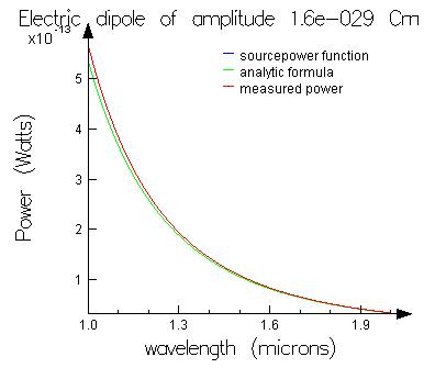
Verifying the emitted power in FDTD.
The script file usr_dipole_power.lsf will compare the above analytic formulas for power radiated by a dipole with the measured results from an FDTD simulation. To run this example, download all three assocated files. Open one of the simulation files (.fsp), then run the script.
The script will run a total of 6 simulations, one for each of the dipole type listed above. In each case, it will compare the total measured power in FDTD/Propagator with the analytic expressions. It does this over a wavelength range of 1 to 2 um. It plots both the measured power and the analytical result for each case. The sourcepower function evaluates the analytic expression described above. The dipolepower function measures the actual power radiated by the dipole.
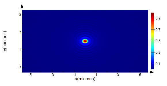
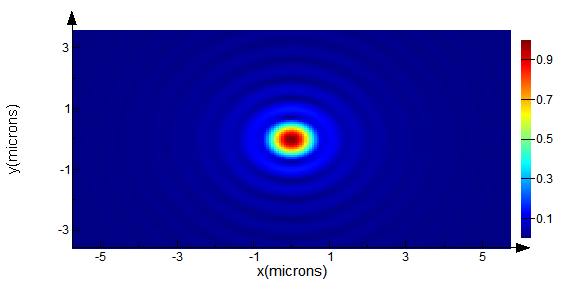
The 3D electric and magnetic dipole comparisons are shown in Figure 1. The percentage difference between the measured result and the analytical expression as a function of points per wavelength in the homogeneous material are shown in Figure 2.

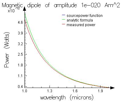
Analytic and measured power for electric and magnetic dipoles.
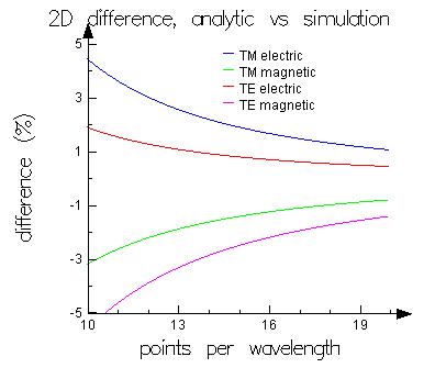
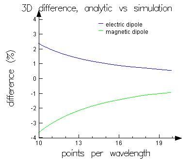
Difference between the analytical power for a dipole and the simulated power in 2D and 3D
(TE/TM and electric/magnetic dipoles).
It is important to understand the following points:
- The main source of the discrepancy is that FDTD is solved on a discrete mesh. The analytic expression comes from a calculation that assumes a continuous homogeneous material instead of a discrete mesh. Therefore it is expected that there is a difference between the simulation and theory which should only go to zero when the mesh size becomes very small.
- In principle, dipole sources are injected by exciting the electric and magnetic fields at only one point on the mesh. In order to allow injection at arbitrary spatial positions and dipole orientations, several mesh points are actually excited with appropriate weighting's. This means that the total injected power changes when you move the dipole by amounts smaller than the mesh size, dx. At 10 points per wavelength, this change in power can be as large as 5% by moving the dipole by dx/2. In Figure 2, the 2D TE electric dipole has the best agreement with the analytic expression compared to the other 2D dipoles, but moving the dipole location by a small amount can make a different dipole type have the best agreement.
We should note that we can compare to the analytic expression for the power radiated from dipoles to within approximately 5% accuracy at 10 points per wavelength. This corresponds to a Mesh Accuracy setting of approximately 2. At 20 points per wavelength (Mesh Accuracy approximately 4-5) the injected power is better than 2%.
The CW normalization option attempts to normalize monitor data to the amount of energy injected into the simulation at each frequency. This allows the user to extract the CW response of a system for a range of frequencies from a single simulation. For this normalization to occur, the injected power must be known. In the case of a dipole, the injected power is calculated from the analytic formula for "total power radiated by a dipole in a homogeneous material".
This means that the simulation data is actually normalized to the amount of power a dipole would inject in a homogenous material, rather than how much power was actually injected into the specific simulation. A dipoles actual injected power can vary significantly from the homogeneous value, depending on what physical structures are near by. Field reflected from nearby structures re-interfere with the source, causing it to inject more or less power than expected. The next section discusses this issue in more detail.
Understanding dipoles in non-homogeneous materials
The actual power emitted by a dipole is highly dependant on the surrounding materials, and can vary significantly from the analytic formula for a dipole in a homogeneous material. This section looks at a specific example of a dipole near a metal wall. In these cases, the CW normalization option will not work correctly because it will normalize data to the analytic formula, rather than the actual power emitted. For accurate power normalization, we must normalize results using the dipolepower function (actual radiated power) rather than the standard sourcepower function (analytic power radiated in homogeneous material).
Normalizing a dipole near a metal wall
In LEDs and OLEDs, the dipoles typically radiate near a metal wall. It is worthwhile to consider power normalization calculations near metal walls.
Open the file usr_dipole_power_metal1.fsp. This structure we are modeling is shown in the following screenshot.
All boundaries are PML, except for the lower z boundary, which is set to metal. There is a single dipole source in the simulation volume. Run the simulation, then paste the following script commands into the script prompt to create the following figures.
f1=c/1.5e-6;
f2=c/1.0e-6;
f=linspace(f1,f2,100);

power1=sourcepower(f,2,"real_source");
power2=dipolepower(f, "real_source"); # actual power radiated by the dipole

plot(c/f*1e6,power1,power2,"wavelength (um)","power");
legend("Analytic power radiated in homogeneous material",
       "Actual power radiated by dipole near metal wall");
plot(c/f*1e6,power2/power1,"wavelength (um)","normalized power");
When the simulation is done, run the script the above commands. They will calculate the total power radiated by the dipole, normalized to the analytic expression for the power radiated by this dipole in a homogeneous material. You'll see the following result shown in the following figure.
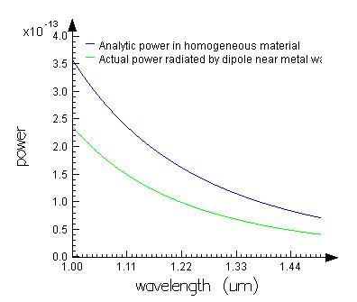
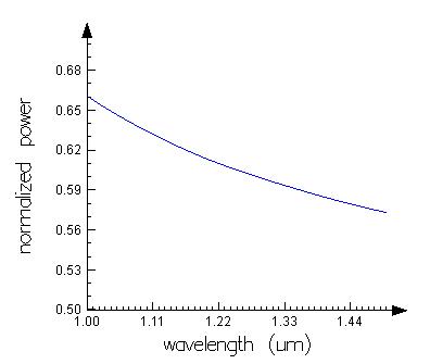
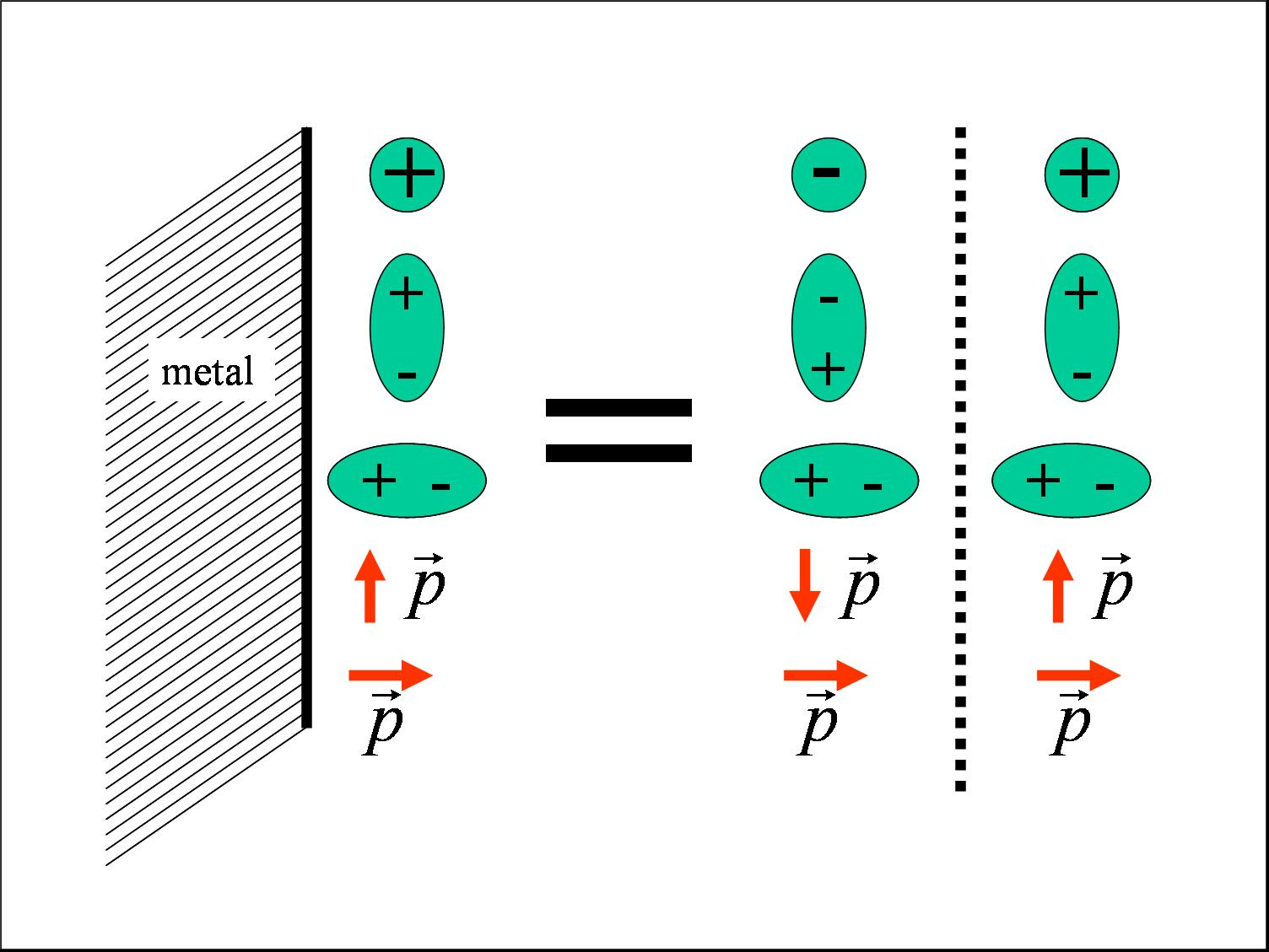
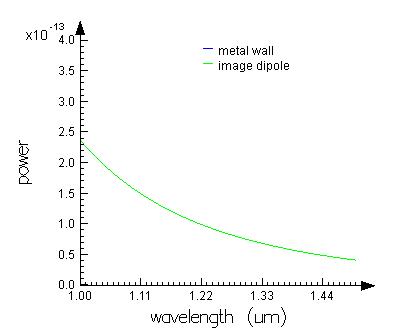
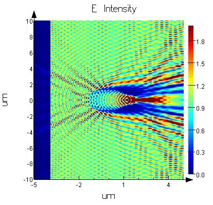
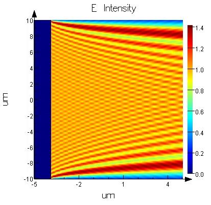
You can see that the radiated power is significantly different than the same dipole in free space. To understand these results, we can consider the equivalent problem to the metal wall. Let’s look at the problem using the method of image charges. The metal wall can be replaced by a dipole with the appropriate orientation at an equal distance behind where the original metal wall was, as shown below:

To simulate this system, load the file usr_dipole_power_metal2.fsp. It is set up with an image charge in place of the metal wall. The lower z boundary has been extended and set to use PML. The dipole source is appropriately positioned. After running the simulation, paste the same script code into the script prompt again. Notice that the figures are exactly the same as the first simulation. In the following figure, the two curves lie on top of one another.
| Note: Dipole radiated power It may seem strange that the total power radiated by the dipole changes when it is near a metal wall, despite the fact that the dipole amplitude is fixed. To understand how this can be, we should realize that a dipole is effectively a small antenna with a fixed current, I |
. The total radiated power is given by P=I2Rrad, where Rrad
| is the radiation resistance of the antenna. By placing the antenna in a different location, we can change the radiation resistance and therefore the total radiated power. Energy is conserved however because the power needed to drive the antenna is different in each case. From the quantum mechanical point of view, which is useful for LEDs, we see that the local density of states is different in free space than it is near a metal wall. This will affect the rate of decay of electron-hole pairs into photons, and can ultimately be used to improve the quantum efficiency. |
| Note: Beam sources As described above, the amount of power radiated by a source can change due to interference with another source, or when it interferes with itself. This is usually only relevant for dipole sources, but it can occur with all types of sources. It is not very important for beam sources because these simulations are usually set up so this interference does not occur. |
Related publications
Barnes, W. L. (1998). Fluorescence near interfaces: The role of photonic mode density. Journal of Modern Optics, 45,661-669. DOI: 10.1080/09500349808230614
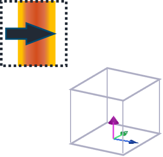
Plane wave and beam source - Simulation object
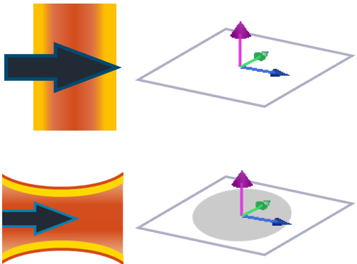 Plane wave sources are used to inject laterally-uniform electromagnetic energy from one side of the source region. In two-dimensional simulations, the plane wave source injects along a line, while in three-dimensional simulations the plane wave source injects along a plane. It is also possible to inject a plane wave at an angle. The plane wave source is actually the same object as the Gaussian source, with the only difference being the SOURCE SHAPE setting. Periodic or Bloch boundary conditions should be used with Bloch/periodic type plane wave source. Diffracting plane wave source can be used with PML in all directions. When a broadband result at angled plane wave incidence is pursued with one simulation without using Bloch BCs, the BFAST source technique should be used, please read more on BFAST plane wave.
A Gaussian source defines a beam of electromagnetic radiation propagating in a specific direction, with the amplitude defined by a Gaussian cross-section of a given width. By default, the Gaussian sources use a scalar beam approximation for the electric field which is valid as long as the waist beam diameter is much larger than the diffraction limit. The scalar approximation assumes that the fields in the direction of propagation are zero. For a highly focused beam, there is also a thin lens source that will inject a fully vectorial beam. The cross-section of this beam will be a Gaussian if the lens is not filled, and will be a since function if the lens is filled. In each case, the beams are injected along a line perpendicular to the propagation direction and are clipped at the edges of the source.
| NOTE: The following changes have been made to the polarization arrows in 2020 R.1.4 to avoid ambiguity with the polarization orientation.
These changes affect only the way the source objects look in the GUI. The simulation results won't be affected in any way. |
General tab
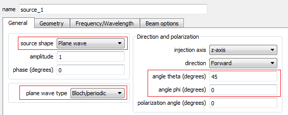
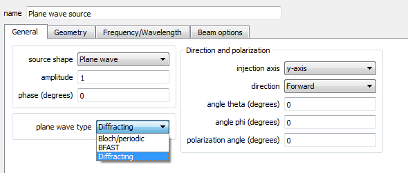
- SOURCE SHAPE: The shape of the beam. It can be changed to a Gaussian, plane wave or Cauchy/Lorentzian.
- AMPLITUDE: The amplitude of the source as explained on the Units and normalization page.
- PHASE: The phase of the point source, measured in units of degrees. Only useful for setting relative phase delays between multiple radiation sources.
- PLANE WAVE TYPE: Sets the type of the plane wave source. More information about each source type is available in dedicated topic available from "See also" section above. This menu is available for plane wave source only.
- INJECTION AXIS: Sets the axis along which the radiation propagates.
- DIRECTION: This field specifies the direction in which the radiation propagates. FORWARD corresponds to propagation in the positive direction, while BACKWARD corresponds to propagation in the negative direction.
- ANGLE THETA: In 3D simulations, this is the angle of propagation, in degrees, with respect to the injection axis of the source. In 2D simulations, it is the angle of propagation, in degrees, rotated about the global Z-axis in a right-hand context, i.e. the angle of propagation in the XY plane.
- ANGLE PHI: In 3D simulations, this is the angle of propagation, in degrees, rotated about the injection axis of the source in a right-hand context. In 2D simulations, this value is not used.
- POLARIZATION ANGLE: The polarization angle defines the orientation of the injected electric field, and is measured with respect to the plane formed by the direction of propagation and the normal to the injection plane. A polarization angle of zero degrees defines P-polarized radiation, regardless of the direction of propagation while a polarization angle of 90 degrees defines S-polarized radiation.
Geometry tab
The geometry tab contains options to change the size and location of the sources.
Frequency/Wavelength tab
The Frequency/Wavelength tab is shown below. This tab can be accessed through the individual source properties or the global source properties. Note that the plots on the right-hand side of the window update as the parameters are updated, so that you can easily observe the wavelength (top figure), frequency (middle figure), and temporal (bottom figure) content of the source settings.
At the top-left of the tab, it is possible to chose to either SET FREQUENCY / WAVELENGTH or SET TIME-DOMAIN. In most simulations, the 'SET FREQUENCY / WAVELENGTH ' option is recommended.
If you choose to directly modify the time domain settings, please keep the following points in mind:
- PULSE DURATIONS: Choose a pulse duration that can accurately span your frequency or wavelength range of interest. However, very short pulses contain many frequency components and therefore disperse quickly. As a result, short pulses require more points per wavelength for accurate simulation.
- PULSE OFFSET: This parameter defines the temporal separation between the start of the simulation and the center of the input pulse. To ensure that the input pulse is not truncated, the pulse offset should be at least 2 times the pulse duration. This will ensure that the frequency distribution around the center frequency of the source is close to symmetrical, and the initial fields are close to zero at the beginning of the simulation.
- SOURCE TYPE: In general, you can choose between ‘standard’ and ‘broadband’ source types. Standard sources consist of a Gaussian pulse at a fixed optical carrier, while the broadband sources consist of a Gaussian pulse with an optical carrier which varies across the pulse envelope. Broadband sources can be used to perform simulations in which wideband frequency data is required – for instance, from 200 to 1000 THz. This type of frequency range cannot be accurately simulated using the standard source type.
Set frequency wavelength
If the SET FREQUENCY / WAVELENGTH option was chosen, this section makes it possible to either set the frequency or the wavelength and choose to either set the center and span or the minimum and maximum frequencies of the source.
For single frequency simulations, simply set both the min and max wavelengths to the same value.
Set time domain
The options in the time domain section are:
- SOURCE TYPE: This setting is used to specify whether the source is a standard source or a broadband source. The standard source consists of an optical carrier with a fixed frequency and a Gaussian envelope. The broadband source, which contains a much wider spectrum, consists of a chirped optical carrier with a Gaussian envelope. When the user uses the script function setsourcesignal, this field will be set as "user input".
- FREQUENCY: The center frequency of the optical carrier.
- PULSELENGTH: The full-width at half-maximum (FWHM) power temporal duration of the pulse.
- OFFSET: The time at which the source reaches its peak amplitude, measured relative to the start of the simulation. An offset of N seconds corresponds to a source which reaches its peak amplitude N seconds after the start of the simulation.
- BANDWIDTH: The FWHM frequency width of the time-domain pulse.
For more information, please visit Changing the source bandwidth
Advanced
- ELIMINATE DISCONTINUITY: Ensures the function has a continuous derivative (smooth transitions from/to zero) at the start and end of a user-defined source time signal. Enabled by default.
- OPTIMIZE FOR SHORT PULSE: Use the shortest possible source pulse.
- This option is enabled by default in the FDTD solver. It should only be disabled when it is necessary to minimize the power injected by the source that is outside of the source range (eg. convergence problems related to broadband steep angled injection).
- This option is disabled by default in the varFDTD solver, as it improves the algorithms numerical stability.
- ELIMINATE DC: Eliminates the DC component by forcing signal symmetry
Manual calculation of the source time signal
As explained above, the 'Standard' source type uses a fixed carrier with a gaussian envelope. The following script code shows how to calculate the source time signal used by the source.
# calculate standard pulse time signal
frequency  = 300e12;
pulselength = 50e-15;
offset   = 150e-15;

t      = linspace(0,600e-15, 10000);
w_center  = frequency*2*pi;
delta_t   = pulselength/(2*sqrt(log(2)));
pulse = sin( -w_center*(t-offset)) * exp( -(t-offset)^2/2/delta_t^2 );

plot(t*1e12,pulse,"t (fs)","source pulse time signal");
| Note: There are some small differences between the pulse generated by this code and the actual time signal generated by the 'standard' source pulse setting. If you need very precise control over or knowledge of the source time signal, you should create your own Custom time signal. The 'broadband' option is generated with a more complex function. The precise function is not provided. To create your own arbitrary source time signals, see the Custom time signal page. |
Beam options tab
In the general tab, set the source shape option to the desired shape (Gaussian, plane wave or Cauchy/Lorentzian) before entering data in the beam options tab because the beam options that are available will change depending on the source shape.
Beam options for all source shapes
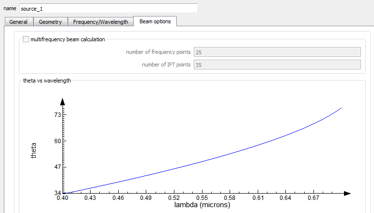
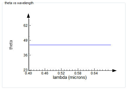
- THETA VS WAVELENGTH PLOT: This plot shows the actual injection angle theta for each source wavelength as used in the simulation.
Multifrequency beam calculation
- MULTIFREQUENCY BEAM CALCULATION checkbox enables/disables the calculation of the source profile at multiple frequency points. This feature is recommended for broadband simulations, and injection in a dispersive material, particularly if injection under an angle is involved. It is important to remember that if this option is not checked, the same spatial field profile at all frequencies is injected. See this dedicated topic for more information about this feature.
- NUMBER OF FREQUENCY POINTS specifies how many frequency points are going to be used to compute the field profile.
Beam options for Gaussian and Cauchy/Lorentzian sources
USE SCALAR APPROXIMATION / USE THIN LENS: These checkboxes allow the user to choose whether to use the scalar approximation for the electric field or the thin lens calculation. Gaussian sources can be defined using either the scalar approximation or thin lens calculation, whereas Cauchy/Lorentzian sources can only be defined using the scalar approximation.
VISUALIZE BEAM DATA: This button opens up a visualizer window where you can plot the current calculated beam electric and magnetic field profile over the injection plane.
Scalar approximation (Gaussian and Cauchy/Lorentzian)
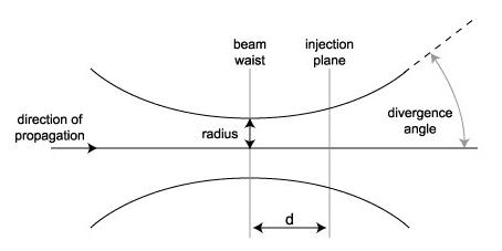
BEAM PARAMETERS: This menu is used to choose to define the scalar beam by the WAIST SIZE AND POSITION or the BEAM SIZE AND DIVERGENCE ANGLE.
If WAIST SIZE AND POSITION is chosen, the options are:
- WAIST RADIUS: 1/e field (1/e2 power) radius of the beam for a Gaussian beam, or a half-width half-maximum (HWHM) for the Cauchy/Lorentzian beam.
- DISTANCE FROM WAIST: The distance, d, as shown in the figure below. A positive distance corresponds to a diverging beam, and a negative sign corresponds to a converging beam.
If BEAM SIZE AND DIVERGENCE ANGLE is chosen, the options are:
- BEAM RADIUS: 1/e field (1/e2 power) radius of the beam for a Gaussian beam, or a half-width half-maximum (HWHM) for the Cauchy/Lorentzian beam.
- DIVERGENCE ANGLE: Angle of the radiation spread as measured in the far field, as shown in the figure below. A positive angle corresponds to a diverging beam and a negative angle corresponds to a converging beam.
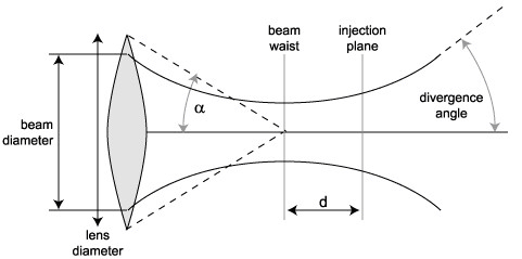
Thin Lens (Gaussian only)
- NA: This is n sin(a) where n is the refractive index of the medium in which the source is found and a is the half angle as shown in the figure below. Please note that the index will not be correctly defined in dispersive media and lenses should only be used in non-dispersive media. The refractive index for the source is determined at X, Y (and Z).
- DISTANCE FROM FOCUS: The distance d from focus as shown in the figure below. A negative distance indicates a converging beam and a positive distance indicates a diverging beam.
- FILL LENS: Checking this box indicates that the lens is illuminated with a plane wave which is clipped at the lens edge. If FILL LENS is unchecked, then it is possible to set the diameter of the thin lens (LENS DIAMETER) and the beam diameter prior to striking the lens (BEAM DIAMETER), as shown in the figure below. A beam diameter much larger than the lens diameter is equivalent to a filled lens.
- USE CUSTOM PUPIL FUNCTION: Checking this box applies a pupil (aperture) function to the beam. This option disables the FILL LENS one. The pupil function is defined in direction cosine space (i.e. normalized k-space) by a matrix dataset with parameters u1 and u2 on the plane perpendicular to the injection axis of the source. The matrix dataset must be called "pupil" and it must have either a single scalar attribute named "p" or two scalar attributes named "E1" and "E2"; the second case can be used to modify the polarization of the beam. The matrix dataset can be loaded from a matlab file using the LOAD PUPIL FUNCTION button or from the Lumerical script workspace using the command importdataset. For more information see this example.
- NUMBER OF PLANE WAVES: This is the number of plane waves used to construct the beam. The beam profile is more accurate as this number increases but the calculation takes longer. The default value in 2D is 1000.
| TIP: selecting the beam option When the beam waist radius is several times larger than the wavelength used, scalar approximation option should be selected. When the beam waist radius is roughly on the same order as the wavelength, the thin lens option should be used. |
| Note: References for the thin lens source The field profiles generated by the thin lens source are described in the following references. For uniform illumination (filled lens), the field distribution is precisely the same as in the papers. For non-uniform illumination at very high NA (numerical aperture), there are some subtle differences. This is due to a slightly different interpretation of whether the incident beam is a Gaussian in real space or in k-space. This difference is rarely of any practical importance because other factors such as the non-ideal lens properties become important at these very high NA systems. |
The figure below shows the beam parameter definitions for the scalar approximation beam.
The figure below shows the beam parameter definitions for the thin lens, fully-vectorial beam.
| TIP: Setting Gaussian source parameters Gaussian spot size: The beam spot size can be set independently of the source span. The source span should be chosen to be larger than the beam spot size. If the spot size is larger than the simulation region, the beam profile will be truncated at the simulation boundary. If there is significant intensity at the edges of the source, as shown in this figure, the beam will scatter on injection. | 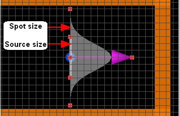 |
Results returned
- FIELDS: The fields injected at the injection plane is returned as a function of position and frequency/wavelength.
- INDEX: The index of the region the source covers is returned. This value does not refresh automatically, user needs to re-calculate the FIELDS.
- TIME SIGNAL: Time domain signal of the source pulse.
- SPECTRUM: The fourier transform of time signal.
Understanding field truncation issues with finite sized plane wave sources

This section describes problems that can occur when using the plane wave source is truncated, either because the span is too small, or when PML boundary conditions are used.
Examples of correct usage
Ideally the plane wave source should be used in the following manner: The source should span the entire simulation. Periodic or Bloch boundary conditions should be used in the directions normal to the propagation. PML should be used to to absorb the transmitted and reflected light.The first two examples illustrate this situation.
  | Description Simulate a plane wave propagating through free space at normal incidence. Simulation Settings
Results
Recommendations
|
  | Description Simulate a plane wave incident on a periodic array of cylinders at normal incidence. Simulation Settings
Results
Recommendations
|
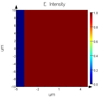
Truncation by PML boundaries
If PML boundary conditions are used in the direction normal to the wave-vector, some undesired diffraction will occur because of energy absorbed by the PML.
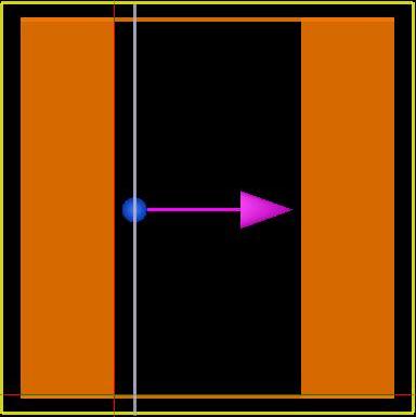
  | Description Simulate a plane wave propagating through free space, but with PML on all boundaries. Simulation Settings
Results
Recommendations
|
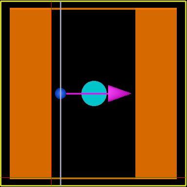
Truncation due to short source span
If the source does not span the entire simulation width, diffraction will occur at the source boundaries. Physically, this setup can be understood as an infinite plane wave passing through an aperture the size of the source. Diffraction occurs as the plane wave passes through the aperture.
  | Description Simulating a finite sized plane wave propagating in free space with the planewave source. Simulation Settings
Results
Recommendations
|
Understanding injection angles in broadband simulations
This page describes how to set up a simulation with a plane wave source injected at an angle. Issues that arise when using angled injection sources, including PML reflections, wavelength dependence of the injection angle, and other errors are also discussed. Even though only the plane wave source is discussed here, the same issues arise with all the sources including the mode source.
Note that the wavelength dependence issue can be avoided by using BFAST or multifrequency beam calculation for beam source and diffracting plane wave source.
Simulation setup
Source
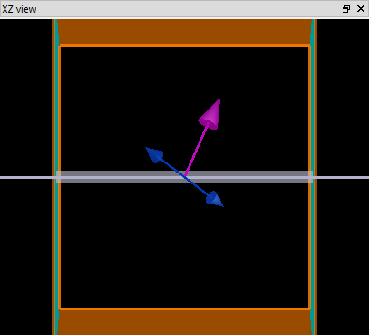
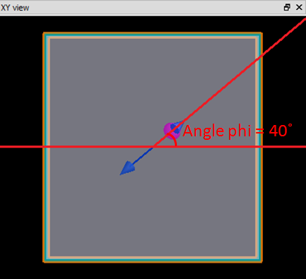
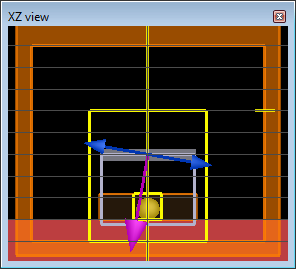
To set a non-zero injection angle for a plane wave source, edit the source object. In the GENERAL tab of the edit source window, set ANGLE THETA and/or ANGLE PHI (Angle Theta alone for 2D, both for 3D, if needed).
ANGLE THETA sets the angle with respect to the injection axis. In this example, the injection axis is the z-axis and the XZ view is shown below.
This angle of injection is then rotated around the injection axis by ANGLE PHI in a right-hand context. The XY view in the image below shows phi in our example.
Boundary conditions
Bloch boundary conditions are required when using a plane wave source injected at an angle. Bloch boundary conditions are similar to periodic boundary conditions, but they take into account a phase change across each period. Information about setting up Bloch boundary conditions can be found on the Bloch boundary conditions page.
However, when BFAST source technique is used, the boundary conditions set by the users in the plane of oblique incidence will be overridden by BFAST's own built_in boundary conditions.
PML reflections
When injecting at steep angles, light will strike the PML boundaries at grazing angles. PML boundaries are optimized to absorb light at normal incidence. At grazing angles of incidence, large PML reflections can decrease the accuracy of the simulation results. Increasing the number of PML layers will reduce reflections.
Steeper injection angles require more PML layers. In the multi-layer stack calculation example, the model setup script is used to set the minimum number of PML layers used based on the angle of injection of the source.
Broadband injection angles
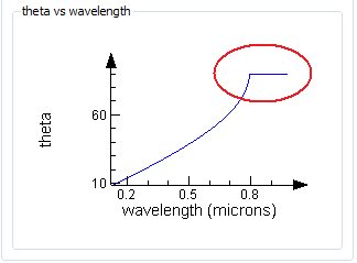
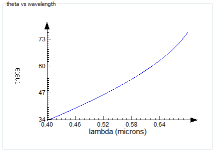
When a non-zero injection angle is set for Bloch/periodic plane wave source type, the actual angle of injected in the simulation varies as a function of frequency in broadband simulations. To get the actual angle injected at any particular wavelength, you can use the getsourceangle function, or edit the source to see a plot of theta versus wavelength in the GENERAL tab.
Background
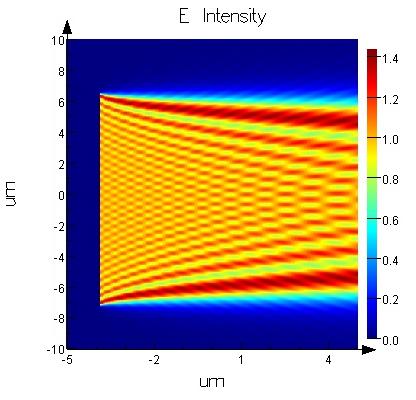
Bloch/periodic plane wave source injects fields that have a constant in-plane wavevector at all frequencies. The following figure shows a source with a nominal injection angle of approximately 45 degrees (purple arrow). The in plane wave vector (dotted green line) is chosen such that the actual injection angle at the center frequency fsim of the simulation matches the nominal injection angle. Since the magnitude of the wavevector is proportional to frequency, the actual injection angle will change as a function of frequency. Higher frequencies will be injected at smaller angles, while lower frequencies will be injected at larger angles.
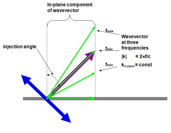
The in-plane wavevector is calculated with the following formula.
kin_plane=ksimsin(θsim)
where
ksim=2πfsimc
and θsim
is the nominal injection angle, fsim is the center frequency of the source, n is the refractive index and c
is the speed of light.
Since the magnitude of the wavevector is a function of frequency, while the in-plane component is fixed, the injection angle must change as a function of frequency. The angular dependence can be calculated with the following formula:
sin[θ(f)]=kin−planek(f)=sin(θsim)fsimf
θ(f)=arcsin[sin(θsim)fsimf]
Therefore, while broadband sources can inject at angles, it must be recognized that the injection angle will change as a function of frequency. At close to normal incidence, the change in angles is smaller than at steeper angles. A source injecting light at 450 to 550 nm with a 5 degrees nominal incidence angle will actually inject at angles between 4.5 and 5.5 degrees. If the nominal angle is increased to 25 degrees, the range of angles will be between 23 and 28 degrees.
The getsourceangle function can be used to get the actual injection angle as a function of frequency. This data is also displayed in the GENERAL tab of the Plane wave and Gaussian sources.
Injection angle example
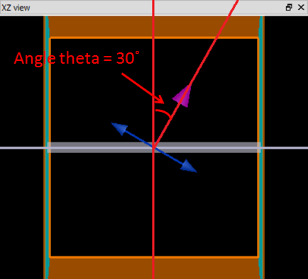
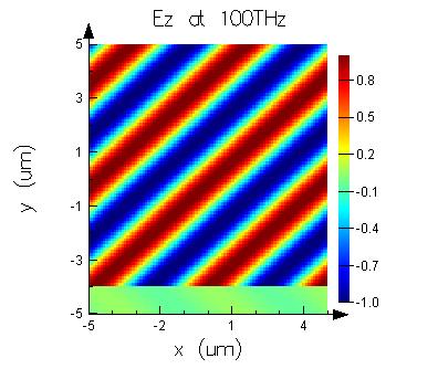
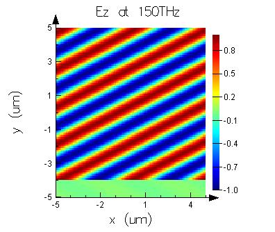
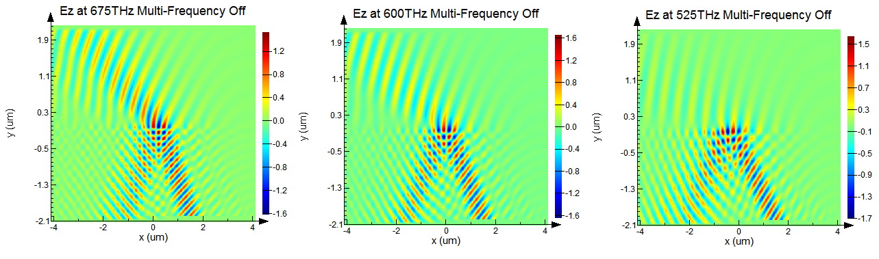
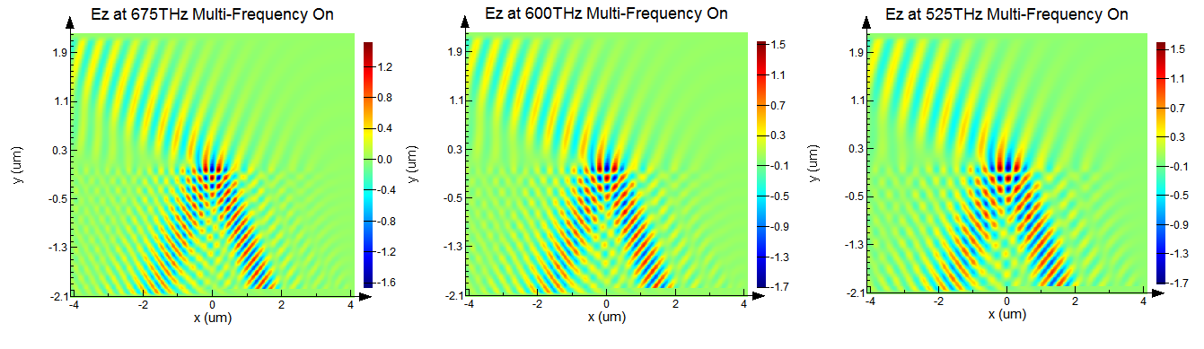
In usr_broadband_injection_angles.fsp, the source injection angle is 30 degrees, and the frequency range is 100 to 150 THz (2-3um).
Run the simulation, then run associated script. The script first calculates the actual injection angle vs frequency with the getsourceangle function.
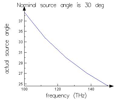
Notice that the injection angle changes as a function of frequency. At low frequencies, the injection angle is almost 40 degrees. At high frequencies, the angle is about 25 degrees.
Next, the script plots the fields profile at 100 and 150 THz. Both figures are from the SAME simulation. The actual propagation direction is obviously different.
|
Field profile at 100THz. Angle is about 40 degrees. |
Field profile at 150THz. Angle is about 25 degrees. |
| Note: What to do If you encounter broadband injection angle error in your simulation, there are two options you can choose from to avoid this problem: you can run a series of narrowband simulations or run a series of single frequency simulations. When using a series of narrowband simulations, you need to again check to make sure that the angle deviance is at an acceptable level. If not, you would have to use a series of single frequency simulations to obtain accurate results. When running these series of simulations, a feature that is very helpful is the parameter sweep. BFAST can avoid this problem due to its special formulation, please refer BFAST page. |
| Note: Bloch vector with Bloch boundary conditions When using bloch boundary conditions, the bloch vector should be set to kSIM. The Bloch BC option "set based on source angle" automatically sets the correct Bloch vector. |
| Note: Angle going past 90 degrees When the center angle is going past 90 degrees, the source in an attempt to inject angle above 90 degrees injects evanescent fields. And this behavior is not desirable, and simply state, the source is not able to inject above 90 degrees. When the center angle is large and/or when the source is more broadband, this issue is more likely to occur. In such situations, it is usually necessary to reduce the center angle or source wavelength range.
|
In order to get broadband results at a certain source angle, a parameter sweep task can be set up to run a series of single frequency simulations sweeping over the frequency range of interest. A guide to setting up parameter sweeps is available at the Parameter sweep tasks page.
To get the broadband results over a range of injection angles, a nested sweep can be set up to sweep over the range of injection angles and source frequencies. The Nested sweeps page provides a tutorial.
Additionally, this issue can be avoided by using BFAST instead of Bloch/periodic plane wave source.
Injection errors
In broadband simulations with angled injection sources, there can be large injection errors at frequencies outside of the center frequency. This can lead to errors if you use the transmission through a monitor placed behind the source to measure reflected power. The alternative technique of using a monitor placed in front of the source is described on the Measuring reflection page.
Advanced
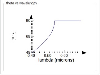
Longer source pulse
A longer source pulse can be used in the case where you are running a broadband simulation and injecting at a steep angles where wavelengths beyond a certain threshold are injected at 90 degrees. In the following image you can see that for this particular source setup, the wavelengths above approximately 0.8um will be injected at 90 degrees.
When light is injected at 90 degrees, it propagates across the simulation interfering constructively with itself. At these wavelengths, there can be a large field intensity because the light does not propagate out of the simulation region. The Fourier transform of the time signal will have a large peak corresponding to the wavelengths injected at 90 degrees, and the sidelobes of this peak can create noise at wavelengths of interest.
By default, FDTD uses the shortest possible source pulses in the time domain, which means they have a much broader spectral content than the specified source wavelength range. A longer source pulse will have narrower spectral content, and it is possible to increase the length of the source pulse until spectrum of the source pulse does not include the wavelengths that are injected at 90 degrees.
 The spectrum vs wavelength is plot for the default source pulse. A significant amount of power is injected at wavelengths above 0.8um. |
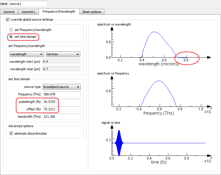 The spectrum for a source pulse where the pulselength and offset have been increased to 10 times the default values. The power at wavelengths above 0.8um are reduced. |
Interpolation
Another method for getting broadband results over a range of injection angles is discussed in Bloch BCs in broadband sweeps over angle of incidence. This method uses broadband simulations and runs one parameter sweep over a range of injection angles. This requires fewer simulations than the nested sweep method, but involves more post-processing to interpolate the data to a common source angle vector.
Since BFAST source fixes the incident angle for all the frequencies set in the source, the above interpolation is not necessary, as one simulation can give broadband results at the given angle. When users want to get broadband results at many different incident angles, a sweep of incident angles can be used. No interpolation will be needed since the sweep can give broadband results as a function of incident angles.
Understanding the diffracting option of the plane wave source
The purpose of this section is to describe how diffracting plane wave source works and how it differs from Bloch/periodic plane wave source. Well know double slit experiment is used to demonstrate this.
Discussion and simulation setup
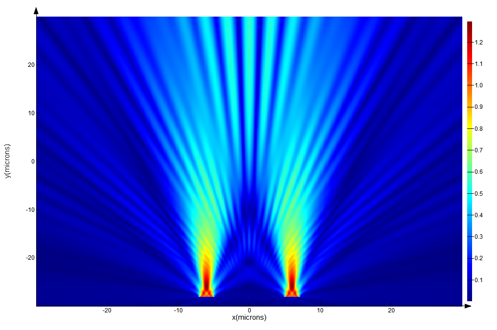
| Diffracting plane wave source is a source in which plane wave propagates through a rectangular aperture. The size of the source defined on the Geometry tab is the dimension of the aperture. Additionally, diffraction pattern will be produced as the plane wave travels through the aperture. This differs from the Bloch/periodic plane wave source type, which always automatically expands across the size of the entire simulation region in order to simulate pure plane wave. For this reason, diffracting plane wave source should be used only in simulations where the diffraction is a desirable effect. In case of the double slit experiment, the diffracting plane wave source allows us to replace each slit with a plane wave source instead of creating a structure representing the slits. In this example, the sources are 12um apart and each source/slit has size of 2um. Frequency domain field and power monitor is used to represent the screen that is placed 58um from the slits. | 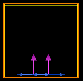 |
The following analytical formula can be used to calculate the spacing of the interference maxima on the projection plane:
s=zλd
where:
z is the distance of the projection plane from the slits
d is the distance between the slits
lambda is wavelength
Simple calculation shows that the distance between the maxima at 633nm should be approximately 3.05um.
| Tip: Reducing the simulation size To minimize the simulation time, it is generally recommended that you do not include large regions of empty space in a simulation. It would be possible to obtain these same results with a much smaller simulation region, by taking advantage of the far field projection functions. This example uses a large simulation region to keep the analysis as simple as possible, even though it is less computationally efficient. |
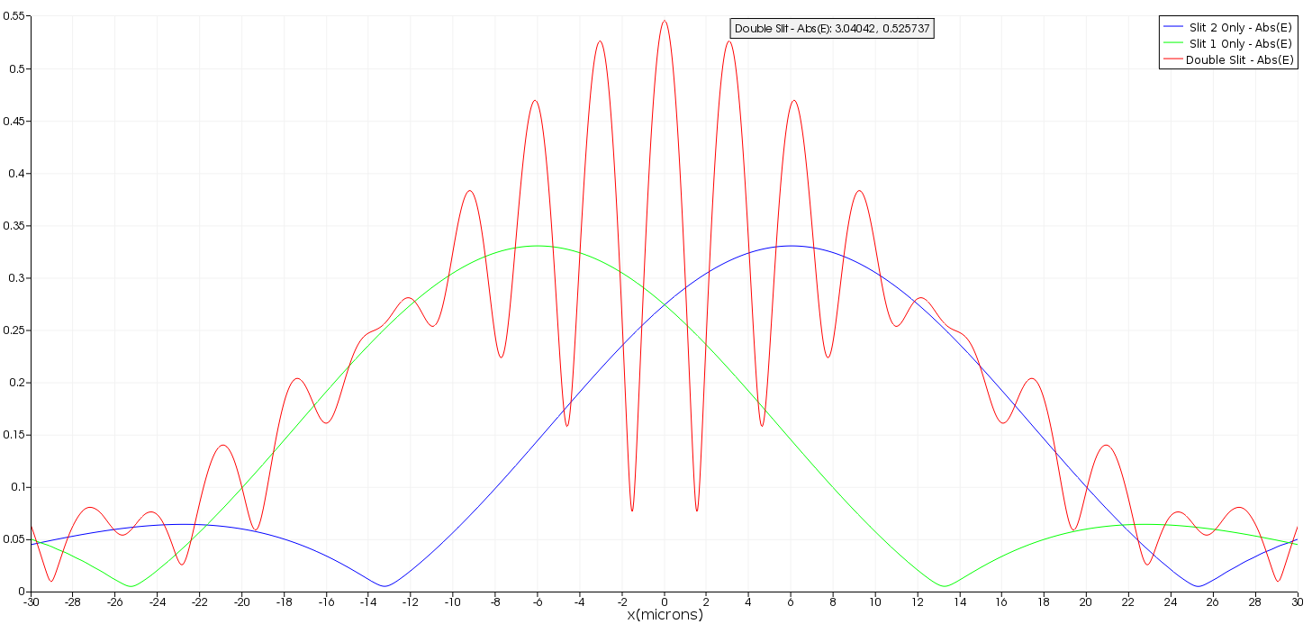
Results
The simulation results shown on the figures below demonstrate the diffracting nature of the sources and their constructive and destructive interference. Moreover, the distance between the maxima is ~3.04um, which is well aligned with the analytical result above.
 |  |
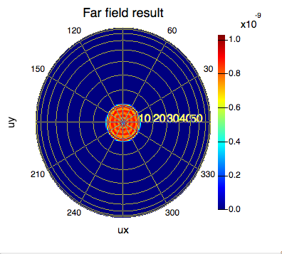
Defining a beam using a pupil function
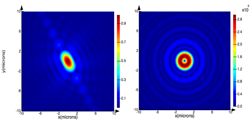
In this article, we describe two examples of how to use the pupil (aperture) function option available in the Gaussian beam source. In the first example, we define a half-circle aperture using a scalar pupil function while in the second one we create beams with radial and azimuthal polarizations using a vectorial pupil function.
Simulation setup
The associated files script files show how to construct and apply a pupil (aperture) function to a Gaussian beam source with the thin lens option:
- The pupil function is defined in direction cosine space by constructing a mesh grid for ux and uy within the maximum beam numerical aperture (NA). Note that it is not necessary to cover the entire k-space up to NA=1, as the maximum NA used will be the maximum NA where the pupil function is not zero.
- The scripts import the matrix datasets with the pupil function directly in the Gaussian beam source. These datasets are also saved in MATLAB files that can be imported into the source using the "load pupil function" button in the "Beam options" tab of the source settings.
Results
Open pupil_function_beam.fsp and run the script files. After setting up and applying the pupil function, the associated scripts will run the simulations and plot the fields recorded by a monitor in front of the source. The normalized reflected power measured by a monitor behind the source is of the order of 1e-6, indicating that there are very small injection errors.
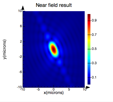
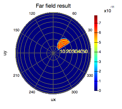
Near-field and far-field fields for x-polarized beam with a half-circle aperture, incident at theta and phi angles of 20 and 30 degrees, respectively.
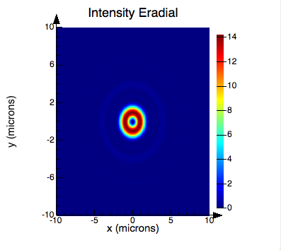
Near-field and far-field fields for radially-polarized beam with circular aperture at normal incidence. Only the radial component of the near field is shown here; as expected, the azimuthal component is negligible.
| Note:
|
Understanding frequency dependent profiles for sources in FDTD (advanced)
Please note that this is an advanced source feature that can substantially increase simulation time, and we don’t recommend using it unless strictly necessary. If you choose to use the frequency dependent profile option, we strongly recommend beginning all simulations without this feature, and only proceeding to using it after all other project settings have been configured and you are obtaining good results at the center frequency of your simulation.
Requirements
Control of the maximum convolution time window requires 2020a R4 or newer.
Default injection method
FDTD sources that are injected on a plane (gaussian, plane, custom, mode and ports) are injected into the FDTD simulation using electric and magnetic fields as a function of time that are given by:
→EFDTD(x,y,z0,t)=→Esource(x,y,z0,ω0)s(t)
→HFDTD(x,y,z0,t)=→Hsource(x,y,z0,ω0)s(t)
where ω0=2πf0
is the angular frequency corresponding to the center frequency of the FDTD simulation, →Esource(x,y,z0,ω0) and →Hsource(x,y,z0,ω0) are the frequency domain electric and magnetic source profiles calculated at the center frequency of the simulation, and s(t) is the source time signal∗
.
∗
Note that s(t) is calculated for all sources based on the input parameters in the “Frequency/Wavelength” tab. In most cases, the user simply chooses a target wavelength range and the optimal source signal s(t) is automatically calculated. Less frequently, the user will adjust the time domain parameters or define a custom time signal for s(t). Frequency domain data is normalized to the frequency spectrum of the source signal, s(ω)
, to obtain the impulse response of the system; see Understanding frequency domain CW normalization for more details.
When to use frequency dependent profiles
For many simulations, the default approach is appropriate since the source profile has a negligible variation over the bandwidth of the simulation. However, there are some cases where frequency dependent profiles should be used:
- Beam sources (gaussian or thin lens) where the source profile changes substantially over the simulation bandwidth. The beam profile becomes increasingly frequency dependent as the beam NA increases.
- Mode sources or ports where the mode profile changes substantially over the bandwidth.
- Beam sources at angles where a frequency independent source angle is desired. The frequency dependence of the angle of injection increases with increasing nominal source angle.
- Plane waves injected at angles where a frequency independent source angle is desired. Note that this will be a diffracting plane wave, so consider BFAST as an alternative for periodic structures.
- Plane waves injected into a dispersive medium where the ratio of →E
and →H
- changes substantially with frequency.
When NOT to use frequency dependent profiles
If you are working with linear materials and have a source profile that can be written as the product of functions of space and frequency as
→Esource(x,y,z0,ω)=→Espatial(x,y,z0)g(ω)
→Hsource(x,y,z0,ω)=→Hspatial(x,y,z0)g(ω)
then you should NOT use frequency dependent profiles, no matter how complex the frequency dependence of g(ω)
. To improve performance, multiply the →E and →H fields collected by frequency domain monitors by g(ω)
as a post-processing step following the FDTD simulation. This works because the standard usage of FDTD (with cw normalization on) calculates the impulse response of the system.
How they work
When using frequency dependent source profiles, the electric and magnetic fields injected into the FDTD simulation are given by
→EFDTD(x,y,z0,t)=FT−1{→Esource(x,y,z0,ω)s(ω)}=→Esource(x,y,z0,t)∗s(t)
→HFDTD(x,y,z0,t)=FT−1{→Hsource(x,y,z0,ω)s(ω)}=→Hsource(x,y,z0,t)∗s(t)
Where FT−1
is the inverse Fourier transform. In the time domain, we therefore have a convolution product of the source pulse and the time domain source field profile.
In order to calculate the convolution product, we must be able to accurately interpolate the source profile in the frequency domain. Since many beam calculations are computationally expensive, especially thin-lens and mode sources, we use Chebyshev interpolation and therefore sample the profile on a Chebyshev frequency grid. This provides the optimal discrete sampling grid to approximate the continuous functions →Esource(x,y,z0,ω)
and →Hsource(x,y,z0,ω)
.
The convolution product results in injected fields (→EFDTD(x,y,z0,t)
and →HFDTD(x,y,z0,t)
) the duration of which cannot be known beforehand; it depends on the complexity of the frequency dependence of the source field. FDTD will attempt to autodetect the injected pulse duration and may allow the injected pulse to last for the entire FDTD simulation. In addition, when sources are injected at angles, additional time may be added to the FDTD simulation because the injected pulse will arrive at different times across the source plane. Longer simulations, and longer times required to inject the beam are the main computational costs associated with injecting frequency dependent beam profiles.
Meaning of the settings
- number of field profile samples is the number of frequency samples of the source profile we take on a Chebyshev grid for the subsequent calculations. The number of points required depends greatly on how much frequency dependence the profile has with frequency. We recommend starting with a small number (such as 7) and increasing it using usual convergence testing approaches.
- set maximum convolution time window and maximum convolution time window allow you to optionally limit the maximum amount of time that will be used for the injected pulse generated by the convolution product. When unchecked, the maximum convolution time window is equal to the maximum simulation time.
Custom field profiles
When you load custom source field profiles they will be used to create →Esource(x,y,z0,ω)
and →Hsource(x,y,z0,ω)
. If you load only a single frequency, there is no purpose in turning on frequency dependent profiles. If you load multiple frequencies, the data will be interpolated onto the Chebyshev grid that covers the specified frequency range of the source, using the number of field profile samples specified. There are no restrictions on the frequency sampling of your custom data, or even that there is perfect overlap between the frequency range of the data and the frequency range of the source. However, for greatest accuracy with the least amount of custom data, it is best to load custom data sampled on a Chebyshev grid that corresponds to the same frequency range you intend to use for your source, and choose the number of field profiles samples to be equal to the number of frequency samples in your data. If the field data comes from a prior FDTD simulation, you can easily choose to sample frequency domain monitors on a Chebyshev grid.
Frequency extrapolation
In order to calculate the convolution product, the field profile data must be extrapolated outside the frequency range provided to all frequencies that may be present in the FDTD simulation. The choice of extrapolation method does not affect the final FDTD results calculated within the desired simulation bandwidth, but it can affect the length of the convolution time window required for the simulation. By default, we use a fourth order polynomial extrapolation that preserves the continuity of the first and second derivatives at the edge of the simulation bandwidth. Since release 2020 R2.2, we allow advanced users to control the extrapolation method used for imported field profiles and mode sources by allowing a third order extrapolation that preserves only the continuity of the first derivative at the edge of the simulation bandwidth. This can be necessary because an incorrect second derivative may lead to significant overshoot effects when extrapolating using the fourth order scheme. This advanced property, called "frequency extrapolation" is accessible only through script and has the following options:
- "auto" is the default value. With this setting, fourth order extrapolation will be used if the frequency grid is a Chebyshev grid and, otherwise, third order will be used because the interpolation step loses the accuracy of the second derivative.
- "fourth order" and "third order" can be used to force either extrapolation method. Third order may be desirable if, despite having a Chebyshev grid, there are any errors in the data that affect the accuracy of the second derivative.
The property can be written and read with the script commands set, get, setnamed and getnamed. For example,
set("frequency extrapolation","third order");
can be used when an imported source or mode source is selected.
Performance considerations
Increasing the number of field profile samples can greatly increase the initialization time, particularly for large, thin-lens sources. For mode sources and ports, it can increase the time to save files because the modes are pre-calculated in the design environment.
The convolution product itself is computationally expensive during the FDTD simulation and you may see the simulation speed slow substantially while the source is injected. The maximum duration of the injected pulse is stored as a result for the source called “convolution_time_window”. In 2D the result name has “_TE” or “_TM” appended because sources can create both TE and TM simulations, depending on the source polarization, and each type of source may have a different convolution time window. You may choose to limit the maximum convolution time window for two reasons:
- You are running a simulation with a very long maximum simulation time that is substantially longer than the convolution time window required. Limiting the maximum convolution time window over which the source will attempt to determine the actual necessary convolution time window will improve the performance of the source during initialization.
- You decide that the convolution time window determined by the source is longer than necessary and includes a long period of very weak source signal, which can be ignored. If you reduce the maximum convolution time window for this reason, it will likely reduce the accuracy of the results, but it may be an acceptable tradeoff. Also, this will improve performance while the simulation is running because it is reducing the amount of time the source is actually injected, and may even reduce the total simulation time by allowing the autoshutoff conditions to occur sooner.
In either case, if you reduce the maximum convolution time window it is worth monitoring the result “convolution_time_window” to be sure you understand which of the above situations you are in, and what the impact on performance and accuracy may be.
Advanced method to improve performance
You should use frequency dependent source profiles if you are working with linear systems and can write the field profile as
→Esource(x,y,z0,ω)=→Esimple(x,y,z0,ω)g(ω)
→Hsource(x,y,z0,ω)=→Hsimple(x,y,z0,ω)g(ω)
where g(ω)
has complicated frequency dependence and the frequency dependence of →Esimple(x,y,z0,ω) and →Hsimple(x,y,z0,ω) has very little frequency dependence (in amplitude and phase) but enough that it cannot be ignored entirely. In this case, use →Esimple(x,y,z0,ω) and →Hsimple(x,y,z0,ω) as the frequency dependent source profile. Then, AFTER the FDTD simulation, multiply the →E and →H fields collected by frequency domain monitors by g(ω)
. This can greatly reduce the duration of the convolution time window as well as the total simulation time until the autoshutoff conditions are met, while giving the same results.
Examples
Frequency dependent beam profile example
As discussed above, when the frequency dependent profile calculation is disabled, the beam profile is calculated only for the center frequency. Enabling this option then makes the beam profile frequency dependent and allows for more physically accurate broadband simulation. The images below demonstrates how much the beam profile changes with wavelength from 400nm to 1000nm for a filled thin lens beam with NA=0.6:
Broadband injection angles example
As discussed above, another type of simulation that can greatly benefit from the frequency dependent profiles are broadband simulations with angled injection of beams. The figure below shows a comparison of a beam that is injected at a nominal angle theta=45 degrees over a range of wavelengths from 400nm to 700nm. With frequency dependent beam profiles, the source injects light under a constant angle of 45 degrees, however, when the feature is disabled the injection angle ranges from 34 degrees at 400nm to almost 80 degrees at 700nm.
The following example is using a 2D field monitor to demonstrate the propagation of a Gaussian beam injected at an angle and interacting with a dielectric/air interface. The plots below show how the frequency dependent profile calculation can benefit the reflection/transmission simulations since the R/T characteristics are highly dependent on the angle of incidence. See the associated files to run this example on your computer. This example also demonstrates that the frequency dependent profile calculation has negligible simulation time penalty in 2D mode despite the fact that the number of field profile samples is set to 125. In 3D such a large number of field profile samples can have a more significant computational cost.
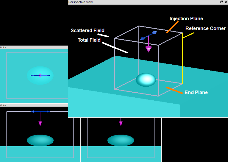
Total-Field Scattered-Field (TFSF) source - Simulation object
 The TFSF source is often used to study scattering from small particles illuminated by a plane wave. Typical uses include:
- Particles in a homogeneous medium (which may be lossy or anisotropic). E.g. Mie scattering
- Non-periodic structures in a multi-layer substrate, which may be lossy or anisotropic.
- Periodic structures in a multi-layer substrate, when used in conjunction with Periodic or Bloch boundary conditions.
The TFSF source separates the computation region into two distinct regions:
- Total Field region - includes the sum of the incident field wave plus the scattered field
- Scattered Field region - includes only the scattered field.
The TFSF source is an advanced source and care must be taken to ensure proper setup and analysis of results. See TFSF tips and best practices for more information. Both regions are visible in the top figure. It is important to note that the physical field is the total field and the separation into an incident and a scattered field requires careful interpretation. For particles in a homogeneous medium, the incident field is a plane wave. For particles on a substrate or multi-layer stack, the incident field is the field that would exist in the multi-layer in the absence of a particle (or defect).
| NOTE: The following changes have been made to the polarization arrows in 2020 R.1.4 to avoid ambiguity with the polarization orientation.
These changes affect only the way the source objects look in the GUI. The simulation results won't be affected in any way. |
General tab
- INJECTION AXIS: Sets the axis along which the radiation propagates.
- DIRECTION: This field specifies the direction in which the radiation propagates. FORWARD corresponds to propagation in a positive direction, while BACKWARD corresponds to propagation in a negative direction.
- AMPLITUDE: The amplitude of the source as explained in the Units and normalization section.
- PHASE: The phase of the point source, measured in units of degrees. Only useful for setting relative phase delays between multiple radiation sources.
- ANGLE THETA: In 3D simulations, this is the angle of propagation, in degrees, with respect to the injection axis of the source. In 2D simulations, it is the angle of propagation, in degrees, rotated about the global Z-axis in a right-hand context, i.e. the angle of propagation in the XY plane.
- ANGLE PHI: In 3D simulations, this is the angle of propagation, in degrees, rotated about the injection axis of the source in a right-hand context. In 2D simulations, this value is not used.
- POLARIZATION ANGLE: The polarization angle defines the orientation of the injected electric field, and is measured with respect to the plane formed by the direction of propagation and the normal to the injection plane. A polarization angle of zero degrees defines P-polarized radiation, regardless of the direction of propagation while a polarization angle of 90 degrees defines S-polarized radiation.
- THETA VS WAVELENGTH PLOT: This plot shows the actual injection angle theta for each source wavelength as used in the simulation.
Geometry tab
The geometry tab contains options to change the size and location of the sources.
Frequency/Wavelength tab
The Frequency/Wavelength tab is shown below. This tab can be accessed through the individual source properties, or the global source properties. Note that the plots on the right-hand side of the window update as the parameters are updated, so that you can easily observe the wavelength (top figure), frequency (middle figure) and temporal (bottom figure) content of the source settings.

At the top-left of the tab, it is possible to chose to either SET FREQUENCY / WAVELENGTH or SET TIME-DOMAIN. In most simulations, the 'SET FREQUENCY / WAVELENGTH ' option is recommended.
f you choose to directly modify the time domain settings, please keep the following points in mind:
- PULSE DURATION: Choose a pulse duration that can accurately span your frequency or wavelength range of interest. However, very short pulses contain many frequency components and therefore disperse quickly. As a result, short pulses require more points per wavelength for accurate simulation.
- PULSE OFFSET: This parameter defines the temporal separation between the start of the simulation and the center of the input pulse. To ensure that the input pulse is not truncated, the pulse offset should be at least 2 times the pulse duration. This will ensure that the frequency distribution around the center frequency of the source is close to symmetrical, and the initial fields are close to zero at the beginning of the simulation.
- SOURCE TYPE: In general, you can choose between ‘standard’ and ‘broadband’ source types. Standard sources consist of a Gaussian pulse at a fixed optical carrier, while the broadband sources consist of a Gaussian pulse with an optical carrier which varies across the pulse envelope. Broadband sources can be used to perform simulations in which wideband frequency data is required – for instance, from 200 to 1000 THz. This type of frequency range cannot be accurately simulated using the standard source type.
Set frequency wavelength
If the SET FREQUENCY / WAVELENGTH option was chosen, this section makes it possible to either set the frequency or the wavelength and choose to either set the center and span or the minimum and maximum frequencies of the source.
For single frequency simulations, simply set both the min and max wavelengths to the same value.
Set time domain
The options in the time domain section are:
- SOURCE TYPE: This setting is used to specify whether the source is a standard source or a broadband source. The standard source consists of an optical carrier with a fixed frequency and a Gaussian envelope. The broadband source, which contains a much wider spectrum, consists of a chirped optical carrier with a Gaussian envelope. When the user uses the script function setsourcesignal, this field will be set as "user input".
- FREQUENCY: The center frequency of the optical carrier.
- PULSELENGTH: The full-width at half-maximum (FWHM) power temporal duration of the pulse.
- OFFSET: The time at which the source reaches its peak amplitude, measured relative to the start of the simulation. An offset of N seconds corresponds to a source which reaches its peak amplitude N seconds after the start of the simulation.
- BANDWIDTH: The FWHM frequency width of the time-domain pulse.
For more information, please visit Changing the source bandwidth
Advanced
- ELIMINATE DISCONTINUITY: Ensures the function has a continuous derivative (smooth transitions from/to zero) at the start and end of a user-defined source time signal. Enabled by default.
- OPTIMIZE FOR SHORT PULSE: Use the shortest possible source pulse.
- This option is enabled by default in the FDTD solver. It should only be disabled when it is necessary to minimize the power injected by the source that is outside of the source range (eg. convergence problems related to broadband steep angled injection).
- This option is disabled by default in the varFDTD solver, as it improves the algorithms numerical stability.
- ELIMINATE DC: Eliminates the DC component by forcing signal symmetry
Manual calculation of the source time signal
As explained above, the 'Standard' source type uses a fixed carrier with a Gaussian envelope. The following script code shows how to calculate the source time signal used by the source.
# calculate standard pulse time signal
frequency  = 300e12;
pulselength = 50e-15;
offset   = 150e-15;

t      = linspace(0,600e-15, 10000);
w_center  = frequency*2*pi;
delta_t   = pulselength/(2*sqrt(log(2)));
pulse = sin( -w_center*(t-offset)) * exp( -(t-offset)^2/2/delta_t^2 );

plot(t*1e12,pulse,"t (fs)","source pulse time signal");
| Note: There are some small differences between the pulse generated by this code and the actual time signal generated by the 'standard' source pulse setting. If you need very precise control over or knowledge of the source time signal, you should create your own Custom time signal. The 'broadband' option is generated with a more complex function. The precise function is not provided. To create your own arbitrary source time signals, see the Custom time signal page. |
Results returned
- TIME SIGNAL: Time-domain signal of the source pulse.
- SPECTRUM: The Fourier transform of the time signal.
Tips and best practices when using the FDTD TFSF source
The page provides further information on the correct usage of the TFSF source.
Understanding the TFSF source
The TFSF source is an advanced version of the plane-wave source designed primarily for particle scattering simulations, where the particle may be in a homogeneous medium or on a multi-layer substrate. When adding a TFSF source to a simulation, the most visible difference between the TFSF source and all other sources is that it appears as a 3D box, rather than a 2D plane. As shown in the above figure, one side of the source will be the Injection plane. The source will inject a plane wave from this side of the source. This aspect of the source is very similar to all other sources.
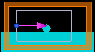
The slightly confusing aspect is that the source will then 'subtract' the same plane wave when it arrives at one of the boundaries of the source. This is much easier to understand with an example. The following screenshots show the behavior of the TFSF source in free space. Notice that the fields are injected at one edge, and are then 'subtracted' at the other edge. Also notice that the fields are zero in the 'Scattered field' region, since there are no scattering objects inside the source. The subtraction happens at the boundaries of the source and a reference 1D line at the top right corner of the TFSF boundary is used to determine the index profile of all the boundaries. For this reason, it is important to make sure the Reference corner (yellow line in the above figure), always goes through the substrate and NOT the feature for which we want to calculate scattering.
Simple example of TFSF with empty space
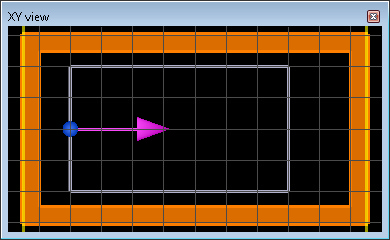
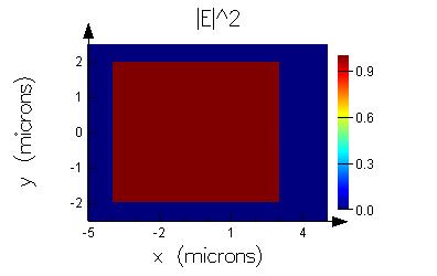
Simulating empty space is always a good starting point. The second figure shows a movie of Ez(t). The plane wave was injected along the left edge and propagates in the positive X direction. The third figure shows results from a frequency monitor of the CW fields. An intensity of 1 is measured within the TFSF source, while 0 is measured outside. There were no structures to cause any scattering, so the field remained an ideal plane wave inside, with an amplitude of 1. Similarly, the fields are zero in the scattered field region since there were no scattering objects in the simulation.
Important settings
Orientation of the source with respect to the structure
When adding a TFSF source to your simulation, ensure the following conditions are satisfied:
- The scatterer must be completely inside the TFSF source. The boundaries of the source cannot extend through the scattering object.
- The injection axis of the source must be normal to the substrate. In other words, all sides of the TFSF source must 'see' the same refractive index profile along the direction of propagation. The following figures show one example of a valid setup and one example of an invalid setup.

VALID: The injection axis is normal to the Gold and Glass layers. Also, each side of the source 'sees' the same refractive index profile (Air - Gold - Glass) along the direction of propagation, from the Injection plane to the End plane.
NOT VALID: The injection axis is not normal to the substrate. Also, the upper side of the source 'sees' a refractive index of air, while the lower side 'sees' the substrate index.
Extending through simulation boundaries
In most cases, the TFSF source should not be extended through the simulation boundaries. The only exception is that the TFSF can be extended through Periodic or Bloch boundaries.
INVALID: Extending source through PML boundaries
NOT VALID: Extending source through PML boundaries
VALID: Extending source through Periodic boundaries
Non-uniform mesh
The TFSF supports the use of non-uniform mesh within the source. However, for best results, the mesh should be uniform in the directions normal to the direction of propagation. For example, if the source is injecting along the z-axis, the x,y mesh should be uniform within the TFSF source. This detail is particularly important when the source angle is non-zero. See the "Particle on a surface at non-normal incidence" section below for more information.
Non-normal angles of incidence
When using non-normal angles of incidence, please take the following precautions
- Remember that the angle of incidence is still wavelength-dependent, as with other beam and plane wave sources. Please see Plane waves - Angled injection for more details.
- For best results, you should use a mesh override region over the entire x, y, and z span of the source so that the mesh is uniform over the source.
- For normalization, please note that the sourceintensity is defined with respect to the principle injection plane of the source. There may be a factor of cos(theta) that needs to be applied to your result. Please see the section Cross sections and normalization.
Tips for testing your setup
The best way to test your setup is to temporarily disable the particle or defect, run your simulation, and perform your subsequent analysis. This will allow you to determine the noise floor and immediately see if something is wrong with your setup. For example, if you are measuring the scattering and absorption cross-section of a particle on a surface, you should expect to find a scattering and absorption cross-sections of 0. In most cases, your defect or particle will have a mesh override region so that the mesh will not change when the defect is disabled. Typically the magnitude of the electric field in the scattered field region without a defect should be approximately 1e-7 when the incidence field amplitude is on the order of 1.
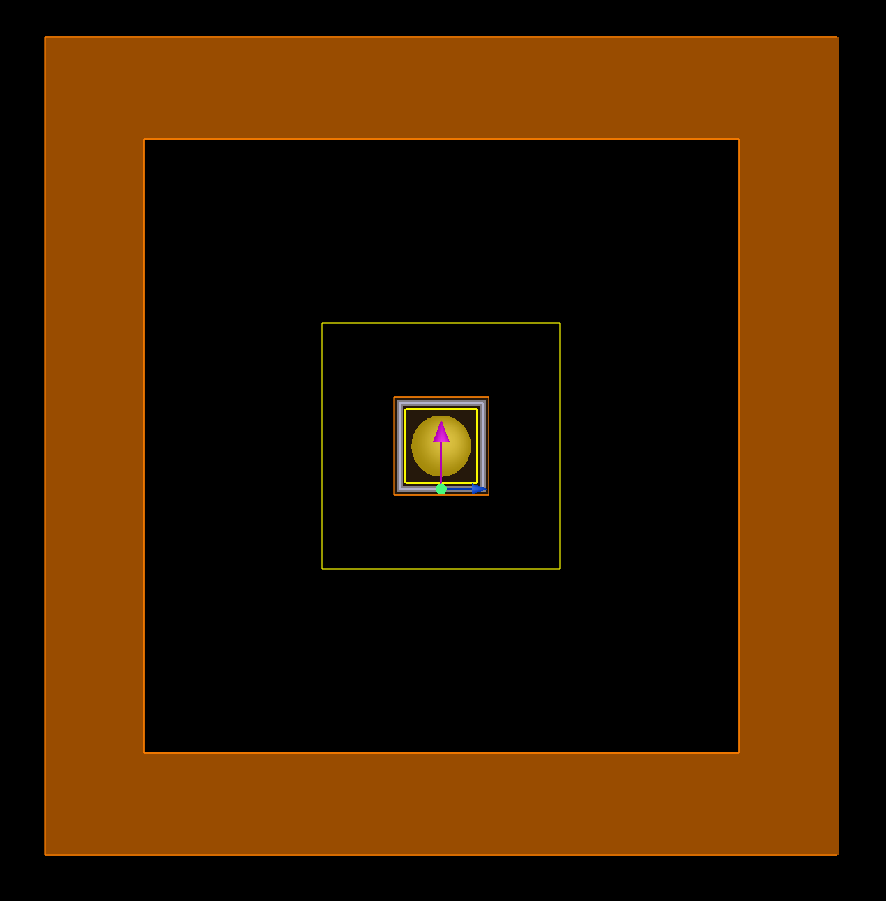
The simulation setup with a TFSF source at a non-normal angle of incidence.
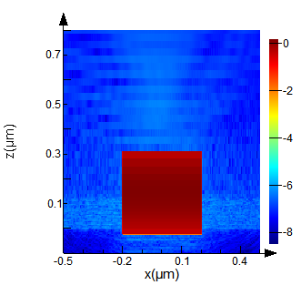
The magnitude of the electric field with the particle disabled on a log scale. Note that the field in the scattered field region is on the order of 1e-7, while the field in the total field region is on the order of 1.
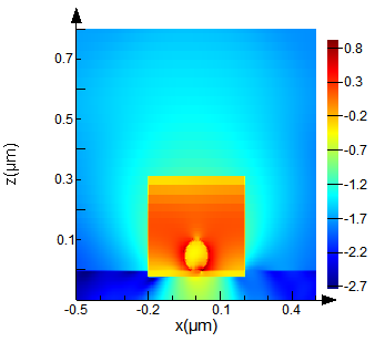
The magnitude of the electric field with the particle enabled on a log scale. We now have confidence that the scattered field (on the order of 1e-3 to 1e-1) is correct and well above the noise floor.
Power normalization
Power normalization with the TFSF source can be slightly confusing, particularly when the data is normalized by the power injected by the source.
This issue is best illustrated with an example. The following screenshots show a Mie scattering simulation, where a small gold sphere is illuminated by a plane-wave using the TFSF source.
The goal of the simulation is to measure the amount of power absorbed by the particle when it is illuminated by a plane wave. After running the attached simulation file (mie_scattering_fdtd.fsp), run the script ( mie_scattering_power_norm.lsf) to reproduce the following results based on different ways of calculating and normalizing the absorbed power.
Power in Watts
One option is to calculate the absorption in units of Watts. In this particular simulation, we can see that the particle absorbs about 2.7e-17 W of power at 530nm (for a plane-wave with an amplitude of 1V/m).
When the data is presented in this form (i.e. power in Watts), it is straightforward to understand and interpret.
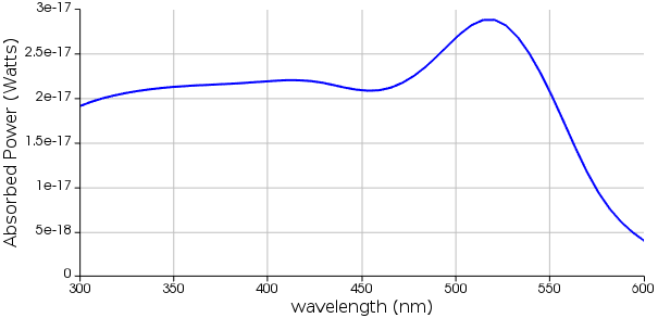
Power normalized to the source power
Alternatively, the data can be normalized to the power injected by the source.
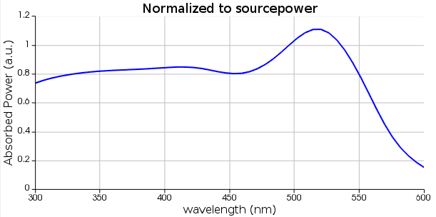
This type of normalization is quite common. For example, the 'transmission' script function automatically normalizes the power transmission data to the source power. While this normalization is often very convenient, it is not well suited to simulations using the TFSF source. The fundamental problem is that an ideal plane wave has infinite power (since it has an infinite extent), while a single particle must absorb a finite amount of power. Obviously, it is not meaningful to normalize a finite quantity by an infinite one!
To avoid the problem of having infinite source power, we define the source power of the TFSF source as the amount of power injected by the primary injection plane of the source. It is important to notice that this definition means the source power is proportional to the source size (if the X span of the source is doubled, then the source power will double).
This definition can lead to some non-intuitive results. For example, in the associated figure, notice that the absorbed power at 530nm is greater than 1! This appears to violate power conservation (i.e. the particle absorbed more power than what the source injected). The simulation result is actually correct and does not mean the simulation is violating any conservation laws. Instead, it simply demonstrates that normalizing the data to the source power is not appropriate in this situation.
To understand why the absorption is larger than 1 in this simulation, we can plot the Poynting vector near the nano-particle when it is illuminated by a plane wave. (Visualize 'P' from the 'y_normal_profile' monitor and choose 'Vector' plot type in the Visualizer.)
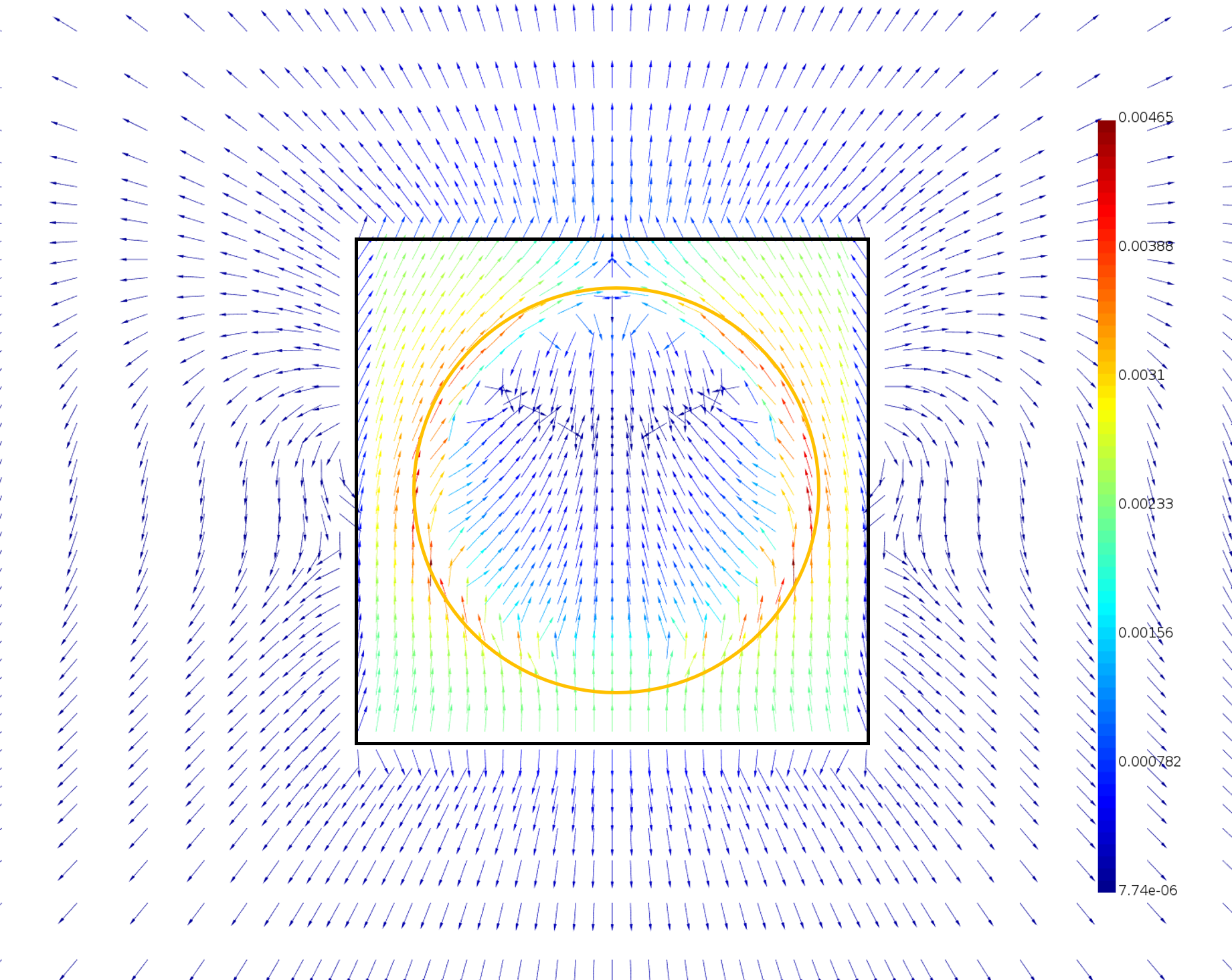
The Poynting vector shows the direction of power flow near the particle. Notice how the nanoparticle affects the Poynting vector, causing it to bend in toward the particle. Power is flowing towards the particle through the sides of the TFSF in addition to the primary injection plane. The source power calculation does not include this additional 'side power', which leads to the absorption being larger than the source power.
To reiterate, the simulation results will be correct when the TFSF source is set up as shown above. It is capable of correctly simulating the system, even when power is flowing in through the sides of the source. The only issue is that the source power normalization only accounts for the power injected from the primary injection plane, not the sides.
It is worth noting that even if the power measurements are less than 1, this is still not a very useful way to normalize the results since they depend on the source size. If the source size is doubled, the transmission data will be halved, even though the actual physical quantity (eg the power absorbed by the particle) is independent of the size of the TFSF source.
Normalized to source intensity (cross-section units)
As explained above, normalizing power measurements to the source power is not recommended. Instead, it is more meaningful to normalize power measurements to the source intensity (Watts / m^2). This returns the data a cross-section, in units of Area. To apply this normalization, simply divide the absorbed power (Watts) by the source intensity (Watts/m^2) to get the absorption cross-section in units of m^2.
It is interesting to notice that at 530nm, the absorption cross-section is larger than the geometrical area of the TFSF source, which is why the 'source power normalization' produced values larger than 1. The absorption cross-section is also much larger than the geometrical cross-section of the nanoparticle.
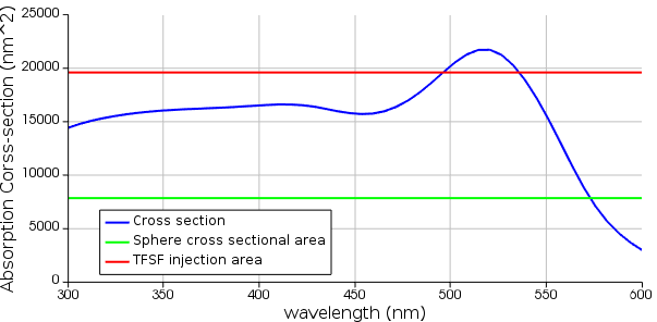
Power normalization and energy conservation
Power normalization and energy conservation with the TFSF can be non-intuitive. For example, you may find that power transmission measurements depend on the size of the source. It is also possible to find situations where power measurements are greater than 100%. While this may be non-intuitive, it is simply a normalization issue and does not indicate a simulation error. In these situations, it is usually more physically meaningful to normalize to the source intensity, rather than the power injected by the source. See the sourceintensity script function or contact Lumerical support for more information. See the Understanding source normalization in the TFSF source for additional information.
Periodic structures and the TFSF source
The plane wave source is generally the best source for periodic simulations. The TFSF source should only be used in situations where scattering in the specular (zeroeth order) direction is of interest.
The figures below show how the same structure can have different simulation outcomes when simulated using different sources, TFSF source, and plane wave source. TFSF source is used for the top cases, where the plane wave source is used for the bottom cases. The structure simulated is the same, periodic, and the FDTD simulation object employs the periodic boundary conditions, except along the axis of injection. Note that the sources extend through the FDTD simulation regions to avoid diffraction along edges.
TFSF source
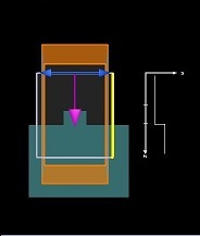
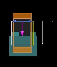
TFSF source is used in both cases. The two examples differ in the region of the structure that the TFSF source region and the FDTD simulation object are over. In the left image, the reference corner is going through the substrate, while, in the right image, the reference corner goes through the feature (assuming that the protruding part of the structure is the feature).
The subtraction happens at the boundaries of the source and the reference 1D line, which is at the top right corner of the TFSF source region (marked with the solid yellow line). As the reference corner goes through the simulation structure at different parts in these two example cases, even though the object simulated is exactly the same, the collected result of monitors outside the TFSF source region will differ.
Planewave source
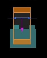
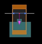
Plane-wave source is used in both cases. Both simulations will return exactly the same data.
Examples
Scattering object in free space
This is a typical setup for Mie scattering.
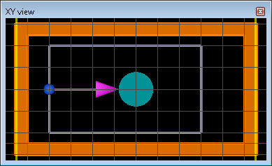
A scattering object (circle with n= 1.5) is located inside the source. Any light scattered from the object will propagate through the source boundary, into the scattered field region.
Movie of Ez(t). We can now see scattering from the circle.
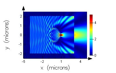
A frequency monitor records the CW fields. The electric field intensity profile is now much more complicated because of scattering from the circle. The TFSF source continues to subtract the ideal plane wave at the edge of the source. Only scattered fields will pass into the region outside the TFSF source.
Multi-layer stack with gap
The TFSF source can be used in systems with substrates and multi-layer stacks. The injection direction does not have to be normal to the surface. Also, you should extend the substrate/stack completely through the source and boundaries.
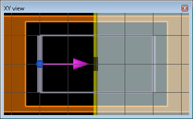
This example shows a 3 layer stack composed of Air - Gold - Glass, with a small gap in the gold layer. If you are interested in using the TFSF source with substrates or multi-layer stacks, you should first run a simulation without any gaps or scattering object, to ensure you understand the behavior of the TFSF source.
Movie of Ez(t). Notice that most of the reflection from the Gold interface is automatically removed by the injection plane of the source. Only scattering from the gap will pass through the edge of the source.
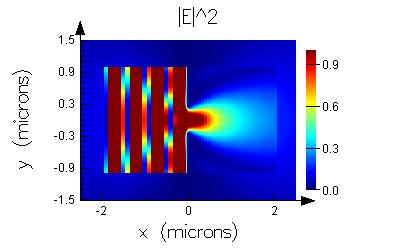
A frequency monitor records the CW fields. Once again, notice that the reflection from the Gold layer is removed by the source. Only light scattered from the gap will pass through the edge of the source.
Particle on a surface at non-normal incidence
The TFSF source can be used in systems with substrates and multi-layer stacks. This example shows how the source can be used to measure the scattering and absorption cross-sections at non-normal incidence. Please see Cross sections and normalization for details on normalization of the cross-section.

This example shows a gold particle on a surface. Note that the mesh override regions extend completely outside the source region in the x and y directions to ensure that the x and y meshes are uniform over the region of the source. The z mesh can be graded. In this example, the source and the cross-section object "scat" have been increased in size for clarity in the movie but both could be brought inside the uniform mesh override region to save memory. The source is at a nominal angle of 10 degrees, which means that the angle of incidence is actually wavelength-dependent, however, the small change in angles has been ignored in the analysis.
Movie of |E(t)|2. Notice that only the field scattered by the gold particle can be seen in the scattered field region. The light reflected by the silicon substrate is removed.
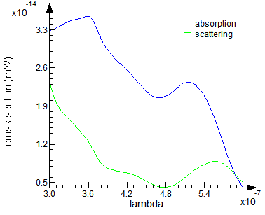

The scattering and absorption cross-sections can be calculated. A frequency monitor records the CW fields.
Absorbing materials
The TFSF source supports dispersive (absorbing) materials.
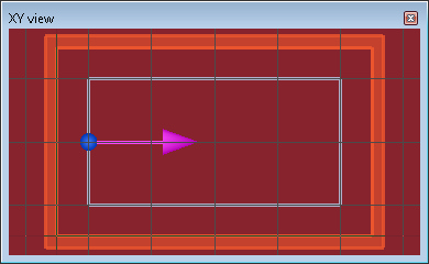
The simulation volume is composed of Silicon. At 600nm, the index of Silicon is approximately n=3.9 + i0.02, which will create substantial absorption as the fields propagate. No scattering object is present.
Movie of Ez(t).
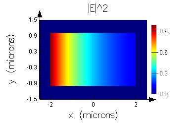
A frequency monitor records the CW fields. Notice that the field intensity decays, due to absorption. Also, notice that the fields outside the source are still zero since there is no scattering object within the source.
Understanding source normalization in the TFSF source
When using finite size beams in linear systems, we typically normalize results involving power to the power spectrum of the source. When using plane waves, which in principle have infinite power, we need to consider the scattering and absorption cross sections instead.
The cross section, s, is defined such the scattered (or absorbed) power in Watts, P, is given byP=σI
where, I
is the source intensity in Watts/m2 and the cross section has units of m2. In two dimensional simulations, which represent a structure which is infinite along the z axis, we generalize P to represent the power scattered per unit length, and the cross section has units of m.
Source power vs source intensity
By default, we normalize most power results to the power of the source. For example, the script command 'transmission' will calculate the power flux through a monitor surface and normalize to the source power, returning a dimensionless quantity. To normalize instead to the source intensity, we can use the script commands
sigma = transmission(f) * sourcepower(f) / sourceintensity(f);
where f is a vector of frequency points. The result sigma will have units of m2 from a three dimensional simulation, and m from a two dimensional simulation. For plane waves and TFSF sources, the power of the source ('sourcepower' function) is simply the intensity of the source integrated over the area of the source injection plane. Normalizing to the source intensity is particularly important for non-periodic simulations (typically involving the TFSF source), since the source power depends on the (arbitrary) size of the source as setup by the user. For more information about TFSF sources specifically, please see the Power Normalization section of TFSF tips for more details.
Angles of incidence
We have to be extremely careful about the definition of the source intensity when the source is at non normal incidence. The source intensity as returned by the script command 'sourceintensity' is calculated by integrating the power normal to the injection plane of the source. If instead, you want to normalize to the source intensity of the beam as calculated in the plane normal to the direction of propagation of the beam you need an additional factor of cos(q) where q is the nominal source angle as specified in the source properties. (Please note that this angle q should not be frequency dependent.) For example, if you download the Mie scattering example in 3D and modify the source angle to have theta of 30 degrees, you should see something like this in the yz view:
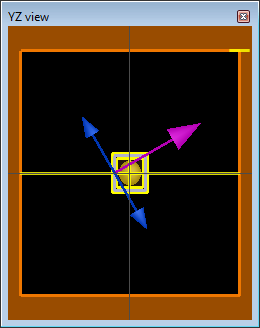
After running the simulation, we can run the usual analysis and we expect to see good agreement with the theoretical results since the scattering and absorption cross sections should not depend on angle of incidence for a sphere. Instead we will see this comparison:
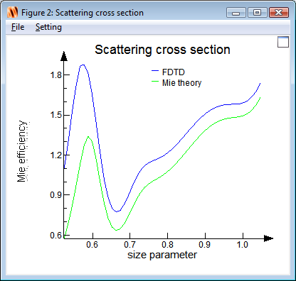
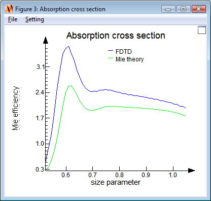
The discrepancy is mainly due to the fact that our calculation defines the source intensity, I(q) with respect to the y-normal injection plane of the source even though the source angle q is 30 degrees. The theory calculates sigma using I0, which is independent of the angle of the source. Since we know that I(q)=I0cos(q)
, we can easily modify our script by adding the lines:
theta = 30 * pi/180; # the nominal source angle is 30 degrees
Qscat = Qscat * cos(theta);
Qabs = Qabs * cos(theta);
immediately after calculating the cross section. (Please note that q is the nominal source angle and does not have to be corrected for wavelength.) We then see the results below, which are as accurate as the normal incidence results on this 5nm mesh, and converge nicely as the mesh size becomes smaller.
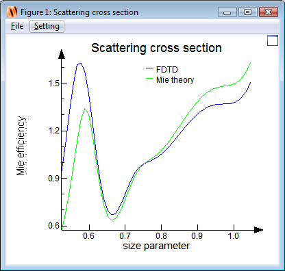
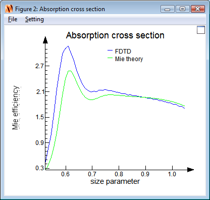
| Note: The Mie scattering example considered here is a very particular case where the dependence of the angle of injection on wavelength does not affect the results. This is a consequence of the cross section of a sphere being independent of the injection angle. For other geometries without this symmetry, it is necessary to bear in mind that the TFSF source has the same issues as the plane wave source for Plane waves - Angled injection . This problem must be considered in addition to the normalization correction described here. |
Periodic structures
In periodic structures, simulated with periodic or Bloch boundary conditions, the source power is integrated over one unit cell. This makes it possible to discuss quantities such as reflected power and transmitted power as fractions of the source power, as we do with finite sized beams. However, we should remember that this can be easily converted into a cross section. For example, a periodic structure with a reflection of 25% simply means that the reflection cross section is 25% of the unit cell area.
Structures on multi-layer stacks or substrates
We must pay special attention to the meaning of the scattering and absorption cross sections when the particle is on or in a substrate or multi-layer stack. If the substrate is absorbing, then the box that measures the absorption cross section of the particle must surround only the particle. If that is not possible, then the loss per unit volume must be integrated only over the particle volume. The scattering cross section is more subtle: since the incident field is defined as the field that would exist in the multi-layer in the absence of the defect, the scattering cross section will not include any power from the specular reflection or transmission. This is ideal for detecting small scattering cross sections on surfaces that have large specular reflections. However, in the precise direction of the specular reflection it will not be possible to directly measure the simulated result since experimentally the specular reflection will dominate the small scattering from the defect. Please see the TFSF tips section for an example of setting up this type of simulation.
| Note : Since BFAST assumes periodic structure, users should not use BFAST source at an angle to replace TFSF to get oblique incidence result. |
Mode source - Simulation object
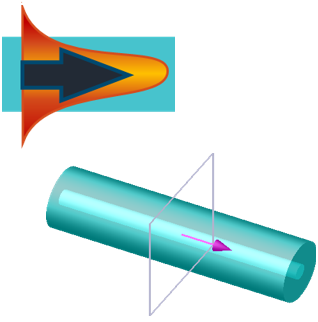 The mode source is used to inject a guided mode into the simulation region. The geometry of the mode source (i.e. center location, and span) is used to compute the guided modes for the structure. In three-dimensional simulations, the modes are computed across a plane, while in two-dimensions they are computed across a line. From a list of possible modes, a single mode is selected for injection into the simulation region.
This section describes the operation of the integrated mode solver to inject guided waves into FDTD simulations or the Propagator in MODE. The mode solver itself uses the same discretization mesh as the FDTD/propagator algorithm, so the profile of the guided modes as computed with the mode solver naturally interface with the underlying FDTD/propagator mesh. Overall, this facilitates the injection of guided modes with minimal back-reflection.
By default, this source will inject the fundamental mode (the mode with the largest effective index). You can control the polarization of the automatically selected mode by setting the MODE SELECTION field to fundamental TE or TM. With these settings, the mode source will automatically update the mode profile as the structure is modified. This can be very helpful for tasks such as parameter sweeps where the waveguide geometry is changed.
Alternatively, it is possible to select an arbitrary mode by setting MODE SELECTION to "user select". In this case, the integrated mode solver is launched by pressing the SELECT MODE button within the mode source edit window.
| Note: Mode selection - "user select"
|
| Note: Choosing polarization if varFDTD In varFDTD, the polarization of the mode source is determined by the polarization of the slab mode you choose in the Effective index tab of the simulation region object. The polarization of the mode source should matches that of the slab mode. |
| Note: Broadband simulations By default, the Mode source calculates the spatial mode profile at one frequency point, which is the center frequency of the specified frequency range, then injects that mode profile at all frequencies. This method keeps the mode profile calculation computationally inexpensive. This approach works very well for single frequency and narrowband simulations as the injection errors are very low at the center frequency, but they grow larger with distance due to the mode profile mismatch. Therefore, it is recommended to use multiple frequency points for broadband simulation in order to reduce the injection error. For more information, see Mode source - Broadband |
General
- INJECTION AXIS: Sets the axis along which the mode source will propagate.
- DIRECTION: This field specifies the direction in which the TFSF source propagates. FORWARD corresponds to propagation in a positive direction, while BACKWARD corresponds to propagation in a negative direction.
- AMPLITUDE: The amplitude of the mode source as explained in the Units and normalization section.
- PHASE: The phase of the point source, measured in units of degrees. Only useful for setting relative phase delays between multiple radiation sources.
- MODE SELECTION: Defines whether to inject fundamental mode or other user-selected mode chosen via the "Select Mode" button.
- SELECT MODE: Mode source only. Launches the mode solver and allows the user to select the desired mode for injection. For more information on using the mode source, consult the mode analysis section.
- VISUALIZE DATA: Opens a visualizer to show the mode profile of the currently selected mode. If multifrequency mode calculation is enabled, the slider can be used to visualize the mode profile at various frequency points.
- CLEAR DATA: Clears the selected mode for mode sources, or clears the imported data for imported sources
- NUMBER OF TRIAL MODES: The number of modes specified to look for in order to find a fundamental mode. This will affect the modes that the solver finds. If this number is too small, the desired modes may not be found. Often, setting this number to 100 modes will ensure that no physical modes have been missed. If more than 100 modes exist, then a larger number should be used if one is interested in higher-order modes.
- MULTIFREQUENCY MODE CALCULATION: Used for broadband simulations, this option enables mode profile calculations at n frequency points
- FREQUENCY POINTS: Specifies the number of frequency points between the start and stop frequency at which the mode profile will be calculated to minimize mode mismatch error
- BENT WAVEGUIDE: Calculates the mode profile for a waveguide with a bent specified by radius and orientation as described in this article.
- BEND RADIUS: Sets the bend radius for bent waveguide calculation
- BEND ORIENTATION: Sets the bend orientation for bent waveguide calculation(e.g. to define whether the waveguide bends in XZ or XY plane)
- THETA: In 3D simulations, this is the angle of propagation, in degrees, with respect to the injection axis of the source. In 2D simulations, it is the angle of propagation, in degrees, rotated about the global Z-axis in a right-hand context, i.e. the angle of propagation in the XY plane.
- PHI: In 3D simulations, this is the angle of propagation, in degrees, rotated about the injection axis of the source in a right-hand context. In 2D simulations, this value is not used.
- OFFSET: Allows users to set an offset to the plane where the mode is calculated. This is useful for ensuring that mode sources at an angle do not intersect with structures that are not part of the waveguide/fiber.
Geometry
The geometry tab contains options to change the size and location of the sources.
Frequency/Wavelength
The Frequency/Wavelength tab is shown below. This tab can be accessed through the individual source properties or the global source properties. Note that the plots on the right-hand side of the window update as the parameters are updated, so that you can easily observe the wavelength (top figure), frequency (middle figure), and temporal (bottom figure) content of the source settings.

At the top-left of the tab, it is possible to chose to either SET FREQUENCY / WAVELENGTH or SET TIME-DOMAIN. In most simulations, the 'SET FREQUENCY / WAVELENGTH ' option is recommended.
If you choose to directly modify the time domain settings, please keep the following points in mind:
- PULSE DURATIONS: Choose a pulse duration that can accurately span your frequency or wavelength range of interest. However, very short pulses contain many frequency components and therefore disperse quickly. As a result, short pulses require more points per wavelength for accurate simulation.
- PULSE OFFSET: This parameter defines the temporal separation between the start of the simulation and the center of the input pulse. To ensure that the input pulse is not truncated, the pulse offset should be at least 2 times the pulse duration. This will ensure that the frequency distribution around the center frequency of the source is close to symmetrical, and the initial fields are close to zero at the beginning of the simulation.
- SOURCE TYPE: In general, you can choose between ‘standard’ and ‘broadband’ source types. Standard sources consist of a Gaussian pulse at a fixed optical carrier, while the broadband sources consist of a Gaussian pulse with an optical carrier which varies across the pulse envelope. Broadband sources can be used to perform simulations in which wideband frequency data is required – for instance, from 200 to 1000 THz. This type of frequency range cannot be accurately simulated using the standard source type.
Set frequency wavelength
If the SET FREQUENCY / WAVELENGTH option was chosen, this section makes it possible to either set the frequency or the wavelength and choose to either set the center and span or the minimum and maximum frequencies of the source.
For single frequency simulations, simply set both the min and max wavelengths to the same value.
Set time domain
The options in the time domain section are:
- SOURCE TYPE: This setting is used to specify whether the source is a standard source or a broadband source. The standard source consists of an optical carrier with a fixed frequency and a Gaussian envelope. The broadband source, which contains a much wider spectrum, consists of a chirped optical carrier with a Gaussian envelope. When the user uses the script function setsourcesignal, this field will be set as "user input".
- FREQUENCY: The center frequency of the optical carrier.
- PULSE LENGTH: The full-width at half-maximum (FWHM) power temporal duration of the pulse.
- OFFSET: The time at which the source reaches its peak amplitude, measured relative to the start of the simulation. An offset of N seconds corresponds to a source which reaches its peak amplitude N seconds after the start of the simulation.
- BANDWIDTH: The FWHM frequency width of the time-domain pulse.
For more information, please visit Changing the source bandwidth
Advanced
- ELIMINATE DISCONTINUITY: Ensures the function has a continuous derivative (smooth transitions from/to zero) at the start and end of a user-defined source time signal. Enabled by default.
- OPTIMIZE FOR SHORT PULSE: Use the shortest possible source pulse.
- This option is enabled by default in the FDTD solver. It should only be disabled when it is necessary to minimize the power injected by the source that is outside of the source range (eg. convergence problems related to broadband steep angled injection).
- This option is disabled by default in the varFDTD solver, as it improves the algorithm's numerical stability.
- ELIMINATE DC: Eliminates the DC component by forcing signal symmetry
Manual calculation of the source time signal
As explained above, the 'Standard' source type uses a fixed carrier with a Gaussian envelope. The following script code shows how to calculate the source time signal used by the source.
# calculate standard pulse time signal
frequency  = 300e12;
pulselength = 50e-15;
offset   = 150e-15;

t      = linspace(0,600e-15, 10000);
w_center  = frequency*2*pi;
delta_t   = pulselength/(2*sqrt(log(2)));
pulse = sin( -w_center*(t-offset)) * exp( -(t-offset)^2/2/delta_t^2 );

plot(t*1e12,pulse,"t (fs)","source pulse time signal");
| Note : There are some small differences between the pulse generated by this code and the actual time signal generated by the 'standard' source pulse setting. If you need very precise control over or knowledge of the source time signal, you should create your own Custom time signal. The 'broadband' option is generated with a more complex function. The precise function is not provided. To create your own arbitrary source time signals, see the Custom time signal page. |
Results
- NEFF: Effective index as a function of frequency/wavelength is returned.
- MODE PROFILES: Mode profiles (E, H, and index) are returned as a function of position and frequency/wavelength.
- TIME SIGNAL: Time-domain signal of the source pulse.
- SPECTRUM: The Fourier transform of the time signal.
Mode source - Mode analysis - Simulation Object
 The MODE ANALYSIS window is shown in the screenshot below. The upper portion of the window contains the MODE LIST where the mode number, effective index, propagation loss, and polarization are shown. The lower left-hand corner shows the calculation parameters; upon launch, the lower left-hand portion of the window shows the default calculation parameters to be used to simulate the structure. The right-hand portion of the window contains the PLOT AREA where the simulation data is plotted, and the two drop-down boxes at the top of the plot area are used to specify which data to plot in the plot window, while the region at the bottom right can be used to modify the current mode plot options. Upon launch, the plot area shows the refractive index profile of the structure being analyzed.
Modal analysis tab
The modal analysis portion of the window displays simulation data relevant to the different modes calculated for the structure of interest. This portion of the window shows the modes, arranged from top to bottom in terms of the highest effective index and numbered sequentially. For each mode, this portion of the window shows the effective index of the mode, the calculated loss (measured in dB per millimeter of propagation; only valid for lossy materials), and the polarization fraction (please see Mode List and Deck for the full definition).
Boundary conditions tab
The boundary conditions that are supported by FDTD and MODE are listed below.

Perfectly matched layer (PML)1 boundaries absorb electromagnetic waves incident upon them. They essentially model open (or reflectionless) boundaries. In FDTD and varFDTD simulation regions, the user can directly specify all the parameters that control their absorption properties including the number of layers. To facilitate the selection of PML parameters, a number of profiles (or predefined sets of parameters) are available under the boundary conditions tab. In most simulation scenarios, the user only needs to choose one of the predefined profiles and fine tune the number of layers. PML boundaries perform best when the surrounding structures extend completely through the boundary condition region. This will be the default behavior of structures whether or not they were drawn to end inside or outside the PML region.
1 J. P. Berenger, Perfectly Matched Layer (PML) for Computational Electromagnetics. Morgan & Claypool Publishers, 2007.

Metal boundary conditions are used to specify boundaries that behave as a Perfect Electric Conductor (PEC). The component of the electric field parallel to a metal (PEC) boundary is zero; the component of the magnetic field H perpendicular to a metal (PEC) boundary is also zero. Metal boundaries are perfectly reflecting, allowing no energy to escape the simulation volume along that boundary. In the FDE solver, metal BC is the default setting.

PMC
Perfect Magnetic Conductor (PMC) boundary conditions are the magnetic equivalent of the metal (PEC) boundaries. The component of the magnetic field H parallel to a PMC boundary is zero; the component of the electric field perpendicular to a PMC boundary is also zero.

Periodic BC should be used when both the structures and EM fields are periodic. Periodic boundary conditions can be used in one or more directions (i.e. only in the x direction) to simulate a structure which is periodic in one direction but not necessarily other directions.

Bloch BC should be used when the structures and the EM fields are periodic, but a phase shift exists between each period. Bloch boundary conditions are used in FDTD and propagator simulations predominantly for the following two simulations:
- Launching a plane wave at an angle to a periodic structure – in this situation, accurate reflection and transmission data can be measured at a single frequency point for a given simulation.
- Calculating the bandstructure of a periodic object – in this situation, a broadband pulse is injected via a dipole source into a periodic structure.
| Note: if you choose BFAST plane wave source, the Bloch BCs will be automatically overridden and use its built_in boundary conditions. |


Symmetric / Anti-Symmetric
Symmetric/anti-symmetric boundary conditions are used when the user is interested in a problem that exhibits one or more planes of symmetry; both the structure and source must be symmetric. Symmetric boundaries are mirrors for the electric field, and anti-mirrors for the magnetic field. On the other hand, antisymmetric boundaries are anti-mirrors for the electric field, and mirrors for the magnetic field. Careful consideration must be given to whether symmetric or anti-symmetric boundary conditions are required, given the vector symmetry of the desired solution. For meaningful results, the sources used must have the same symmetry as the boundary conditions. Further information about symmetric and anti-symmetric boundary conditions can be found in Choosing between symmetric and anti-symmetric BCs.
ALLOW SYMMETRY ON ALL BOUNDARIES: Allows symmetric boundary conditions with periodic structures (this option is not available in the boundary condition tab of mode sources and mode expansion monitors).
Select Mode
Pressing this button (located on the lower right corner of the window) will initialize the mode source with the current mode selected within the mode table in the upper left-hand portion of the window.
Advanced Options
The ADVANCED OPTIONS button (located on the lower left corner of the window) brings up the "Mode Advanced Options" window with the following parameters:
- CONVERGENCE TOLERANCE: the convergence tolerance used for the calculations. The default value corresponds to 1e-12 but can be increased by the user to speed convergence or decreased to improve accuracy.
- MAXIMUM NUMBER OF MODES TO STORE: When searching for modes in a range of effective indices from n1 to n2, it is possible to fill your available memory if too many modes are found. For this reason, the maximum number of modes is limited and the calculation will stop when this number of modes is exceeded.
- USE SINGLE PRECISION: this can be used to save some memory during the calculation of the modes but the results are less accurate.
| Note: Default boundary conditions (BC) in Mode solver By default, the integrated mode solver uses Metal BC's, except in the following situations.
In the Boundary conditions tab you can override these default settings to select PML or PMC boundary conditions. |
Mode source - Plot and analysis options - Simulation Object
 The plot and analysis windows are shown in the screenshot below.
The left portion of the window displays the calculation parameters:
- FREQUENCY: the frequency at which the modes are solved for.
- WAVELENGTH: the wavelength at which the modes are solved for.
- NUMBER OF TRIAL MODES: the number of modes to be calculated.
- SEARCH: this pull-down allows the user to specify which option to search for modes in, the available options are:
- NEAR N: Allows you to look for modes near a desired effective index.
- USE MAX INDEX: Search for modes near the maximum index found in the meshed cross section.
- N: Choose the effective index to search for. - IN RANGE: Allows you to search for modes in a desired range of indices.
- N1, N2: Define the range of indices to search over.
- NEAR N: Allows you to look for modes near a desired effective index.
- BENT WAVEGUIDE: Allows the user to specify a current radius of curvature for the mode and solver for the modes of a bent waveguide. See Bent waveguide calculation for a more detailed description.
- BEND RADIUS: the bend radius of the waveguide measured from the center of the mode solver region
- BEND ORIENTATION: the orientation of the radius of curvature.
- CALCULATE MODE: by clicking this button the mode solver will start the calculation for the waveguide modes given the criteria above.
- RESTORE LAST SETTINGS: restores the calculation parameters to the current simulation parameters corresponding to the modes that have been calculated.
Figure window
The plot itself where the data appears is automatically labeled and scaled to fit the simulation data. As with the layout editor, the plot can be zoomed using the standard mouse actions. Note, however, that the mouse is automatically in the zoom state when over the plotted data and therefore the keyboard shortcut Z is not necessary.
Mode plot options
The MODE PLOT OPTIONS can be set in the bottom right of the MODE ANALYSIS window, the options are
- PLOT: This pull-down allows the user specifies what simulation data should be plotted within the plot area.
Box 1 specifies what general class of data to plot:
-
- MODAL FIELDS: allows the user to select various field quantities such as electric and magnetic field amplitudes and intensities and Poynting vectors using the COMPONENT pull-down
- MATERIAL PROPERTIES: allows the user to select various physical quantities such as refractive index, permittivity, and conductivity using the COMPONENT pull-down
Box 2 specifies which part of complex-valued simulation data is to plot:
-
- AMPLITUDE
- PHASE
- REAL PART
- IMAGINARY PART
- COMPONENT: This pull-down allows the user to specify which specific component is to be plotted within the plot area. The available options depend on the setting of the PLOT pull-down.
- COORDINATES: currently supports only the CARTESIAN coordinate system.
- LINEAR/LOG SCALE: determines whether the simulation data is plotted on a linear or a log plot
- SUPERIMPOSE STRUCTURE: toggles whether a black outline showing the physical structure is superimposed on the simulation data
Tips for finding modes with the mode source
When using the eigensolver in MODE or the mode source in FDTD, there are many eigensolver settings that can affect the modes found. For some types of structures, finding the correct modes can be challenging. This page provides a checklist of common settings that should be checked or modified when you have trouble finding the right modes or you get the message "no physical modes were found".
Simulation boundaries
It is often recommended that one starts with metal boundaries when looking for well confined modes. Please see Starting with metal boundary conditions for detailed information. If the right boundaries are not chosen, the right modes may not be found. The size of the simulation region is also important. When using metal boundaries, the boundaries should be far enough from the structure interfaces so that the evanescent tails of the modes do not reach the boundaries and get reflected.
If the mode you are interested in is radiative, you will need to use PML boundaries. Please see Lossy modes and dB/m to k conversion for more information.
| Note: The Integrated Mode Source When finding modes in the Mode Source, the default boundaries are metal. These boundary conditions can be changed as explained here. |
Symmetry
Enforcing symmetry in one or two directions can greatly reduce the simulation time and memory; however, one should use these boundaries with care when solving for modes. Depending on the type of boundary used, symmetric or anti symmetric, only TE or only TM results could survive. Make sure you know the symmetry of the fields you are looking for before you apply symmetry boundaries. Please see Symmetry boundary conditions for detailed information on how to determine which symmetry boundary to use.
When using symmetry, sometimes it is necessary to "force symmetry" on the mesh as well. This option can be selected under the "advanced options" tab of the simulation region object.
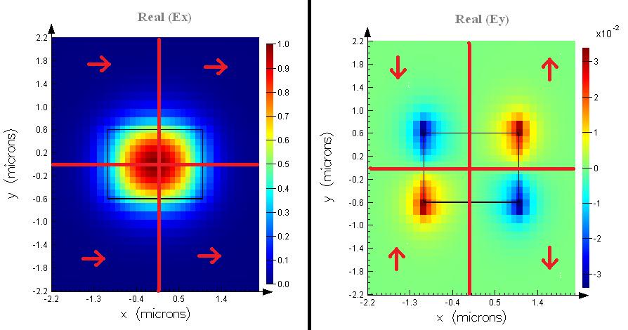
Index to search near
One can specify the index to search near or a range of indices to search in between for modes of interest. The specified value is not just the real part of the index, rather it is the magnitude of the complex index.
If the mode is lossy, you may want to enter a complex value for this index. Please see Lossy modes and dB/m to k conversion for more information.
For the RF frequency range, if the structure is open (eg. transmission line embedded in free space):
- If the mode is guided, the guess index should be greater than or equal to the background index
- If the mode is radiating, the guess index should be less than or equal to the background index
If the structure is closed (eg. a hollow metallic waveguide):
- For frequencies near the mode's cutoff frequency, the guess index should be much less than the background index
- For frequencies away from the cutoff frequency, the guess index should be less than or equal to the background index
Number of trial modes
The number of modes specified to look for around a refractive index value will affect the modes that the solver finds. If this number is too small, the desired modes may not be found. Often, setting this number to 100 modes will ensure that no physical modes near the specified index have been missed. If more than 100 modes exist, then a larger number should be used if one is interested in higher order modes.
Mode source in broadband simulations
This topic describes how the Mode source operates in broadband time-domain simulations, and how to significantly reduce the injection errors that can occur due to the mode mismatch.
Introduction
The mode solver of the Mode source uses a frequency domain technique to calculate the modes of a structure. This technique is inherently single frequency and if the default source settings is used, the mode solver calculates the mode profiles at the center frequency of the source. For example, if the source range is 300-600 THz, the mode solver will calculate the modes at 450 THz. If the mode profile is relatively constant as a function of frequency, this works well. However, if the mode profile changes over the specified frequency range, there will be some reflection and scattering at the source injection plane. This can be understood in terms of the mode profile mismatch between the mode that actually exists at that frequency and the mode profile of the center frequency that is being injected. These errors will be most noticeable at the minimum and maximum frequencies where the mode mismatch is largest.
Broadband Simulation Settings - FDTD
To significantly reduce the mode mismatch errors for broadband simulations, multi-frequency calculation can be enabled as shown on figure 2. Enabling this settings allows to specify the number of frequency points at which the mode profile will be calculated. The frequency points lie within the start-stop frequency range and they are located at the Chebyshev grid(rather than being linearly distributed within the start-stop range). The mode profiles at each frequency point can be displayed in the visualizer by clicking on the "Visualize Data" button as shown on figure 3.
|
Mode source settings |
Mode profiles calculated at the frequency points specified in the source settings
Actually injected frequency dependent fields in log scale |
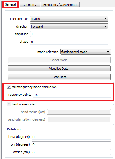
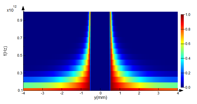
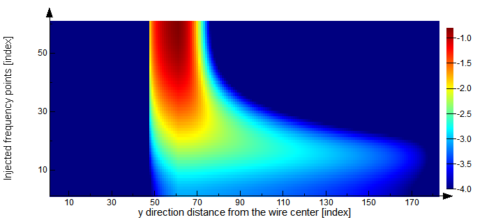
Number of Frequency Points, Accuracy and Performance Considerations
When setting up the number of frequency points for a broadband mode source simulations, it is important to realize that the frequency points do not represent the fields that are actually injected into the simulation. The injected, frequency dependent fields are obtained by interpolating the function at the specified frequency points during the simulation initialization. Since the points are located on Chebyshev grid, the interpolation can be very precise even with fairly small amount of points depending on the function smoothness. As a result, adding large number of frequency points can increase the simulation time without any considerable gains in accuracy. Therefore, it is recommended to start with a smaller number of frequency points and conduct convergence testing. An example to demonstrate this behavior is shown on the mode profiles above at the specified frequency points and the actual injected fields.
Example
To demonstrate the multifrequency calculation feature, we will use an example of a copper wire with thin dielectric coating operating in broadband THz range. The theory tells us that the pulse propagates along the wire as a surface wave and produces a chirped signal. Additionally, since the dielectric coating causes the injected mode to be dispersive, the mode profile changes drastically with frequency. As such, this example can nicely demonstrate the advantages of multifrequency calculation feature for broadband simulations with mode source. The simulation setup is using three time monitors to record the time profile of the pulse right after the injection and after it propagates along 40 mm of the coated wire surface. The distance of 4 cm is chosen intentionally to allow us to compare the results with the reference paper that includes experimental and analytical results. The third monitor behind the source allows us to observe the amount of back-scattering.
To run the example, open the simulation file broadband_mode_source_thz_wire.fsp and run the associated script broadband_mode_source_thz_wire.lsf. The script will run one simulation in a single frequency mode and then it will repeat the same simulation with multifrequency calculation turned on and 15 frequency points. The movie shown in figure 5 represents the single frequency simulation. It can be clearly seen that there is considerable amount of back-scattering during the injection and the initial pulse propagation demonstrates interference due to the mode mismatch. As opposed to that, the movie in figure 6 shows that the multifrequency mode calculation significantly decreases the back scattering and the propagation along the wire surface produces nice clean chirped signal.
The advantage of the broadband mode source is also very clear when we compare the time profiles of the injected and propagated pulse. The multifrequency simulation results captured in figure 8 show that the time domain profile(Ey fields) of the injected pulse is cleaner and the dispersion creates a chirped signal that is very well aligned with the analytical and experimental results.
| Single frequency mode source calculation | Multifrequency mode source calculation |
| Field of the injected and propagated pulse with single frequency calculation | Field of the injected and propagated pulse with multi-frequency calculation |
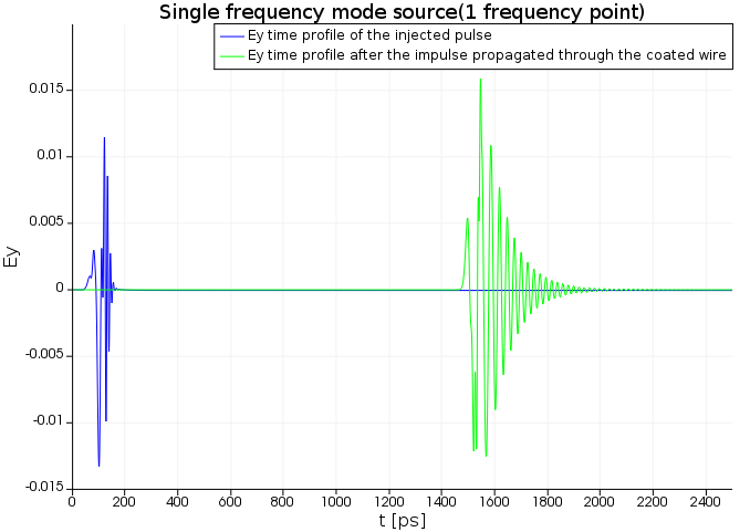
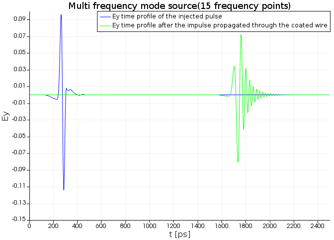
Broadband Simulation in varFDTD
The mode solver of the Mode source in varFDTD does not feature the multifrequency calculation option. Therefore, the behavior of the mode source is ideal for single frequency simulations, but creates a potential problem for broadband simulations. As noted above, the mode solver calculates the mode profile at the center frequency of the source range. The selected mode profile will then be injected over the entire frequency range of the source, which can result in injection and back-scattering errors. To avoid these errors in varFDTD, it might be necessary to use a smaller source bandwidth in order to minimize these problems. Unfortunately, if you need to collect broadband data, this means you will have to run multiple simulations, which will increase the overall simulation time.
Injecting modes at an angle with the mode source
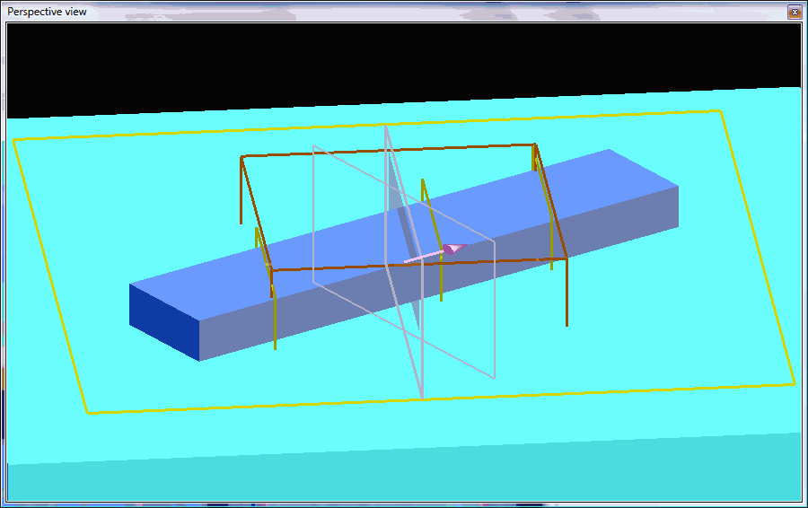 This topic explains how the Mode source works when injecting into waveguides at non-normal incidence and how the multifrequency mode profile calculation can benefit angled injection in broadband simulations.
Features
The Mode source can be configured to inject at an angle, just like the plane wave and gaussian beam sources. The additional complication with the Mode source is that there are two planes of interest:Source Configuration
1) Before the main FDTD simulation is run, the mode source must use it's built-in mode eigensolver to calculate the supported modes of the waveguide. This calculation requires a cross section of the waveguide normal to the waveguide propagation direction. This plane is drawn in the CAD with a white outline.
2) During the actual FDTD simulation, the source must inject along one of the global simulation axes (x,y, or z). This plane is shown in the CAD as a shaded plane with a while outline.
|
Mode profile calculation and injection planes |
Rotations and multifrequency calculation settings |
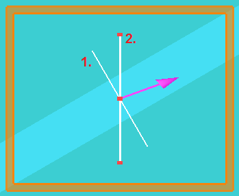
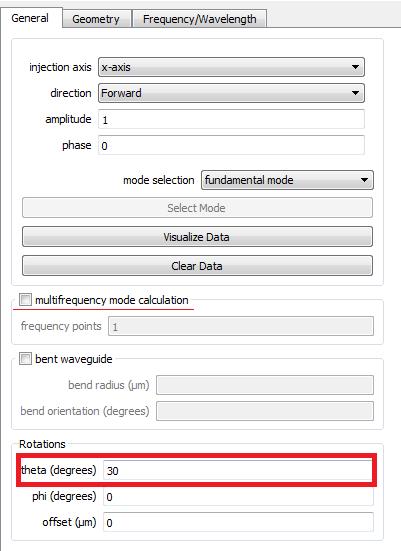
Angled Injection and Broadband Simulations
It is matter of fact that the injected fields have constant in-plane wavevector at all frequencies. The in plane wave vector is chosen such that the actual injection angle at the center frequency of the simulation matches the nominal injection angle. Since the magnitude of the wavevector is proportional to frequency, the actual injection angle will change as a function of frequency. Higher frequencies will be injected at smaller angles, while lower frequencies will be injected at larger angles as explained here.
To avoid this problem, multifrequency mode calculation can be enabled in order to update the properties of the injected fields at specified frequency points and keep the injection angle constant across the simulation bandwidth. To demonstrate this, we have modified the simulation file above to inject wavelengths from 800nm to 1200nm. If the default single frequency calculation is used, the injection angle will be calculated for the center frequency of 1000nm. Figure 3 shows that the longer wavelengths are injected at steeper angle and the light bounces from the waveguide walls. Figure 4 then shows the same wavelength with the multifrequency calculation on. It is apparent that the injection angle error is eliminated.
|
Injected fields at 1200nm for a simulation with center wavelength at 1000nm and single frequency mode profile calculation |
Injected fields at 1200nm for a simulation with center wavelength at 1000nm and multifrequency mode profile calculation |
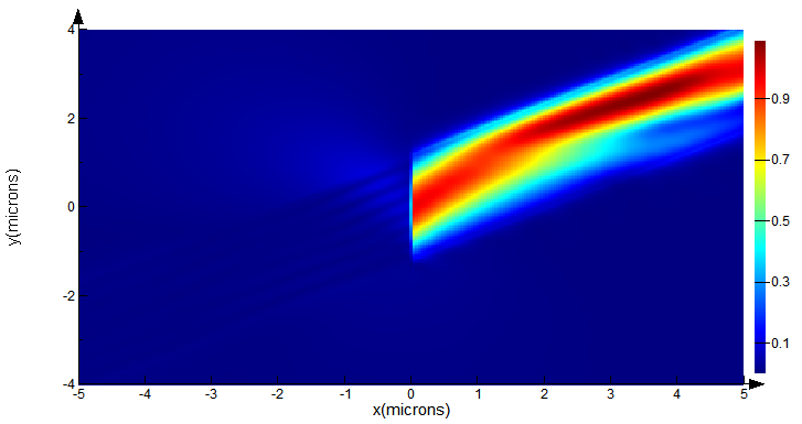
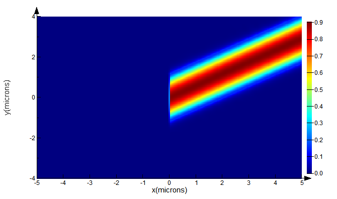
Import source - Simulation object
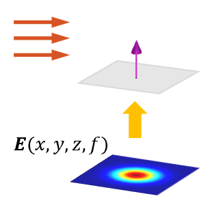 The import source allows the user to specify a custom spatial field profile for the source injection plane. The custom field profile can be calculated from an analytic formula, imported from another FDTD simulation, or from other simulation tools.
Import dataset format
The 2D cross section of field data to be imported must be saved in a lumerical dataset with the format shown below. Note that E and H fields can be complex valued and non-uniform spatial sampling is supported. The E-fields are required, but the H-fields are optional.
EM = rectilineardataset("EM fields",x,y,z);
EM.addparameter("lambda",c/f,"f",f); # Optional
EM.addattribute("E",Ex,Ey,Ez);
EM.addattribute("H",Hx,Hy,Hz);       # Optional
Specifying magnetic fields
The magnetic H fields are optional. If the H fields are not supplied, the source will attempt to calculate the H fields from the E fields. This calculation makes certain assumptions about the change of phase of the propagating radiation. These assumptions hold true for narrow sources such as Gaussian and plane wave sources, but may lead to significant errors for other sources with more complex field profiles. When defining complex beams, it is best to specify both E and H.
In some situations, it is useful to include H in the source dataset, but to set the value to the fields to zero. This can be interpreted as a situation where the same beam is propagating in both the forward and the backward direction at the same time, oriented such that the E fields interfere constructively at the source plane and the H fields interfere destructively. This technique is a useful way to avoid manually calculating the H fields. Instead, the H fields are naturally calculated as the fields propagate through the simulation volume. While this technique can be helpful, it is important to take some additional care when analyzing results from this type of simulation. There are two main issues:
- Fields will be injected in both the forwards and the backwards direction. This is usually not a serious problem. If the simulation is setup properly, with no structure behind the source, these fields will simply be absorbed by the PML boundaries behind the source without creating any errors in the rest of the simulation.
- The automatic calculation of the amount of power injected by the source (ie. sourcepower script function) will not be correct. Therefore, power transmission data ('T' in the result view, and results from the 'transmission' script function) which is normalized to the sourcepower, will be incorrect. A work around is to manually calculate the sourcepower and power transmission data.
Broadband simulations
The improved Mode and Import sources introduced in 2017a and later releases offer the possibility to be used in broadband simulations by enabling multi-frequency calculation that allows injection of frequency dependent mode profiles. To learn more more about the difference between single and multi-frequency mode profile calculation, see Mode source - Broadband.
In case of import source, the multifreqency calculation is enabled by simply importing 3D rectilinear dataset that contains 2D cross section of field data at multiple frequency points(third dimension). This feature is also supported by the frequency domain field and power monitors that record field data at multiple frequency points and can be easily saved into a mat file.
Note that the best accuracy with minimum number of frequency points is achieved when the points are sampled onto Chebyshev grid. If the frequency points are located outside of the Chebyshev grid, there might be some interpolation error or it might be necessary to use more points to achieve comparable accuracy.
For certain cases, where the field changes rapidly as a function of frequency, the multi-frequency method can result in interpolation error even with a large number of frequency points, so it is important to test the source in free space to ensure that the injected field profile is as-expected.
| Note: 2D simulations To use the import source in a 2D simulation, the imported field data should be 1D. In other words, two of the three dimensions in the dataset (x, y, z) should have a size of one. |
General tab
- AMPLITUDE: The amplitude of the source as explained in the Units and normalization section.
- PHASE: The phase of the point source, measured in units of degrees. Only useful for setting relative phase delays between multiple radiation sources.
- INJECTION AXIS: Sets the axis along which the radiation propagates. Automatically defined based in imported data.
- DIRECTION: This field specifies the direction in which the radiation propagates. FORWARD corresponds to propagation in the positive direction, while BACKWARD corresponds to propagation in the negative direction.
- IMPORT SOURCE: Button to load field profile from a dataset contained within a .mat or Zemax zbf file. The legacy .fld file format is also supported. Alternately, the importdataset script command can be used to load data into the source while using a script. See above for details on the dataset format.
- IMPORTED SOURCE SETTINGS: x0, y0, z0, imported wavelength: The x,y,z spatial center of the imported data, and the imported wavelength (optionally included in the imported data).
Geometry tab
The geometry tab contains options to change the size and location of the sources. The source span will be automatically set based on the imported field data.
Frequency/Wavelength tab
The Frequency/Wavelength tab is shown below. This tab can be accessed through the individual source properties, or the global source properties. Note that the plots on the right-hand side of the window update as the parameters are updated, so that you can easily observe the wavelength (top figure), frequency (middle figure) and temporal (bottom figure) content of the source settings.

- PULSE DURATION: Choose a pulse duration that can accurately span your frequency or wavelength range of interest. However, very short pulses contain many frequency components and therefore disperse quickly. As a result, short pulses require more points per wavelength for accurate simulation.
- PULSE OFFSET: This parameter defines the temporal separation between the start of the simulation and the center of the input pulse. To ensure that the input pulse is not truncated, the pulse offset should be at least 2 times the pulse duration. This will ensure that the frequency distribution around the center frequency of the source is close to symmetrical, and the initial fields are close to zero at the beginning of the simulation.
- SOURCE TYPE: In general, you can choose between ‘standard’ and ‘broadband’ source types. Standard sources consist of a Gaussian pulse at a fixed optical carrier, while the broadband sources consist of a Gaussian pulse with an optical carrier which varies across the pulse envelope. Broadband sources can be used to perform simulations in which wideband frequency data is required – for instance, from 200 to 1000 THz. This type of frequency range cannot be accurately simulated using the standard source type.
Set frequency wavelength
If the SET FREQUENCY / WAVELENGTH option was chosen, this section makes it possible to either set the frequency or the wavelength and choose to either set the center and span or the minimum and maximum frequencies of the source.
For single frequency simulations, simply set both the min and max wavelengths to the same value.
Set time domain
The options in the time domain section are:
- SOURCE TYPE: This setting is used to specify whether the source is a standard source or a broadband source. The standard source consists of an optical carrier with a fixed frequency and a Gaussian envelope. The broadband source, which contains a much wider spectrum, consists of a chirped optical carrier with a Gaussian envelope. When the user uses the script function setsourcesignal, this field will be set as "user input".
- FREQUENCY: The center frequency of the optical carrier.
- PULSE LENGTH: The full-width at half-maximum (FWHM) power temporal duration of the pulse.
- OFFSET: The time at which the source reaches its peak amplitude, measured relative to the start of the simulation. An offset of N seconds corresponds to a source which reaches its peak amplitude N seconds after the start of the simulation.
- BANDWIDTH: The FWHM frequency width of the time-domain pulse.
For more information, please visit Changing the source bandwidth
Advanced
- ELIMINATE DISCONTINUITY: Ensures the function has a continuous derivative (smooth transitions from/to zero) at the start and end of a user-defined source time signal. Enabled by default.
- OPTIMIZE FOR SHORT PULSE: Use the shortest possible source pulse.
- This option is enabled by default in the FDTD solver. It should only be disabled when it is necessary to minimize the power injected by the source that is outside of the source range (eg. convergence problems related to broadband steep angled injection).
- This option is disabled by default in the varFDTD solver, as it improves the algorithms numerical stability.
- ELIMINATE DC: Eliminates the DC component by forcing signal symmetry
Manual calculation of the source time signal
As explained above, the 'Standard' source type uses a fixed carrier with a Gaussian envelope. The following script code shows how to calculate the source time signal used by the source.
# calculate standard pulse time signal
frequency  = 300e12;
pulselength = 50e-15;
offset   = 150e-15;

t      = linspace(0,600e-15, 10000);
w_center  = frequency*2*pi;
delta_t   = pulselength/(2*sqrt(log(2)));
pulse = sin( -w_center*(t-offset)) * exp( -(t-offset)^2/2/delta_t^2 );

plot(t*1e12,pulse,"t (fs)","source pulse time signal");
| Note: There are some small differences between the pulse generated by this code and the actual time signal generated by the 'standard' source pulse setting. If you need very precise control over or knowledge of the source time signal, you should create your own Custom time signal. The 'broadband' option is generated with a more complex function. The precise function is not provided. To create your own arbitrary source time signals, see the Custom time signal page. |
Results returned
- MODE PROFILES: The fields injected at the injection plane is returned as a function of position and frequency/wavelength.
- TIME SIGNAL: Time-domain signal of the source pulse.
- SPECTRUM: The Fourier transform of the time signal.
Using monitor data to define the spatial field profile of a source in FDTD
This section describes how to create a custom source field profile from monitor data obtained from another simulation.
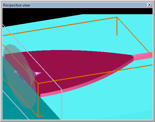
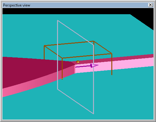
The left screenshot shows a waveguide input coupler. Suppose we want to use this system to excite a small gold nano-particle located at the end of the coupler (lower figure).
Example description
In the left figure, we see the entire coupler (facet, coupler, and output waveguide). The taper and waveguide are 500nm high. The coupler input width is 8.5 microns. The waveguide tapers over 10 microns to a width of 500nm, where it still supports many modes at wavelengths around 500nm. The dielectric waveguide is assumed to have an index of 2. The operating wavelength is 500 nm.
In the right figure, we see a 40 nm radius gold sphere, 200nm past the end of the taper region.
To simulate the entire device, the simulation region must be about 20x20x10 wavelengths in size. This is a large simulation. To accurately model the gold nano-particle, a very small mesh will be required (approx 5nm). Even with a graded mesh, this will still make the simulation substantially slower.
A more efficient solution is to break this simulation into 2 parts:
1) Model the large taper without the nano-particle using the normal mesh settings (mesh accuracy 2). A profile monitor is used to record the field profile at the taper output.
2) Model a nano-particle and a small portion of the taper. The field profile from the initial simulation will be used as the source field profile for the second simulation.
| Note: Reflection sensitive structure It is important to note this method assumes that there is not much reflection back from the Gold defect and that the waves recorded at the field monitor are not perturbed by the defect. This would not be a valid approximation in all simulations, therefore care must be taken when using this method to divide up a simulation into multiple simulations. |
Step 1: Model taper section. Record field profile at output
The simulation file usr_source_from_monitor1.fsp is used to model the taper section. In this file, the gold sphere has been removed (material properties set to air). A gaussian beam illuminates the facet. At the output of the taper section, a frequency profile monitor records the electric field at a wavelength of 500 nm.
The script usr_source_from_monitor1.lsf begins by running the simulation and plotting some initial results, as shown below. Next, it gets the E&H fields from the transmission monitor and packages them in a format that can be loaded into the Import source.
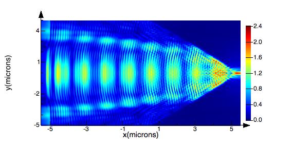 |E| in the taper | 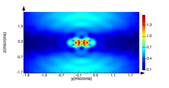 |E| field profile exported to the .fld file |
Step 2: Create custom source and simulate nano-particle
The script file then loads usr_source_from_monitor2.fsp, which contains the waveguide and gold sphere portion of the problem. The script loads the field data from the initial simulation into the Import source. After importing the field profile, you can open the source properties and see the field profile as shown below. You should see the same field profile that was recorded by the monitor in the last simulation.
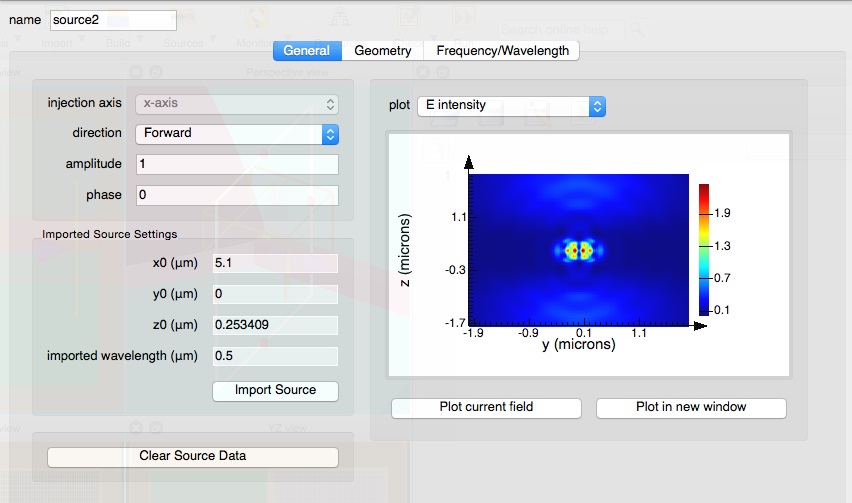
| Note: Data interpolation The field profile in the mat file is saved on the mesh of the first simulation. The mesh in the second simulation is different. In such situations, the field data will be automatically interpolated onto the new mesh. |
After running the second simulation, the script plots some initial results. First, the transmission and reflection in the waveguide after injecting the created source are shown. The reflection is effectively zero at 500nm, but increases slightly away from the wavelength where the field was recorded. This is because a physically correct waveguide mode profile will change as a function of frequency. However, we are injecting the mode profile that is correct at 500nm to be injected over a range of frequencies. Therefore, we expect some source injection error to result in reflection due to mode mismatch when running broadband simulations with this technique. If better accuracy is required, then a series of single frequency simulations will be required. The transmission is less than 1 because we are only measuring transmission in the waveguide region and are ignoring light that is propagating away into the air and substrate.
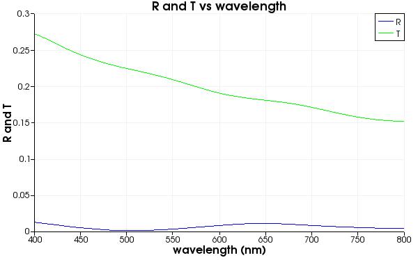
The second plot uses a box of 6 monitors surrounding the gold particle to calculate the absorption spectrum in the gold. This plot shows that there are 2 absorption resonances.
Using an equation to define the spatial field profile of a source in FDTD
 This topic explains how the Import source can be used to inject an arbitrary field profile into your simulation. In this example, the script can create an approximately radially polarized or azimuthally polarized beam.
Defining the field profile
Download the associated files. Open usr_custom_source.fsp and run the script file usr_custom_source.lsf. The script calculates the electric and magnetic fields at the source injection plane. The default settings in the script file will create a radially polarized beam, but you can modify the value of the "pol" variable in the script to specify an azimuthally polarized beam instead.
| Warning: The field profile calculated in this script is greatly simplified equation for a radial polarized beam that is intended for demonstration purpose only. |
Adding the source to your simulation
The script then packages the data into a dataset and loads that data into the Import source using the importdataset function. The data is also saved to a .mat file that can be later loaded into the Import source by editing its properties and pressing the "Import Source" button, as shown below.
Measure the profile with a monitor
As a final test, we can run the simulation and compare the field profile recorded by a monitor just in front of the source with the original EM dataset. After running the simulation, the script will plot both field profiles.


The measured field profile is very similar to what we originally specified.
The solver will attempt to inject whatever fields are specified, but it is important to recognize that specifying unphysical fields can lead to simulation errors. For example, there may be power normalization problems, source back reflections, or differences between the specified and actual injected fields.
| Note: Symmetric boundary conditions for custom field profiles Symmetry boundary conditions can be used whenever the EM fields have a plane of symmetry through the middle of the simulation region. For more information see Choosing between symmetric and anti-symmetric BCs |
Broadband Fixed Angle Source Technique (BFAST)
Broadband Fixed Angle Source Technique (BFAST) can be used when you have a periodic structure illuminated with a broadband source at an angle. It can provide broadband simulation results at a fixed angle of illumination.
When studying periodic systems, periodic Boundary Conditions (BC) allows you to calculate the response of the entire system by only simulating one unit cell, as mentioned in Periodic boundary conditions article. When a broadband plane wave is injected into a structure at an angle, special treatment will be required. One way is to use Bloch boundary condition. However, the actual injection angles for broadband illumination change with frequency, discussed in Plane waves - Angled injection. One way to solve this problem, the wavelength or frequency can be swept, or a number of incident angles are simulated and interpolation is required (see Bloch BCs in broadband sweeps over angle of incidence, for advanced users only). BFAST offers an alternate solution.
BFAST overview
A plane wave angled in xz plane (traveling along z axis) can be expressed as
→E(→r)=eikxx→E0
To remove the angular dependence from the field, a set of new variables is used, such as:
→Q(→r)=e−ikxx→E(→r)
and then the split field method (eg., split x component to xy and xz) is used to reformulate the FDTD update equations. Therefore, by reformulating the FDTD update equations, a new algorithm can be developed by removing this angle dependence. More details can be found in Liang's paper. Therefore, no Bloch BCs are required. It will have its own built-in boundaries conditions transverse to the propagation direction.
When to use BFAST
If you are simulating periodic structures with a broadband plane wave source illuminated at an angle, it might be worth trying BFAST. In this special formulation [1], the actual angle of injection does not change with frequency, making it significantly different from Bloch BCs. Furthermore it has been extended to ensure it is compatible with Lumerical's multi-coefficient material (MCM) models, and conformal mesh technology. Note, the BFAST technique may require special care for some cases to achieve stability. See the tips at the bottom of the page.
How to use BFAST
BFAST should ONLY be used with a single plane wave source. BFAST can be chosen in the General tab on the Edit plane wave source window, as shown in the image below to the left. Then users can set the incident angle and polarization angle. Other source parameters can be set as usual. As expected, all the wavelengths have the same injection angle, as shown in the image below to the right. In contrary, when Bloch BCs are used, the incident angles are a function of wavelength, as shown in the figure on angled broadband injection.
Once the "BFAST" is selected in the source, the Boundary Conditions transverse to the wave propagation are automatically overridden based on BFAST's formulation. For example if users choose "Bloch", "periodic", "Metal" or "PML" in the transverse directions, a warning sign will be shown. The figure below is showing a case when BFAST is chosen for a plane wave source injected along the z direction. In this case, the BCs in x and y directions should be overridden by the BFAST technique, shown by a warning sign to the right. However, the symmetry BCs can be reserved. Therefore, in this case, only the BCs in x direction are overridden by BFAST. PML is used in the z direction as usual.
If users set symmetric or anti-symmetric BCs, BFAST will keep and use them to save memory and speed up the simulation. For example, if the source is injected at an angle in xz plane but no angle in yz plane, yz plan can still use symmetry BCs fitting the source polarizations. In this way, users gain 2x simulation speed.
Along the direction of the wave propagation, users need to set the longitudinal BCs as "PML". For example, if the plane-wave injection plane is parallel to z axis, the transverse direction will be xz/yz planes, and the longitudinal direction is z. Usually zmin and z max use PML BCs.
As usual, the source injection plane should extend completely outside the simulation region, as shown in the figure below. Fortunately, the GUI can automatically do this for the users.
In some cases, users need to modify other BFAST parameters in FDTD "Advanced options". Under this tab, "BFAST" settings have two parameters:
- BFAST ALPHA: It is the smallest dielectric refractive index in the simulation region, and should generally be 1. For example, if the background index is set to 1.33 of water in FDTD "General" tab, then 1.33 should be used here instead of the default of 1.
- DT MULTIPLIER: It is used to further reduce the time step "dt" in "Mesh settings" in addition to the "dt factor". Its largest value is 1, meaning no change for the dt factor. When it is smaller than 1, the actual time step dt becomes smaller, in some cases it can overcome some diverging problems impossible by modifying other settings.
To summarize the usage of BFAST, the procedures are:
- set the "plane wave type" as "BFAST" in the Source General tab
- set the Boundary conditions along the longitudinal direction as PML. GUI will automatically use BFAST's built-in boundary conditions in the transverse directions. For consistency, user may set "Bloch" in the plane of angle incidence (though it is overridden), and symmetry BCs in no angle plane if applicable.
- occasionally some advanced settings need to be modified.
Example
Below is an example of dielectric stack with angled illumination at 60 degree (polarization angle 90) of a 2D simulation, and comparison to theoretical result. To duplicate the results, you can download and run best_stack.fsp.
More examples can be found in the Knowledge Base.
Angle sweep
In some cases users need to get results of broadband incidence at different incident angles. This can be done by use of sweep as usual to sweep the incident angle. Different from Bloch BC case, in BFAST, at each specified incident angle, all the wavelengths have the same angle, so no further interpolation is required. In this example, the incident angle is set inside "model", so when the incident angle is set in sweep, the correct quantity must be chosen. To get sweep result, open the bfast_stack.lsf and set sweep=1 and run the sweep, the following images of reflection and transmission are shown below:
Reflection, Transmission
BFAST FDTD is fundamentally different from the standard FDTD formulation because the core update equations are changed, in addition to the boundary conditions. As a result, there are some limitations:
Limitations
- The time step, dt, must be reduced compared to standard FDTD as the angle of incidence increases in order to preserve numerical stability (see the next section). This is controlled by the "dt multiplier". As a result, steep angle simulations will take more time to run. For this reason, it is important to consider if BFAST is the right method for your application. If your bandwidth is small, or your angle of incidence is small, you may get faster results by using Bloch boundaries conditions. Certainly, if you are only looking for results at a single wavelength, you should use Bloch boundary conditions. The simulation time ratio for BFAST relative to a regular FDTD simulation.
| Angle (degrees) | 0 | 10 | 20 | 30 | 40 | 50 | 60 | 70 | 80 |
| Simulation time | 1.0x | 1.2x | 1.5x | 2.0x | 2.8x | 4.3x | 7.5x | 16.6x | 65.8x |
-
BFAST is best suited to non-dispersive dielectric materials and materials with high loss such as metals. Low loss materials, including silicon and other semiconductors, may cause the simulation to diverge due to gain in the numerical permittivity. Use the sample code in getnumericalpermittivity, with the use_BFAST=1, to see the numerical permittivity.
- Nonlinear materials are not compatible with this method. As a result, nonlinear and all flexible material plugin materials will not function using BFAST in current version.
- Injection above the critical angles for total internal reflection (TIR) is not allowed. There is no possible stable time step dt in this case. For example, injecting light at 50 degrees in glass that is incident on a glass/air interface is not stable. However, if you are injecting light in a lower index medium onto a higher index medium, then it is allowed. For example, if you are injecting light from glass onto a higher index substrate, such as silicon, then you can use BFAST - however, the value of "bfast alpha" should be set equal to the smallest refractive index used anywhere in your simulation.
The software can automatically detect if there is total reflection for the source injection. A warning message will be shown as below:
If you see this warning message, you can use the Bloch+plane wave method with frequency sweep.
Numerical stability
BFAST is more numerically unstable than standard FDTD. There are several sources of instability and most problems can be solved by adjusting certain settings. If you encounter any problems that cannot be easily solved, please contact us for assistance. Most problems and their solutions are listed here:
- The PML can be unstable for long duration simulations. If it becomes unstable, we recommend increasing the number of layers and reducing the value of pml sigma. Sometimes the "steep angle PML" may work better.
- Dispersive media can become unstable much more easily. These problems can sometimes be fixed by reducing the "dt multiplier" until stability is achieved.
- Dispersive media with low loss (eg. semiconductors) can be unstable due to gain in the numerical permittivity. This can sometimes be avoided by experimenting with the material fitting parameters (tolerance, max coefficients, improve stability, make fit passive, bandwidth). Use the sample code in getnumericalpermittivity, with the use_BFAST=1, to see the numerical permittivity.
- When using dispersive media, the numerical stability is greatly increased by using a uniform mesh over the dispersive materials in the direction transverse to the source injection axis. For example, when considering the scattering of a gold particle on a surface, as shown below for a 2D simulation, a mesh override region that extends at least 1*dx outside of the gold region should be used. This mesh override region should force a uniform mesh in dx – but does not have to force a uniform mesh in dy. The figure below summarizes these settings. Note that practically, we would often also force a uniform dy mesh to achieve accurate results for this plasmonic structure. Furthermore, it is often simple to use a uniform value of dx across the entire unit cell but this is not necessary for numerical stability.
Summary and Tips
Setting to use BFAST is relatively easy, as described above. However, due to its special formulation, simulation time for a single project file may be a little longer than expected. In addition, at larger angles, simulation speed is further decreased, and the accuracy can be degraded. There is always a compromise in simulation between the simulation time spent and the accuracy obtained. Users are advised to make some tests to choose whether BFAST is the most in favored method for the cases at some steep angles or with very strong dispersive materials. In addition, converging test may give you confidence for the accuracy it can reach.
- BFAST: Always check "BFAST" in the "plane wave type" at the source if you want to simulate angled-broadband source using BFAST; this ensures that all the wavelengths will have exactly the same incident angle.
- dt multiplier: The default dt multiplier of 0.5 is chosen for most cases. However, to speed up the simulation, users can increase it up to 1 (eg., for pure dielectric without dispersion) if simulation does not diverge.
- dt multiplier: For strongly dispersive materials, smaller dt multiplier may be required to have stable simulation.
- mesh: Users may use a little higher mesh accuracy than usual (2 by default);
- mesh: Uniform mesh is recommended in the transverse directions.
- mesh: if strong dispersive material is involved, override region should be larger than the structure as shown above.
- accuracy: Better accuracy can be achieved even at larger incident angles if the materials involved in the simulation are dielectric without dispersion.
- accuracy: The accuracy may degrade when the indent angle is large. You may need to test the results by use of the Bloch BCs to see if you are satisfied with the accuracy.
- speed up: Usual symmetry BCs can be used if the source has zero incident angle in that plane;
- speed up: if the smallest refractive index (constant dielectric material, including the background) in the simulation is not 1, set "bfast alpha" to the smallest dielectric refractive index;
- PML: If relatively large incident angle is simulated, you may choose "steep angle" PML;
- PML: along the axis of source injection, PML BCs are used. When higher mesh accuracy is used, users may need more number of PML layers from default setting.
- BCs: in the transverse plane, the BCs in the plane of angled incidence are automatically overridden for whatever the previous BCs are set. However, in the plane of no angle, the symmetry BCs are conserved.
- critical angle: Currently it will not support the case where the incident angle is very close to and larger than the critical angle. This can happen when the source is located at higher index material than that in the rest of the simulation region.
Related publications
[1] B. Liang et al, Wideband Analysis of Periodic Structures at Oblique Incidence by Material Independent FDTD Algorithm, IEEE Trans. Antennas & Propagation, Vol.62 ,No.1, PP. 354 - 360.
Understanding coherence in FDTD simulations
 FDTD is a fundamentally coherent simulation method. Below, we discuss three types of incoherence that are relevant for FDTD simulations, and the difficulties in direct simulation of these effects. In many physical processes, we have a combination of all types of incoherence.
The following sections provide three examples that show how to model various incoherent effects with FDTD and MODE' propagator.
Temporal phase incoherence
The phase, j, of the light shifts randomly over time, on a time scale tc. For light near visible wavelengths, we have
→E(t)=→E0cos(ωt+φ(t))
T=2πω≈10−15S
τc≈10−11s
It is not practical to simulate the statistics of temporal phase incoherence because tc >> T.
Spatial incoherence
A spatially incoherent source could be, for example, an ensemble of dipole emitters spread over a given volume. Each dipole is independent of its neighbors, and emits radiation with a random phase that varies on a time scale on the order of tc. At any given instant, the relative phases of all the dipoles are fixed, however, on a time scale of tc the relative phases of the dipoles change in a completely random fashion. The direct simulation of spatial incoherence requires simulations for very long periods of time or a large amount of ensemble averaging with one FDTD simulation per ensemble. Therefore it is not practical to simulate spatial incoherence directly in most cases.
Polarization incoherence
In a similar manner to temporal phase incoherence, the polarization of a beam or the orientation of a dipole source depends on time. In the case of an unpolarized beam we have
→E(t)=→u(t)E0cos(ωt)
where the unit vector u(t) defines the beam polarization and varies on a time scale tc >> T. In the case of a dipole source, we have
→p(t)=→u(t)p0cos(ωt)
where the unit vector u(t) defines the dipole source polarization and varies on a time scale tc >> T.
In both cases, the time scale for the variation of the polarization is much larger then the optical cycle, making it unpractical to simulate the statistics of temporal polarization incoherence with FDTD.
How to simulate incoherent phenomena with FDTD
Direct simulation of incoherent effects requires simulations that last many times the correlation time (tc) which is typically many orders of magnitude larger than the optical cycle. In some cases, ensemble averaging can be used but this requires a very large number of simulations. Therefore to simulate the physical conditions required for incoherence means simulation times that are far too long to be practical in most cases.
In general, a more efficient approach is to calculate the statistical averaging analytically rather than performing lengthy or numerous simulations. In general, this requires a small number of simulations and some post-processing of the data. In the following sections, we explain how to perform this post-processing in a number of examples that can be applied to most simulations of incoherent processes.
Understanding temporal incoherence in FDTD
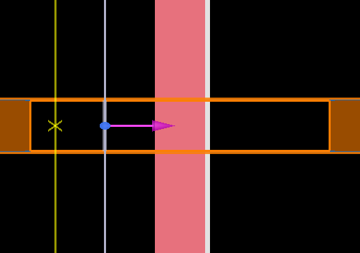 This page goes over the problems associated with direct simulation of temporal incoherence, the recommended simulation method, and provides an example simulation.
Problems with direct simulation
The phase, φ, of the light shifts randomly over time, on a time scale τc. For light near visible wavelengths, we have
→E(t)=→E0cos(ωt+φ(t))
T=2πω≈10−15S
τc≈10−11s
Even without random phase shifts, if the light is not monochromatic, it is incoherent.
In either case, the coherence length of the system is often much longer than any standard simulation time (τc>>T), so it is not efficient in general to directly model temporal incoherence. It is not possible to perform near to far field projections of incoherent results in the near field.
Recommended simulation method
By default, the frequency domain (DFT) monitors of FDTD return the monochromatic response of the system.
There are some advanced features to directly extract incoherent results (ie. where the value of Δf ~ 1/τc can be specified) - see Spectral averaging for more detail.
In general, the best approach is to calculate the monochromatic (or CW) response first, then calculate the incoherent result with
〈∣∣→E(ω0)∣∣2〉=∫W(ω)|→E(ω)|2dω
where W(w)
is the spectrum of the physical source used.
Temporal Incoherence Example
In usr_temporal_incoherence.fsp, we simulate the reflection from a 50 nm film of silver on a 500 nm slab of silicon. The associated script file, usr_temporal_incoherence.lsf uses the monochromatic results from the simulation to calculate the incoherent results (between 500 and 700 nm) for coherence lengths of 15 um and 300 um for a physical source with a Lorentz function spectrum. The resulting plots are shown below.
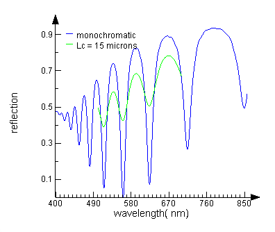 | 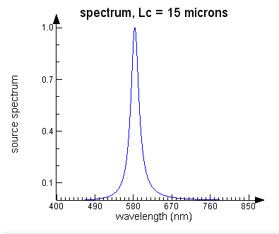 |
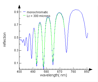 | 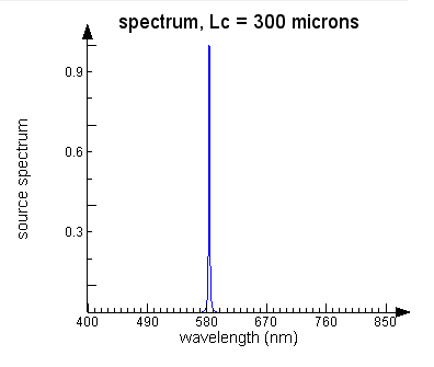 |
Changing the source bandwidth in FDTD and MODE
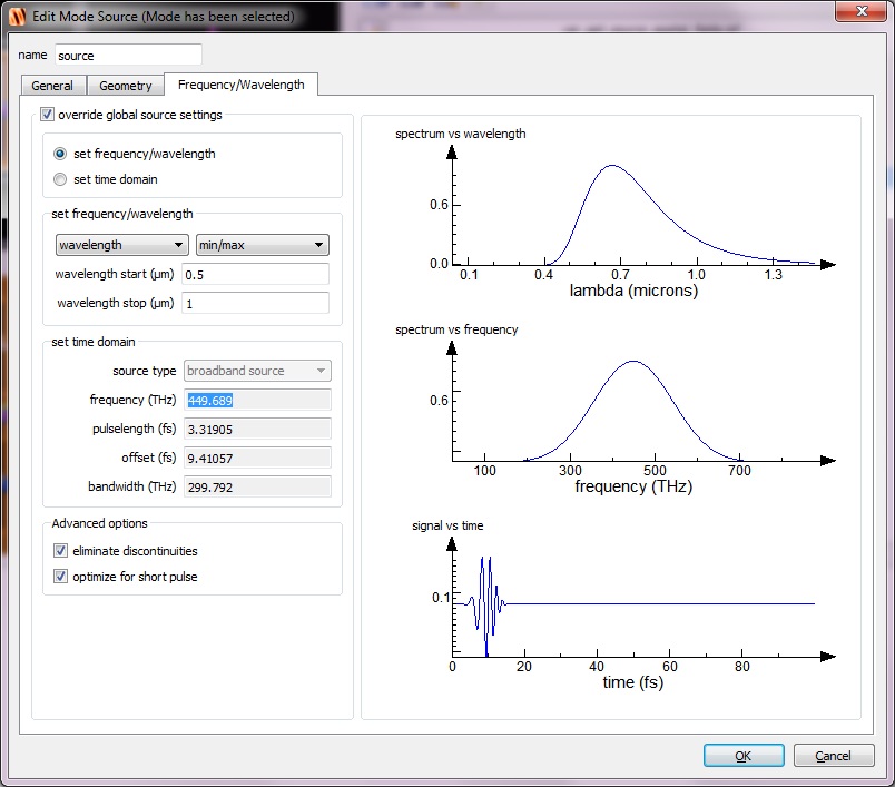 This page discusses how to control the bandwidth of the source pulse.
By default, FDTD and MODE automatically calculate the source pulse shape and bandwith from the Start & Stop wavelength values specified by the user. A pulse is used EVEN when you want steady state, CW results at a single frequency.
In FDTD, the 'Optimize for short pulse' option is enabled by default, meaning that a very short pulse is typically used. In MODE, this option is disabled by default, leading to a slightly longer pulse (although still quite short).
Optimize for short pulse: enabled
This is the default setting for FDTD, meaning a very short pulse will be used in most simulations.

Optimize for short pulse: disabled
This is the default setting for MODE, meaning a slightly longe pulse will be used in most simulations. Using a slightly longer pulse minimizes the amount of power injected at frequencies outside the range of interest, minimizing numerical stability problems.
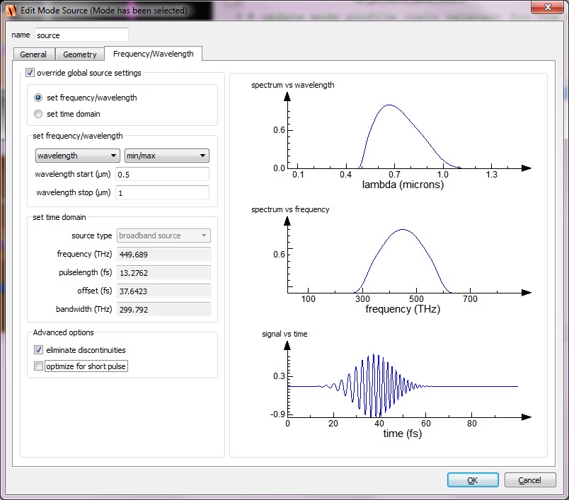
For the majority of simulations, the default source pulse settings work well. However, in some special situations, you may need to modify the source pulse settings:
Very wide band pulse (ex. searching for resonant modes)
When studying resonators, the first task is generally to determine the resonant frequencies. A very wide band source can be used to determine all resonant frequencies from a single simulation. Typically the frequency range of interest is 0->fmax. This type of source is easily generated with the Set Frequency frame of the Frequency / Wavelength tab. Set the frequency start value to a small value(zero is not allowed). Set frequency stop to fmax.
In the following example, the source range is 1-601 THz. Notice the broad spectrum in the Spectrum vs frequency plot, and the very short source pulse in the Signal vs time plot.
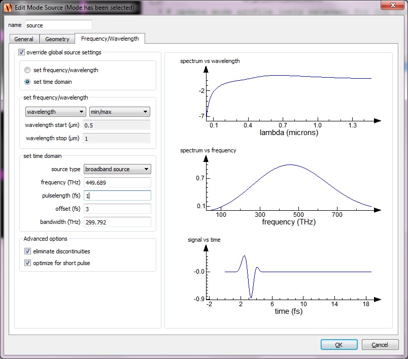
Narrow band source (ex. some non-linear simulations, some divergence problems, etc)
In some some situations, it is necessary to create pulse with a narrow bandwidth, or to minimize the amount of power that is injected outside the specified wavelength range. In such cases, you can disabled the 'Optimize for short pulse' option. If that is not sufficient, you can select the 'set time domain' option and increase the Pulse length and Offset properties as much as needed. If these settings are increases significantly, you may need to increase the overall simulation time.

| NOTE: The 'eliminate dc' option can be used to eliminate the DC component of the source signal by forcing a symmetry on it. Enabling this option grays out the rest of the "Advanced options" - 'eliminate discontinuities' and 'optimize for short pulse'.
|
Creating a custom source time signal for an FDTD source
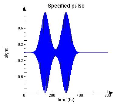 This topic explains how to create a custom time signal for a source. In this example, we create a signal with two gaussian shaped pulses. It's worth noting that creating a custom time signal is rarely required. If you are looking to simply modify the source bandwidth (ie. to create a longer, more narrow band pulse), see Changing the source bandwidth. For linear time-invariant systems, it is possible to use the impulse analysis to determine the response to an arbitrary time signal.
To create a custom source time signal, the setsourcesignal function requires a complex valued function. However, we typically only have a real valued signal. The script usr_custom_time_signal.lsf show how to convert a real valued function into a complex valued function using an fft.
The first part of the script shows how to define a real valued time signal. In this example, we simply use a sine wave with a dual-gaussian envelope. Next, the script shows how to convert a real valued signal into a complex valued signal. After that, the custom time signal is loaded into the source. Finally, we run a simulation and compare the specified pulse with the actual simulation results.
To reproduce the following figure, open the simulation file, then run the script.
|
This figure shows the Specified signal, the actual Source signal used in the simulation, and the resulting field profile as measured by a time monitor. |
This is a zoomed in version of the same figure. We can see that the Specified signal and Source signal are very similar. The Signal from the time monitor is delayed by about 1/4 wavelength, as expected due to the spatial offset between the source and monitor. |
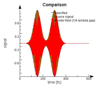
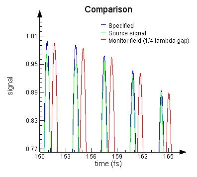
| Note: Custom source time signals and spectra Customizing the source time signal or spectrum is an advanced feature. In the vast majority of simulations, it is best to simply specify the frequency/wavelength range of interest and let the software calculate the best source time signal. It is usually far easier and more efficient to model a particular source time signal or spectrum (ie. the solar spectrum) during data post processing. For more information, see Using the impulse response to calculate the systems response to an arbitrary input or the Solar source spectrum page. Non-linear simulations are the one application area where custom time signals may be necessary. |
| Note: Auto shutoff and time signal length By default, the auto shutoff function does not kick in until the specified time signal length is done. So one would see auto shutoff value stays at 1 even though the amount of remaining field is actually small in the simulation. For example, for the above custom time signal, the auto shutoff does not start to function until 600 fs (the time length specified in the script file), although the pulse is physically done at around 400 fs. In order to have the auto shutoff working ASAP, user should specify a minimum time length possible, say, 450 fs for this source. |
Creating a custom source spectrum for an FDTD source
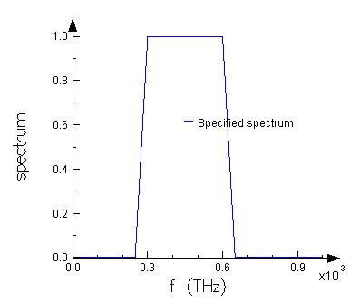 This topic explains how to create a custom source spectrum. First, we must design a time signal with the desired spectrum. Next, we set the source to use this custom time signal with the setsourcesignal function. Finally, we confirm the spectrum with a time monitor.
| Note: Custom source time signals and spectrums Customizing the source time signal or spectrum is an advanced feature. In the vast majority of simulations, it is best to simply specify the frequency/wavelength range of interest and let the software calculate the best source time signal. It is usually far easier and more efficient to model a particular source time signal or spectrum (ie. the solar spectrum) during data post processing. For more information, see Using the impulse response to calculate the systems response to an arbitrary input or the Solar source spectrum page. Non-linear simulations are the one application area where custom time signals may be necessary. Before implementing a custom source time signal or spectrum, we strongly recommend visiting the Support Center to discuss your needs. |
Use usr_custom_spectrum.lsf to create a source with a specified power spectrum.
Setup source
 | Specify the desired spectral shape in the first section of the script file. In this example, we specify a sloped-wall top-hat function. |
 | The time signal length must be specified in the Setup section of the script file. In this example, the source length is 30 fs. This figure shows the time signal we have calculated. |
 | The figure on the left shows the specified spectrum, and the actual spectrum that we expect, based on the above time signal. Notice they are not identical. The calculated spectrum will converge to the specified spectrum as the time signal length is increased. |
Test source in FDTD simulation
The final section of the script file loads the time signal into the source and runs a simple simulation. We can calculate the actual spectrum of the source in the FDTD simulation with the sourcepower function. It would also be possible to confirm the spectrum with a time monitor, if there are no structures in the simulation. Structures in the simulation will create reflections that will interfere with the source pulse. This interference would alter the spectrum that the time monitor measures.
 | This figure shows the actual time signal used by the source in the FDTD simulation. Notice the phase offset as compared to the calculated time signal. By adjusting the source phase setting, the phase of the fdtd time signal could be matched to the calculated signal. |
 | This figure shows the actual source spectrum obtained with the sourcepower function. Once again, the spectrum is similar to the Specified and Expected spectrums, but slightly different. The difference between the FDTD and the calculated spectrum occurs because the fdtd simulation uses a larger dt than the calculated spectrum. |
Monitors
Refractive index monitor - Simulation object
![]()
Index monitors records the n and k value as a function of frequency/wavelength in a simulation. In the future, the index monitor will be able to capture the time-evolution of the physical properties profile for nonlinear media.
In FDTD, it is possible to preview the index profile while still in Layout mode (i.e. without running the simulation). Note that the index preview returns a slightly simplified version of what the index monitor provides after running the simulation. Some advanced settings (such as the spatial interpolation setting) will be ignored in the preview.
| Notes : Memory and computation time Index monitors generally have modest memory requirements. To minimize the amount of memory required, use 1D or 2D rather than 3D monitors. Similarly, try to minimize the number of frequency points recorded. By default, only one frequency point is recorded. It is also possible to use spatial downsampling to record less spatial resolution. Generally, Index monitors don't have a large effect on the simulation time, except when recording a very large amount of data. All the index monitor data is calculated at the beginning of the simulation. |
General tab
Simulation type: Record the type of simulation data, default setting is ALL
Override global monitor settings:
A toggle to override the global monitor settings. If checked, users can specify the frequency range and number of points at which frequency-domain information will be recorded (using the options described below). If unchecked the options below are set from the global monitor settings.
SAMPLE SPACING: This combo-choice parameter determines how the sample frequency/wavelength will be selected. The three sample options are "uniform", "chebyshev" and "custom".
- USE WAVELENGTH SPACING: By default, data is recorded at certain spaced points with respect to frequency. Selecting this option spaces data at certain spaced points with respect to wavelength.
- USE SOURCE LIMITS: When checked these monitors use the source limits. When unchecked, the frequencies/wavelengths at which to record data can be set using the pull down menus and boxes below them.
- FREQUENCY POINTS: Set to choose the number of frequency points at which to record data.
When sample spacing is selected to be "custom", all the above settings will be disabled and a "custom frequency samples" table will be shown. Properties of the table are:
- ADD: Adds an entry above the selected entry to the "frequency (THz)" table
- REMOVE: Removes the selected entry from the "frequency (THz)" table
- SORT: Sorts the table with frequency from low to high
- set global monitor settings: Access to global properties
Geometry tab
Monitor type: The monitor type and orientation, this option will control the availablity of spatial settings below
- X, Y, Z: The center position of the simulation region
- X MIN, X MAX: X min, X max position
- Y MIN, Y MAX: Y min, Y max position
- Z MIN, Z MAX: Z min, Z max position
- X SPAN, Y SPAN, Z SPAN: X, Y, Z span of the simulation region
The DOWN SAMPLE X, Y, Z option is used to set the spatial downsampling performed by the monitor. A down sample value of N corresponds to sampling (recording) the data every Nth grid points. Setting the down sample value to 1 gives the most detailed spatial information (i.e. information at each grid point).
Advanced tab
| WARNING: This tab includes options which should only be changed if you are quite familiar with the meshing algorithm and techniques used. |
- SPATIAL INTERPOLATION: In FDTD generally, the electromagnetic field components and material properties are not known at the same point in space. Instead each component of the vectorial electric and magnetic fields are recorded at different locations in the Yee cell. Therefore, the material properties are also known at various locations within the Yee cell. This setting controls how the index monitor calculates the refractive index data. The SPECIFIED POSITION (Default) returns the index data where the monitor is located. This type of data is convenient for many purposes, but it is important to remember that the actual FDTD engine calculates the fields at locations other than the Yee cell origin. The NEAREST MESH CELL option is very similar, but the monitor location is snapped to the nearest mesh cell. The NONE option records the index data at the locations actually used by the FDTD engine.
| Note: Spatial interpolation - NONE setting Disabling the spatial interpolation is a very advanced feature. Only expert users who are very familiar with the FDTD method should consider using this feature. Most standard analysis functions (such as the transmission script function, the data visualizer, etc) assume that the spatial interpolation is enabled. They may not give the most accurate result when used to analyze such monitor data. All analysis must be done manually. |
- RECORD DATA WITHIN PML: This option is as described above for time domain monitors.
- RECORD CONFORMAL MESH WHEN POSSIBLE: Enabled by default. The index monitor will record the the effect of the conformal mesh. It is helpful to disable this option when doing absorption calculations. The conformal mesh information can only be recorded when using the 'NEAREST MESH CELL' or 'NONE' spatial interpolation setting, and when the spatial downsampling option is set to 1.
- RECORD SURFACE CONDUCTIVITY: The index monitor will record the surface conductivity which is used in the simulation and return this as the SURFACE CONDUCTIVITY result. This may be used if you want to record the surface conductivity components over space when using SPECIFIED POSITION, or NONE as the spatial interpolation option.
Results returned
The results that index monitors return depends on the modes the simulation is in.
In ANALYSIS mode:
- INDEX: Refractive index as a function of position and frequency/wavelength.
- INDEX_DETAIL: A matrix dataset with parameters x,y,z,f. This is a result when the "spatial interpolation" is set to "none". It also contains duplicate parameter entries for x,y,z called x_offset, y_offset and z_offset, respectively. These are the positions offset in the Yee cell. To obtain data at the correct spatial locations for index_x, you should use parameters (x_offset,y,z,f), for index_y you should use parameters (x,y_offset,z,f) and for index_z you should use (x,y,z_offset,f). This is useful in the script and can also be done in the visualizer. This type of capability would make absorption calculations like this example easier. For further information about why different positions in the Yee cell are used for each field component, please refer to the FDTD Solver Physics page.
- SURFACE CONDUCTIVITY: This will return the same result as the surface conductivity preview by default. If the RECORD SURFACE CONDUCTIVITY option under the ADVANCED TAB is enabled, this will instead return the surface conductivity used in the simulation which will include the effect of the selected spatial interpolation option.
In LAYOUT mode:
In addition to the "index preview" result, the index monitors have "index" results and (when spatial interpolation is set to None) "index_detail" results. All of these 3 results require meshing in the UI when the user asks for the results and therefore could trigger a big calculation, especially for large 3D index monitors. The difference is:
- "index preview" does not try to keep track of conformal meshing or any yee grid offsets. It is therefore the fastest and useful to ensure that the structure is basically correct.
- "index" and "index_detail" are guaranteed to give exactly the same results that you will get in ANALAYSIS mode, as if the simulation had been run. This can be slower if, for example, you are recording conformal mesh properties.
- INDEX PREVIEW: Refractive index as a function of position and frequency/wavelength before the simulation runs. It is important to note that the preview data is not exactly the same as the data returned after the simulation runs. Some advanced settings, such as spatial interpolation options and conformal meshing are ignored when calculating the index preview.
- INDEX: Refractive index as a function of position and frequency/wavelength. Same as in ANALYSIS mode.
- INDEX_DETAIL: Refractive index dataset including the positions offset parameters. Same as in ANALYSIS mode.
- SURFACE CONDUCTIVITY PREVIEW: Surface conductivity as a function of position and frequency/wavelength before the simulation runs. This is useful tool to make sure the graphene object is positioned as desired.
Field time monitor - Simulation object
![]()
These monitors provide time-domain information for field components over the course of the simulation. Time-domain monitors can consist of point, line, or area monitors to capture this information over different spatial extents within the FDTD and varFDTD simulation regions. For the purposes of extracting line widths of resonant structures through Fourier analysis, point time monitors with a down sample time of 1 are sufficient.
Memory and computational requirements: Generally, time monitors don't have a large effect on the simulation time. However, they can require large amounts of memory when recording data over a large spatial domain. When possible, use 1D rather than 2D or 3D monitors. Similarly, you can reduce the duration of time where data is recorded. Temporal down sampling is also used to minimize the amount of data collected. Finally, it is possible to control which field components are recorded on the Data to record tab.
General tab
The general tab for the time domain monitor includes options to edit the amount of data, and time period over which data is collected.
- Simulation type: Record the type of simulation data, default setting is ALL
- Stop method: End of simulation, Choose stop time, choose number of snapshots
- Start time: The time to start recording
- Stop time: The time to stop recording, choose stop time option
- Number of snapshots: the number of time step to record, related to the dt setting in mesh settings tab
Geometry tab
Monitor type: The monitor type and orientation, this option will control the available of spatial setting below
- X, Y, Z: The center position of the simulation region
- X MIN, X MAX: X min, X max position
- Y MIN, Y MAX: Y min, Y max position
- Z MIN, Z MAX: Z min, Z max position
- X SPAN, Y SPAN, Z SPAN: X, Y, Z span of the simulation region
The DOWN SAMPLE X, Y, Z option is used to set the spatial downsampling performed by the monitor. A down sample value of N corresponds to sampling (recording) the data every Nth grid points. Setting the down sample value to 1 gives the most detailed spatial information (i.e. information at each grid point).
Data to record
- OUTPUT Ex, Ey, Ez, Hx, Hy, Hz, Px, Py, Pz: A set of fields with which the user can select what field components (Ex, Ey, Ez, Hx, Hy, Hz) or Poynting vector (Px, Py, Pz) to measure. In 2D simulations, only some components are non-zero (i.e. only Ex, Ey, and Hz are applicable for TE simulations). All the field quantities remain active to facilitate easy change between TE and TM simulations.
- OUTPUT POWER: For surface monitors (3D) and line monitors (2D) only. You can calculate the integrated power over the monitor surface. This requires much less memory after the simulation is completed and is particularly suitable for large parallel simulations where only the integrated power across a surface is required.
- PLUGIN MATERIAL: For point monitors only. When a plugin material is used in a simulation, the time monitor can return the storage fields if the material is chosen. Note: the point monitor has to be placed in the object that uses this plugin material in order to return meaningful storage fields.
Advanced tab
| WARNING: This tab includes options which should only be changed if you are quite familiar with the meshing algorithm and techniques used. |
- SPATIAL INTERPOLATION: In FDTD generally, the electromagnetic field components are not recorded at the same point in space. Instead each component of the vectorial electric and magnetic fields are recorded at different locations in the Yee cell. In order to properly calculate the Poynting vector and electromagnetic energy density, the fields are interpolated to the same location in the Yee cell. This setting controls how the fields are interpolated. The options for time monitors are NEAREST MESH CELL (Default) and NONE. With NEAREST MESH CELL, the fields are interpolated to the nearest FDTD mesh cell boundary. With NONE, no interpolation is performed and each electromagnetic field component is recorded at a different position within the Yee cell.
| Note: Spatial interpolation - NONE setting Disabling the spatial interpolation is a very advanced feature. Only expert users that are very familiar with the FDTD method should consider using this feature. Most standard analysis functions (such as the transmission script function, the data visualizer, etc) assume that the spatial interpolation is enabled. They may not give the most accurate result when used to analyze such monitor data. All analysis must be done manually. |
- RECORD DATA WITHIN PML: Collect monitor data within the PML boundary condition region. This is a very advanced option that should rarely be used. Contact Lumerical support before enabling this option. The simulation region - EXTEND STRUCTURE THROUGH PML option must be disabled when using this option.
- MIN SAMPLING PER CYCLE: This parameter determines the minimum amount of sampling per optical cycle that can be used. By default, it is set at 10.
- SAMPLING RATE: The actual sampling rate in Hz.
- DOWN SAMPLE TIME: This is the time step downsampling.
| Note: Sampling Rate When calculating the spectrum the frequency resolution is equal to the size of the FFT window divided by the sampling rate. FDTD will use zero-padding so the spacing between frequency points is N\SAMPLING RATE where N=2^13. Min and max resolvable frequencies are:
|
- Min: Sampling Window - fs/N
|
If the impulse has not decayed before the end of the simulation the FFT is invalid. One should not increase the sampling rate above 1/dt where dt is the FDTD timestep. For more information see fft - Script command, or czt - Script command. |
Results returned
Results
- E: Electric field data as a function of position and time.
- H: Magnetic field data as a function of position and time.
- P: Poynting vector as a function of position and time.
- SPECTRUM: The fourier transform of the electric and magnetic fields as a function of position and frequency/wavelength. (point monitor only)
- RESONANCES: Returns frequency, decay constant, Q-factor, amplitude and phase of resonances. For more information, see findresonances. (point monitor only)
| Note: Manual calculation of SPECTRUM result The following code can be used to manually calculate the spectrum data (eg. if it is necessary to adjust the frequency range of the data). # this code can be used to manually calculate the
# spectrum result from time monitor data
# get E/H time domain fields
E = getresult("monitor","E");
H = getresult("monitor","H");
# user can specify frequency range of interest
f = linspace(50e12,1000e12,10000);
# calculate czt of time domain data
Exw = czt(pinch(E.Ex),E.t,2*pi*f);
Eyw = czt(pinch(E.Ey),E.t,2*pi*f);
Ezw = czt(pinch(E.Ez),E.t,2*pi*f);
Hxw = czt(pinch(H.Hx),H.t,2*pi*f);
Hyw = czt(pinch(H.Hy),H.t,2*pi*f);
Hzw = czt(pinch(H.Hz),H.t,2*pi*f);
# package results into a dataset
spectrum = rectilineardataset("spectrum",E.x,E.y,E.z);
spectrum.addparameter("lambda",c/f,"f",f);
spectrum.addattribute("E",Exw,Eyw,Ezw);
spectrum.addattribute("H",Hxw,Hyw,Hzw);
# visualize dataset
visualize(spectrum); |
| Note: Plugin material - storage fields For point monitors inside an object that uses a plugin material, the data in the storage fields can be found in the rawdata returned by the monitor (see below). |
Raw data
- POWER: Instantaneous power as a function of time. This data is only returned when surface monitor (3D simulation) or line monitor (2D simulation) is used, with the "output power" option checked in the Data to record tab. For more information or an example using this data, see Parseval's theorem.
- STORAGE_FIELDS: Only for plugin materials. Extra data is available if the storage field is properly specified in the .cpp file when the material is complied. The software automatically chooses the x,y,z-direction where the fields are meaningful to show. For more information, see plugin material.
Movie monitor - Simulation object
![]()
Movie monitors capture a desired field component over the region spanned by the monitor for the duration of the simulation. Movie monitors are only available in the two-dimensional variety (and only z-normal for propagator simulations). The resultant movies are saved with the same name as the monitor in the current working directory.
| Tip: Computations requirements Memory: Movie domain field monitors usually require modest amounts of memory. To reduce the memory requirements, reduce the output movie resolution. Computation time: Movie monitors can have a large effect on the simulation time. Consider disabling your movie monitors to increase the simulation speed. |
Note: It is possible to create a CW movie from profile or power monitor data.
General tab
Simulation type: Record the type of simulation data, the default setting is ALL
- HORIZONTAL RESOLUTION: The horizontal width of the final movie, in pixels.
- VERTICAL RESOLUTION: The vertical height of the final movie, in pixels.
- SCALE: A dimensionless variable that defines how to scale the capture of the field data, with the tendency that a scale factor too small will result in saturation of the movie, while a scale factor too large will result in very faint radiation patterns. This parameter may not be less than zero. Once the simulation is run, the monitor outputs its maximum intensity at the end of the simulation in the variable "maxI". Setting the scale factor to the value of "maxI" and rerunning the simulation will result in a perfectly scaled movie.
- DRAW STRUCTURE OUTLINE: A toggle that allows the user to superimpose an outline of the refractive index profile on top of the movie. This can be used to aid in visualization of where the radiation is located within the dielectric structure.
- TM, TE FIELD COMPONENT: 2D simulations. The field component to be captured in the movie. The choices depend on whether a TE or TM simulation is being performed, as set out in the FDTD simulation region. If a TM simulation is being performed, the TM field component is captured to the movie, whereas if a TE simulation is being performed, the TE field component is captured. Can also be ELECTRIC FIELD INTENSITY (|E|2) or MAGNETIC FIELD INTENSITY (|H|2).
- FIELD COMPONENT: 3D simulations. The field component to be captured in the movie. Can also be ELECTRIC FIELD INTENSITY (|E|2) or MAGNETIC FIELD INTENSITY (|H|2).
Geometry tab
Monitor type: The monitor type and orientation, this option will control the available of spatial setting below
- X, Y, Z: The center position of the simulation region
- X MIN, X MAX: X min, X max position
- Y MIN, Y MAX: Y min, Y max position
- Z MIN, Z MAX: Z min, Z max position
- X SPAN, Y SPAN, Z SPAN: X, Y, Z span of the simulation region
Advanced tab
Note: This tab includes options that should only be changed if you are quite familiar with the meshing algorithm and techniques used.
- MIN SAMPLING PER CYCLE: This parameter determines the desired amount of sampling per optical cycle.
- SAMPLING RATE: This converts the minimum points per optical cycle into an actual sampling rate in Hz.
- DOWN SAMPLE TIME: This is the time step downsampling.
- FRAME RATE: The speed at which frames are displayed on the screen, in units of frames per second. The default is 30.
- RECORD DATA WITHIN PML: This option is as described above for time-domain monitors.
Results returned
- A movie file (.mpg) named after the simulation file name is generated. The file can be found in the same directory as the simulation file. To view the movie, use a 3rd party movie player such as Windows Media Player.
Frequency-domain Profile and Power monitor - Simulation object
![]()
![]()
Frequency-domain field monitors collect the field profile in the frequency domain from simulation results across some spatial region within the simulation in the FDTD, varFDTD solvers.
Note: There are two very similar types of frequency domain field monitors: 'Frequency domain field profile' and 'Frequency domain field and power' monitors. These monitors are identical except for one advanced setting (the spatial interpolation setting). In most situations, we recommend using the 'field and power' monitor. This monitor 'snaps' to the nearest mesh cell, which minimizes the amount of interpolation required, generally leading to more accurate data. The 'profile' monitor does not snap to the nearest mesh cell. Instead, it records the data exactly where the monitor was located. This can be useful in a few situations, but the extra interpolation required can slightly reduce the accuracy of the data.
| Tips: Memory and computation time Frequency domain field monitors can require large amounts of memory when recording data over a large spatial domain. When possible, use 1D or 2D rather than 3D monitors. Similarly, try to minimize the number of frequency points recorded. It is also possible to use spatial downsampling to record less spatial resolution. Finally, it is possible to control which field components are recorded on the Data to record tab. If you are only interested in the power flux, you can select the OUTPUT POWER and disable everything else. Generally, frequency monitors don't have a large effect on the simulation time, except when recording a very large amount of data. To determine the effect on the simulation speed, simply disable the monitor and re-run the simulation. |
General tab
Simulation type: Record the type of simulation data, default setting is ALL
Override global monitor settings:
A toggle to override the global monitor settings. If checked, the user can specify the frequency range and number of points at which frequency-domain information will be recorded (using the options described below). If unchecked the options below are set from the global monitor settings.
SAMPLE SPACING: This combo-choice parameter determines how the sample frequency/wavelength will be selected. The three sample options are "uniform", "chebyshev" and "custom".
- USE WAVELENGTH SPACING: By default, data is recorded at certain spaced points with respect to frequency. Selecting this option spaces data at certain spaced points with respect to wavelength.
- USE SOURCE LIMITS: When checked these monitors use the source limits. When unchecked, the frequencies/wavelengths at which to record data can be set using the pull-down menus and boxes below them.
- FREQUENCY POINTS: Set to choose the number of frequency points at which to record data.
When sample spacing is selected to be "custom", all the above settings will be disabled and a "custom frequency samples" table will be shown. Properties of the table are:
- ADD: Adds an entry above the selected entry to the "frequency (THz)" table
- REMOVE: Removes the selected entry from the "frequency (THz)" table
- SORT: Sorts the table with frequency from low to high
- set global monitor settings: Access to global properties
Geometry tab
Monitor type: The monitor type and orientation, this option will control the available of spatial setting below
- X, Y, Z: The center position of the simulation region
- X MIN, X MAX: X min, X max position
- Y MIN, Y MAX: Y min, Y max position
- Z MIN, Z MAX: Z min, Z max position
- X SPAN, Y SPAN, Z SPAN: X, Y, Z span of the simulation region
The DOWN SAMPLE X, Y, Z option is used to set the spatial downsampling performed by the monitor. A down sample value of N corresponds to sampling (recording) the data every Nth grid points. Setting the down sample value to 1 gives the most detailed spatial information (i.e. information at each grid point).
Data to record
- STANDARD FOURIER TRANSFORM: The monitor outputs data at specific frequencies.
- PARTIAL SPECTRAL AVERAGE:The monitor outputs the partial spectral average power through a monitor surface, normalized to the partial spectral average of the source.
- TOTAL SPECTRAL AVERAGE: The monitor outputs the total spectral average power through a monitor surface, normalized to the total spectral average of the source.
- OUTPUT EX, EY, EZ, HX, HY, HZ, PX, PY, PZ: A set of fields with which the user can select what field components (EX, EY, EZ, HX, HY, HZ) or Poynting vector (PX, PY, PZ) to measure. In 2D simulations, only some components are non-zero (i.e. only EX, EY, and HZ are applicable for TE simulations). All the field quantities remain active to facilitate easy change between TE and TM simulations.
- OUTPUT POWER: For surface monitors (3D simulation) and line monitors (2D simulation) only. You can calculate the integrated power over the monitor surface. This requires much less memory after the simulation is completed and is particularly suitable for large parallel simulations where only the integrated power across a surface is required.
Spectral averaging and apodization tab
- PARTIAL SPECTRAL AVERAGING, DELTA: FWHM of the Lorentzian weighting function.
- APODIZATION: Specifies the window function of the apodization. Options include none, start (i.e. beginning of time signature apodized), end (i.e. end of time signature apodized, or full (i.e. both start and end). Note that apodization will, in general, invalidate any source normalization performed and is therefore not suitable for accurate power measurements.
- APODIZATION CENTER, TIME WIDTH, FREQ WIDTH: See the diagram below for the definition of these terms. The FREQ WIDTH corresponds to the effective bandwidth of the full apodization window, as described under APODIZATION.
| Note: Apodization functions
FULL apodization involves windowing the time-domain data on both the start and end side. The resulting “windowed” data is then processed to produce frequency-domain information. START apodization involves windowing the front side of the time-domain data. This can be useful to exclude the initial source excitation from the frequency-domain data. END apodization involves windowing the last part of the simulation. This can be useful for ramping down the time-domain signal in devices where the radiation lives a long time, like cavities. For more information, please visit the apodization page. |
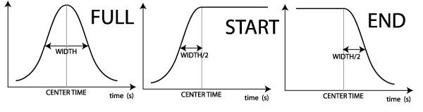
Advanced tab
| WARNING: This tab includes options that should only be changed if you are quite familiar with the meshing algorithm and techniques used. |
- SPATIAL INTERPOLATION: In FDTD generally, the electromagnetic field components are not recorded at the same point in space. Instead, each component of the vectorial electric and magnetic fields are recorded at different locations in the Yee cell. In order to properly calculate the Poynting vector and electromagnetic energy density, the fields are interpolated to the same location in the Yee cell. This setting controls how the fields are interpolated. With the NEAREST MESH CELL option (default for 'field and power' monitors), the fields are interpolated to the nearest FDTD mesh cell boundary. With the SPECIFIED POSITION option (default for 'profile' monitors), the fields are recorded exactly where the monitor is located. With NONE, no interpolation is performed and each electromagnetic field component is recorded at a different position within the Yee cell.
| Note: Spatial interpolation - NONE setting Disabling the spatial interpolation is a very advanced feature. Only expert users that are very familiar with the FDTD method should consider using this feature. Most standard analysis functions (such as the transmission script function, the data visualizer, etc) assume that the spatial interpolation is enabled. They may not give the most accurate result when used to analyze such monitor data. All analyses must be done manually. |
- RECORD DATA WITHIN PML: Collect monitor data within the PML boundary condition region. This is a very advanced option that should rarely be used. Contact Lumerical support before enabling this option. The simulation region - EXTEND STRUCTURE THROUGH PML option must be disabled when using this option.
Sampling frequency
OVERRIDE ADVANCED GLOBAL MONITOR SETTINGS: When this option is selected MIN SAMPLING PER CYCLE can be set. The other options cannot be altered, they are there to display settings.
- MIN SAMPLING PER CYCLE: This parameter determines the minimum amount of sampling per optical cycle that can be used. By default, it is set at 2 (the Nyquist limit) for optimum efficiency.
- DESIRED SAMPLING: This converts the minimum points per optical cycle into an actual sampling rate in Hz.
- NYQUIST LIMIT: The Nyquist sampling limit is calculated based on the maximum frequencies that may be present in the simulation volume.
- ACTUAL SAMPLING: The actual sampling rate is the rate that will actually be used for the discrete Fourier transforms (DFTs), taking into account the desired sampling rate, the Nyquist limit, and the time step, dt.
- DOWN SAMPLE TIME: This is the time step downsampling.
Results returned
Results
- E: Electric field data as a function of position and frequency/wavelength.
- H: Magnetic field data as a function of position and frequency/wavelength.
- P: Poynting vector as a function of position and frequency/wavelength.
- T: Transmission as a function of frequency/wavelength.
- FARFIELD: Farfield data can be obtained. For details about farfield settings, see the Simple far-field projection example.
Raw data
- POWER: Time-averaged power as a function of frequency. This data is only returned when a surface monitor (3D simulation) or line monitor (2D simulation) is used. For more information or an example using this data, see Parseval's theorem.
Mode expansion monitor - Simulation object
![]()
Mode Expansion Monitors use overlap analysis to calculate the forward/backward propagating components of any mode of a waveguide or fiber at an arbitrary location in the simulation region. The Mode Expansion monitor facilitates the interoperability between FDTD and INTERCONNECT as it returns the S parameters, which can be imported into INTERCONNECT directly. For more information and tips on best practices to get the most accurate results from this monitor, see using the mode expansion monitor.
Note that if performing parameter extraction using FDTD, using ports and the S-parameter sweep tool is preferable since the port objects can act as both sources and monitors and return S-parameters as a result.
Geometry tab
Monitor type: The monitor type and orientation, this option will control the available of spatial setting below
- X, Y, Z: The center position of the simulation region
- X MIN, X MAX: X min, X max position
- Y MIN, Y MAX: Y min, Y max position
- Z MIN, Z MAX: Z min, Z max position
- X SPAN, Y SPAN, Z SPAN: X, Y, Z span of the simulation region
The DOWN SAMPLE X, Y, Z option is used to set the spatial downsampling performed by the monitor. A down sample value of N corresponds to sampling (recording) the data every Nth grid points. Setting the down sample value to 1 gives the most detailed spatial information (i.e. information at each grid point).
Mode expansion tab
The Mode Expansion tab contains two main sections. The "Mode calculation" section allows users to select a mode (or a set of modes) to expand the input profile with. The "Monitors for expansion" section allows users to choose a field profile from an arbitrary monitor in the simulation to expand. For more information on this expansion calculation, and the results that are returned, see Using Mode Expansion Monitors.
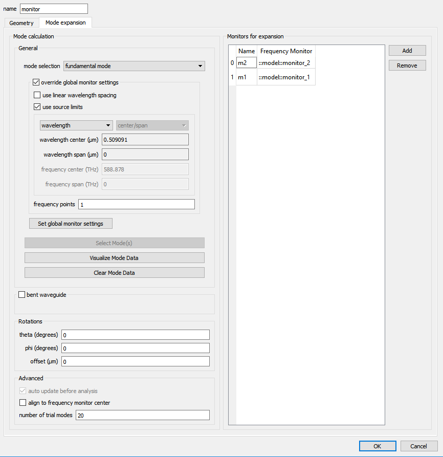
Mode Calculation
General
- MODE SELECTION: Allows users to select the modes to use for the mode expansion calculation. The "user select" option launches the eigenmode solver where the user can calculate and visualize the supported modes (see Mode analysis); use this option to select multiple modes. The eigenmode solver also provides a tool for frequency analysis (see Frequency Analysis - Modal Analysis Tab).
Following the "mode selection" combo box is a frame for choosing the frequencies to calculate the modes for. Note that this does not have to correspond to the frequency points for the monitors in the "Monitors for expansion" table. The mode expansion monitor will automatically perform the necessary interpolation between different frequency points.
- OVERRIDE GLOBAL MONITOR SETTINGS: A toggle to override the global monitor settings. If checked, the user can specify the frequency range and number of points at which the modes will be calculated at (using the options described below). If unchecked, the options below are set from the global monitor settings.
- SAMPLE SPACING: This combo-choice parameter determines how the sample frequency/wavelength will be selected. The three sample options are "uniform", "chebyshev" and "custom".
- USE WAVELENGTH SPACING: By default, data is recorded at certain spaced points with respect to frequency. Selecting this option spaces data at certain spaced points with respect to wavelength.
- USE SOURCE LIMITS: When checked these monitors use the source limits. When unchecked, the frequencies/wavelengths at which to record data can be set using the pull down menus and boxes below them.
- FREQUENCY POINTS: Set to choose the number of frequency points at which to record data.
When sample spacing is selected to be "custom", all the above settings will be disabled and a "custom frequency samples" table will be shown. Properties of the table are:
- ADD: Adds an entry above the selected entry to the "frequency (THz)" table
- REMOVE: Removes the selected entry from the "frequency (THz)" table
- SORT: Sorts the table with frequency from low to high
- SELECT MODE: If the "user selected" option has been chosen, this will bring up the Mode analysis tab for the user select from a calculated list of modes.
- VISUALIZE MODE DATA: This will bring up the Visualizer, showing all the profiles for the selected modes.
- CLEAR MODE DATA: Clears all the mode data.
Rotations
This frame allows user to apply an arbitrary rotation to the calculate modes.
- THETA: The angle of propagation, measured in degrees, with respect to the normal axis.
- PHI: The angle of propagation, in degrees, rotated about the normal axis in a right-hand context.
- OFFSET: Allows users to set an offset to the plane where the modes are calculated. This is useful for ensuring that monitors at an angle do not intersect with unwanted structures.
| Note: For best accuracy, we should place mode expansion monitors with rotations on a mesh cell. A useful approach is to add an override mesh region at the same position of the mode expansion monitor, and this override region can be infinitely thin (i.e., one of the spans can be '0'). |
Advanced
- AUTO UPDATE BEFORE ANALYSIS: If checked, the monitor will automatically update the chosen modes when "user select" in MODE SELECTION is selected. The monitor will find the best overlap between the chosen modes and the currently calculated modes, if there are a new set of modes. This allows users to keep track of the same chosen modes even the mode orders are switched, for example, when running a Parameter sweep over the waveguide width. This checkbox can be unselected but it has no effect if "fundamental mode", "fundamental TE mode" or "fundamental TM mode" is chosen in the MODE SELECTION dropdown list.
- ALIGN TO FREQUENCY MONITOR CENTER:
- By default, it is unchecked. In some cases, aligning to the center can lead to incorrect expansion when a monitor is offset. By unchecking this option, it performs the overlap calculation without aligning the center of the mode expansion monitor with the center of the frequency monitor. This feature is useful when a monitor, or both expansion and frequency monitor, is offset. For the best practice, when expanding the fields from a single frequency monitor, it is recommended to leave this unchecked and also to align the mode expansion monitor precisely with the frequency monitor that will be expanded, and with the center of the waveguide.
- If checked, the center of the mode expansion monitor will be laterally shifted to align with the center of the frequency monitor when the expansion is calculated. This makes it possible to use the same mode expansion monitor for the expansion of modes on different waveguides that are laterally offset. For example, using one mode expansion monitor to expand the modes in multiple channels that are laterally offset (e.g., drop and through) in a ring resonator simulation. It is recommended to place all monitors at the centers of the waveguides accordingly to avoid incorrect expansion. This shift does not add additional phase to the expansion.
- NUMBER OF TRIAL MODES: The number of modes specified to look for in order to find a fundamental mode. This will affect the modes that the solver finds. If this number is too small, the desired modes may not be found. Often, setting this number to 100 modes will ensure that no physical modes have been missed. If more than 100 modes exist, then a larger number should be used if one is interested in higher order modes.
Monitors for expansion
After the modes have been selected, the next step is to choose the monitor with the input field profile. The "Add" and "Remove" buttons on the side can be used to add/remove monitors, and users can choose the desired monitor from the monitor drop down list. See the getting Ring resonator getting started example for an example that uses mode expansion monitor.
| Notes: Advanced setup tips for best results
|
Results returned
Modes
- NEFF: Effective index as a function of selected mode and frequency/wavelength is returned.
- MODE PROFILES: Mode profiles (E, H, and index) as a function of position and frequency/wavelength.
Modal expansions
- EXPANSION FOR: A set of expansion results are returned for each input monitor specified under "Monitors for expansion". Each set of result contains Ttotal, Tforward,Tbackward, Tnet, a,b, N, and P. Please see the Using Mode Expansion Monitors page for more information.
Using and understanding Mode Expansion Monitors
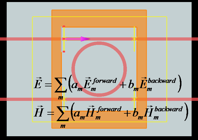
Mode expansion monitor simulation objects allow you to analyze the fraction of power transmitted into any mode(s) of a non-absorbing waveguide or fiber. This page provides additional information to allow users to get the most accurate results from their simulations. See the Mode expansion monitor page for an overview of these objects and lists all input and output properties.
Note that if performing parameter extraction using FDTD, using ports and the S-parameter sweep tool is preferable since the port objects can act as both sources and monitors and return S-parameters as a result.
What is mode expansion?
Consider a waveguide/fiber that supports a set of forward-propagating modes, φforward m
(with Eforwardm and Hforwardm ), and backward-propagating modes, φbackward m (with Ebackwardm and Hbackwardm
). If a complete basis state of modes is known, any input field can be expanded using these modes:
Ein=∑m(amEforwardm+bmEbackwardm)
Hin=∑m(amHforwardm+bmHbackwardm)
am
and bm
represent the complex transmission coefficient of the forward and backward propagating waves respectively. The forward and backward propagating modes are related by symmetry:
E backward m=Eforwardt,m−Eforwardz,m^z
H backward m=−Hforward t,m+Hforwardz,m^z
where we decomposed Eforwardm
in a transverse component Eforwardt,m and longitudinal component Ebackwardz,m (assuming the modes propagate in the z direction), and similarly for Hforwardm. Thus, we can rewrite the expressions above for the input fields completely in terms of forward-propagating modes and simplify the notation by dropping the forward/backward notation and using φm (with Em and Hm
) for the forward-propagating modes. If we assume power orthogonality of these modes according to
〈φm|φn〉≡0.5∗∫dS⋅Em×H∗n=Nmδmn
then the coefficients for any mode m
can be determined from the overlap integrals:
0.5∗∫dS⋅Ein×H∗m=(am+bm)Nm
0.5∗∫dS⋅E∗m×Hin=(am−bm)N∗m
This is the basic concept behind mode expansion monitors. The user can specify an arbitrary input field Ein
and Hin (recorded by a frequency monitor), and modal fields Em and Hm
(by a mode expansion monitor). The mode expansion monitor will return the following results:
am=0.25∗(∫dS⋅Ein×H∗mNm+∫dS⋅E∗m×HinN∗m)
bm=0.25∗(∫dS⋅Ein×H∗mNm−∫dS⋅E∗m×HinN∗m)
Nm=0.5∗∫dS⋅Em×H∗m
Pin=0.5∗∫dS⋅Ein×H∗in
where Re(Nm)
is the power of the mode m in the waveguide, and Re(Pin)
is the total input power (in Watt) recorded by the frequency monitor. The script function expand can also be used to perform this type of mode expansion.
| Note: Grid dispersion These equations only apply to the ideal case. In practice, since an FDTD simulation uses a mesh, a correction step is necessary to account for the grid dispersion from this discrete mesh. This correction factor is taken into account in the mode expansion monitor built-in analysis. In the limit where the mesh size gets very very small, these equations will give the same results as the mode expansion monitor with the built-in correction. |
| Note: Power orthogonality Strictly speaking, the power orthogonality condition using the conjugated cross product above is true for the bound modes of non-absorbing waveguides. A more general orthogonality relation, valid for both absorbing and non-absorbing waveguides, is based on the unconjugated cross product: 0.5∗∫dS⋅Em×Hn=N∗mδmn |
| This approach is implemented in the script function expand2. It happens that for bound modes of non-absorbing waveguides, E and H (transverse to the direction of propagation) are real valued. Therefore the unconjugated and conjugated expressions for non-absorbing waveguides are the same, and the modes are power orthogonal. However, the disadvantage of this approach is that without the complex conjugate of the H-field, the normalization constant cannot be associated with the power carried by the waveguide modes, eg, of absorbing waveguides. |
How to set up mode expansion monitors
The mode expansion monitor must be placed over the cross section of the waveguide/fiber that supports the modal fields. The monitors that are being expanded by the mode expansion monitor must also be placed over the same cross section. Once this is done, the Mode Expansion tab can be used to select the input profiles ( Ein
,Hin ), and the modal fields ( Em, Hm
). For a description on the individual settings in this tab, see Mode Expansion.
Modal Fields
When you edit mode expansion monitor, the “Mode calculation” section is for selecting the modal fields for this expansion. The fundamental mode is sufficient for most cases, but if you would like to calculate the expansion coefficient for multiple modes, select “user select” from the drop down menu, and then click on “Select Mode”. This will bring up the mode solver and you can choose any mode(s) for this calculation from the mode list. You may also want to use more than 1 frequency points if the component has a wide operation bandwidth.
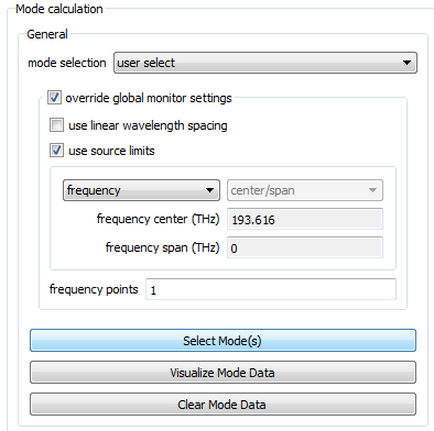
Input profiles
We use a frequency monitor as the input profile (the profile to be expanded). The “Monitors for expansion” section allows users to choose the monitors that contain the input profiles. In the example below, four input profiles have been selected (corresponding to each port of the ring resonator). This means that 4 sets of expansion coefficients will be available in the Mode Expansion's results section.
What do the results mean?
The results that can be obtained from a mode expansion monitor is shown in the screen shot below:
A set of expansion results will be available for each input monitor specified under "Monitors for expansion". Each set of result contains:
| Ttotal | the total transmission of the input profile. This will be the same as the result obtained with the transmission script command. It's important to notice that the Transmission values are normalized to the power injected by the source. |
| Tforward | the forward (the direction of the positive coordinate axis) transmission into the selected modal field(s). If more than 1 mode had been selected under "Mode calculation", the result will be an array containing the forward transmission into each mode. |
| Tbackward | the backward (the direction of the negative coordinate axis) transmission into the selected modal field(s) |
| Tnet | the net transmission into the selected modal field(s) |
| a | complex transmission coefficient of the forward propagating waves, of the selected model field(s) |
| b | complex transmission coefficient of the backward propagating waves, of the selected model field(s) |
| N | the power of the mode in the waveguide, based on the peak modal |E|^2 =1 in w2, this power changes with the area of the modal field. |
| P | the total input power recorded by the frequency monitor, in Watt. |
| Note: No results returned If no results are returned in the mode expansion monitor, the most likely cause is that no "Monitors for expansion" have been selected, or that they are of the wrong type (ex. if they do not have the right dimensions or surface normal). |
Interpreting the results
Often, we are only interested in a single waveguide cross section and a single mode. In this case, it is very straight forward to interpret the expansion results. For example, in expansion1.fsp, we have a very simple set up with a mode source injected into a dielectric waveguide.
In this case, we have Tforward=|a|2Nsourcepower∼1
(ie. the forward transmission into the fundamental mode of the waveguide) and Tbackward=|b|2Nsourcepower∼0 for the "T" monitor in front of the source. For the "R" monitor behind the source, we have Tforward=Tbackward=0
, since there are no reflections in this setup.
However, if you have multiple waveguide cross section geometries in the simulation (ex. Grating Coupler), or if you are expanding the fields using a different mode than what was injected by the source, the interpretation is less obvious. The reason is because when the mode expansion monitor is calculating the modal fields of the structure, the mode amplitude is arbitrary and the fields are simply scaled such that the peak |E|^2 value is 1 with a phase of 0. One consequence of this scaling is that the amount of power in each mode can be different. For example, a mode with a larger spatial size will tend to carry more power than a smaller mode, simply because they have the same peak intensity but are different in size. This power, N, can be calculated by integrating the Poynting vector of the modal fields. In some situation, N can be larger than the input power P. The reason is that N is calculated based on the peak modal |E|^2 =1 in w2, so N increases with the cross-sectional area of w2.
For example, in expansion2.fsp, the fundamental mode at the narrow waveguide (w1) is used as the source, and we want to study the transmission into the wide waveguide (w2).
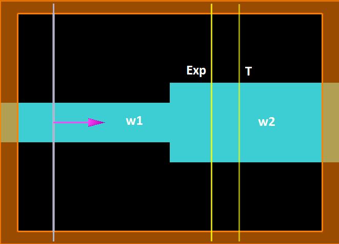
When the mode source injects the fundamental mode into w1 at the injection plane (with a peak amplitude of 1 V/m and a phase of 0), it will inject a fixed amount of power in Watts, which we can calculate from the sourcepower function. An expansion monitor "Exp" and a field monitor "T" has been set up in w2 that will be used to study the transmission into the wide waveguide. Since the expansion monitor is positioned in w2, it will expand the fields based on the fundamental mode of w2, which is different than the mode injected by the source. Again, the peak amplitude of the mode from the expansion monitor will be normalized to 1 V/m. The expansion monitor then calculates , which is the overlap integral between the fields recorded by "T" and the mode profile from "Exp". However, the raw value is not meaningful because the normalization applied to the mode from the expansion monitor is completely arbitrary. What we need to do is to normalize away the fact that the different modes contain different amounts of power.
The fraction of power transmitted into the fundamental mode of w2 is actually:
Tforward=|aout|2Nout|ain|2Nin
where
- aout
- : the arbitrary complex transmission coefficient of the selected mode in w2
- ain
- : the complex transmission coefficient of the selected mode in w1
- Nout
- : the power contained in the selected mode in w2
- Nin
- : the power contained in the selected mode in w1
- |aout|2Nout
- : the actual forward transmitted power that the selected mode carries in w2.
Ie. the coupling coefficients must be scaled by the power for each mode. Nout
is returned as a result for "Exp", and Nin can be obtained from the sourcepower command (and ain
equals 1). The equation above becomes:
|aout|2Noutsourcepower
The script expansion2.lsf calculates this value, and as expected, this is exactly what the result "T forward" from the expansion monitor returns.
Parameter extraction
The mode expansion monitors allows users to extract the complex transfer function of an element since their results contain the necessary amplitude and phase information. However, if using FDTD, using the port objects in conjunction with the S-parameter sweep tool is recommended since they make it easy to set up and automate the S-parameter extraction without needing to set up separate sources and monitors at each port of the device. For a step-by-step tutorial on how to carry out this process, see the Ring Resonator Tutorial in FDTD Solutions and MODE Solutions.
When using the varFDTD solver in MODE, a combination of sources, field monitors and mode expansion monitors can be used to extract the S-parameters which serve as the interface between the physics-based, component level simulations and the system/circuit level simulations that involve multiple components in arbitrarily complex configurations.
Related publications
- A. W. Snyder and J. D. Love, "Optical Waveguide Theory". London: Kluwer Academic Publishers (1983).
Understanding time apodization in frequency domain monitors
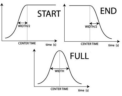
This page describes the apodization option of Frequency monitors. Apodization makes it possible to exclude effects that occur near the start and/or end of the simulation from the monitors fourier transform.
This feature can be useful for filtering away short lived transients that occur when a system is excited with a dipole source, and when studying high Q systems that decay very slowly. Apodization is considered to be an advanced feature and care must be taken when using it. Do some testing with a simple test simulation first, to make sure you understand how the monitor apodization affects your simulation results.
Monitor apodization applies a window function to the simulation fields E(t) before the monitor performs its Fourier transform of E(t) to obtain E(w). This makes it possible to calculate E(w) from a portion of the time signal. For example, start apodization can be used to ignore all transients which occur near the start of the simulation.
| Note: Apodization will, in general, invalidate any source normalization performed and is therefore not suitable for accurate power or absolute field intensity measurement. For some resonant cavities, the absolute field intensities can be obtained with a bit of extra work. Details can be found in Correcting field amplitudes |
Full Apodization
This example shows how to use start apodization to get the correct mode profile for a photonic crystal cavity contained in usr_Tang_cavity.fsp. The simulation contains dipoles which are used to excite the modes of the cavity and a frequency monitor is set up to get the mode profile of the A11 mode.
Let's begin by looking at the electric field as a function of time. In particular, the blue line in the figure below shows |E|2 from the m2 time monitor. The transients at the beginning are due to all the energy injected by the dipoles which is not coupled into the A11 mode. For times greater than 600fs the time signal decays exponentially due to the fact that the majority of the energy left in the simulation is left in the cavity modes. The beating in the time signal is due to the fact that there are two cavity modes which are excited whose resonance frequencies do not lie far apart.
In order to plot mode profile for the A11 from a frequency monitor we need to use start apodization to get rid of the transients. The green line in the plots above shows the apodization window function used in the A11 monitor in the simulation. Note that the center time of the window function is set to 1000fs in order to ensure that most of the energy in the cavity is contained in the mode. The resulting mode profile is shown to the left below.
What happens if you do not use start apodization? The simulation contains a copy of the A11 monitor in which there is no apodization. This monitor is called A11_no_apodization. The magnitude of the electric fields are plotted in the image below to the right. In this image, you can see a superposition of the mode profile and the fields from the transients. The effect of the transients is most apparent at location of the sources.
Note that there are two sources in the simulation. They are placed at the origin of simulation and at x = 500nm, y = 400nm. However, since symmetry was used in the simulation the source at x = 500nm, y = 400nm is mirrored across the x and y axes. In the image below only three of the sources are pointed out (so that it is easier to see the mode profile).
| Start Apodization  | No Apodization 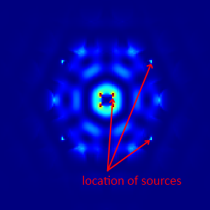 |
The end apodization does not have a visible affect in this simulation. To see that this claim is true, plot the electric field intensity from the A11_end_apodization monitor in the simulation. This monitor is the same as the A11 monitor except that it only uses end apodization, and the resultant |E|2 plot looks like the plot from the monitor without any apodization.
Spectral averaging simple example
 This page provides a simple example of the spectral averaging feature of frequency domain field monitors. This feature provides the most efficient method for calculating the average response over a range of frequencies.
Power monitors have three spectral averaging modes.
- Standard Fourier Transform (SFT), or no averaging. This is the default option, which calculates the response of the system at a particular set of frequencies.
- Partial Spectral Average (PSA). This option calculates the average response over a range of frequencies using a Lorentzian weighting function.
- Total Spectral Average (TSA). This option calculates the average response over the entire source spectrum.
The options can be selected in the Data to record tab of the monitor properties, as shown below.
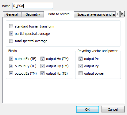
In this example, we will calculate the reflection of an Air-Si-Ag-Air multi-layer stack in FDTD (a similar set up can be created in MODE' propagator). This is a useful test case because it has a complicated reflection spectrum. A screenshot of the structure is shown below. Please note that for this multilayer problem we have set the mesh refinement to "conformal variant 1" to take full advantage of the conformal meshing for both the Si and the Ag layer.
Without the spectral averaging functions (PSA and TSA), the only way to calculate an average spectral response is to measure the response at a large number of frequencies with the Standard Fourier Transform (SFT) option, then manually calculate the averages by post processing. The problem with this technique is that the simulation memory requirements can become impractically large when attempting to save a large number of frequencies.
In this example, we will calculate two values.
- Average reflection at 50 frequency points between 350-750HTz using a 10THz FWHM Lorentzian weighting function.
- Total average reflection between 350-750THz.
Both calculations will be done by two techniques.
- The built in PSA and TSA monitor options.
- The brute force technique of using a SFT monitor to measure the response at many frequencies (500). The average can then be manually calculated.
The following figure shows the memory requirements estimate of this simulation. Notice that the SFT monitor measuring 500 frequency points requires 66% of the memory, while the PSA monitor requires only 7% and the TSA requires 0.1%. In large 3D FDTD simulations, the memory savings from the PSA and TSA options can be very important.
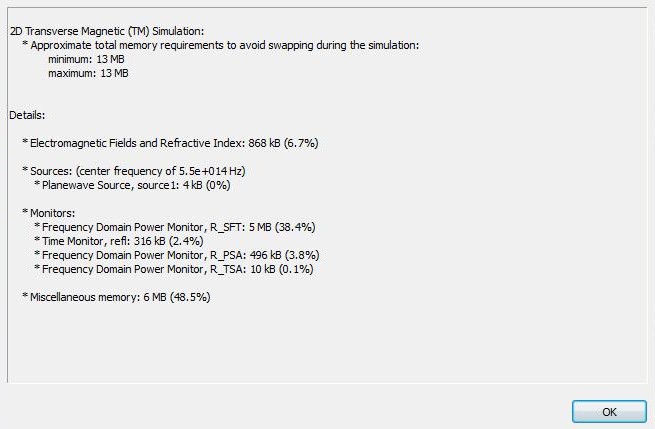
Standard fourier transform (SFT)
The Standard fourier transform (SFT) calculates the response of the system at a set of specific frequencies. The vast majority of simulation analysis uses the SFT mode of operation.
The following figure shows the reflectance as a function of frequency at 500 points between 350-750 THz.
For more details about how the SFT is calculated, see the Frequency domain normalization section of the Reference Guide.
Partial spectral average (PSA)
The Partial spectral average (PSA) mode of operation allows the monitor to calculate the average response of the system over a range of frequencies. The weighting function is the product of the source spectrum and a lorentzian. The FWHM of the lorentzian can be specified in the monitor properties. In this example, it is 10THz.
The following figure shows the average reflectance as calculated by the PSA monitor (red) and the brute force technique (green). The two techniques give very similar results, although there are some differences at the minimum and maximum frequencies. The differences at these frequencies occur because the SFT data does not contain any data beyond the minimum or maximum frequencies. One other very important difference is that the brute force technique required 10 times more simulation memory.
The reflectance vs frequency as calculated by the SFT (blue) is shown for reference. The lorentzian weighting function (10 THz wide, centered at 530 THz) is also shown for reference.
NOTE: Discrepancies between PSA and brute force technique at the min and max frequencies
The brute force calculation does not include reflected power beyond the source limits (<350THz and >750THz), while the TSA monitor includes all frequencies in the integrals. If the frequency range of the standard fourier transform (SFT) monitor was increased, the agreement would improve.
Total spectral average (TSA)
The Total spectral average (TSA) mode of operation allows the monitor to calculate the average response of the system using the source spectrum as a weighting function.
The following figure shows the average reflectance as calculated by the TSA monitor (red) and the brute force technique (green). The two techniques give very similar results. One very important difference is that the brute force technique required 500 times more simulation memory.
NOTE: Discrepancy between TSA and brute force technique
The brute force calculation does not include reflected power beyond the source limits (<350THz and >750THz), while the TSA monitor includes all frequencies in the integrals. If the frequency range of the standard fourier transform (SFT) monitor was increased, the agreement would improve.


 3433
3433


 被折叠的 条评论
为什么被折叠?
被折叠的 条评论
为什么被折叠?
 到【灌水乐园】发言


