


ADUCM331开发笔记(四)ADC使用说明
- 6 ADC使用说明
- 6.1 ADC OVERVIEW模数转换器概览
- 6.2 ADC OPERATION模数转换器操作
- 6.2.1 Power Modes模数转换器电源模式
- 6.2.2 ADC Normal Power Mode模数转换器正常电源模式
- 6.2.3 ADC Low Power Mode模数转换器低功耗模式
- 6.2.4 Bipolar/Unipolar Configuration模数转换器双极/单极配置
- 6.2.5 Typical ADC Modes of Operation典型模数转换器工作模式
- 6.2.6 Conversion Modes转换模式
- 6.2.7 ADC Idle Mode空闲模式
- 6.2.8 Power-Down Mode关断模式
- 6.2.9 Modifying ADC Settings更改模数转换器设置
- 6.2.10 ADC Power-Up Sequence模数转换器上电时序
- 6.3 ADC CALIBRATION模数转换器标定
- 6.4 ADC SINC3 DIGITAL FILTER RESPONSE模数转换器sinc3数字滤波器响应
- 6.5 DIGITAL FILTER OPTIONS模数转换器数字滤波器选项
- 6.6 ADC CONFIGURATION模数转换器配置
- 6.7 IADC DIAGNOSTICS电流模数转换器诊断
- 6.8 OTHER ADC SUPPORT CIRCUITS其他模数转换器支持电路
- 6.9 ADC CHOPPING模数转换器斩波
- 6.10ADC REGISTERS模数转换器寄存器
- 6.10.1 ADC Status Register (Table 83)模数转换器状态寄存器
- 6.10.2 ADC Mask Register (Table 84)模数转换器屏蔽寄存器
- 6.10.3 ADC Mode Register (Table 85)模数转换器模式寄存器
- 6.10.4 ADC Control Register: ADC0CON (Table 86)模数转换器控制寄存器ADC0CON
- 6.10.5 ADC Control Register: ADC1CON (Table 87)模数转换器控制寄存器ADC1CON
- 6.10.6 ADC Filter Register (Table 88)模数转换器滤波器寄存器
- 6.10.7 ADC Configuration Registers (Table 89)模数转换器配置寄存器
- 6.10.8 ADC Data Register (Table 90 and Table 91)模数转换器数据寄存器
- 6.10.9 ADC Calibration Registers模数转换器校准寄存器
- 6.10.10 ADC Offset Registers (Table 92, Table 93, and Table 94)模数转换器偏移寄存器
- 6.10.11 ADC Gain Registers (Table 95, Table 96, and Table 97)模数转换器增益寄存器
- 6.10.12 ADC Current Channel Accumulator: ADC0ACC (Table 103)模数转换器电流通道累加器
- 6.11 ADC MEMORY MAPPED REGISTERS模数转换器内存映射寄存器列表
6 ADC使用说明
ADuCM330/ADuCM331 Hardware Reference Manual UG-716
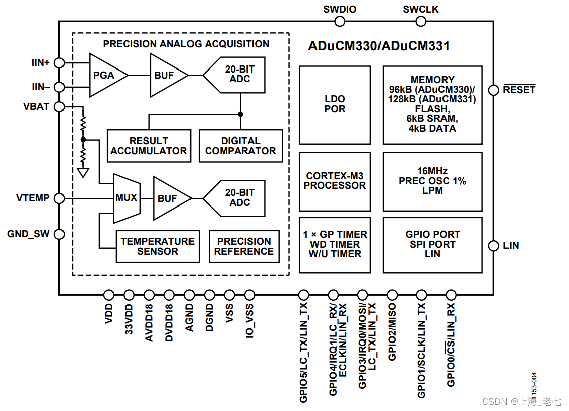
FEATURES
- High precision analog-to-digital converters (ADCs)
- Dual channel, simultaneous sampling
- I-ADC 20-bit Σ-Δ (minimizes range switching)
- VADC/TADC 20-bit Σ-Δ
- Programmable ADC conversion rate from 1 Hz to 8 kHz
- On-chip ±5 ppm/°C voltage reference
- Current channel
- Fully differential, buffered input
- Programmable gain (from 4 to 512)
- ADC absolute input range: −200 mV to +300 mV
- Digital comparator with current accumulator feature
- Voltage channel
- Buffered, on-chip attenuator for 12 V battery input
- Temperature channel
- External and on-chip temperature sensor options
6.1 ADC OVERVIEW模数转换器概览
The ADuCM330/ADuCM331 incorporate two Σ-Δ, analog-to-digital converters (ADCs). ADC0 is a 20-bit (19 data bits, 1 sign bit) current ADC (IADC). ADC1 is a 20-bit voltage/temperature ADC (VADC/TADC).
These precision measurement channels integrate attenuator, on-chip buffering; a programmable gain amplifier; Σ-Δ modulators; and digital filtering for precise measurement of current, voltage, and temperature variables in 12 V automotive battery systems.
ADuCM330/ADuCM331集成了两个Σ-Δ型模数转换器(ADC0和ADC1)。ADC0 为 20 位(19 个数据位,1 个符号位)的电流ADC(IADC)。ADC1是一款20位电压/温度ADC (VADC/TADC)。
这些精密测量通道集成了衰减器、片上缓冲;可编程增益放大器;Σ-Δ调制器;和数字滤波,用于精确测量 12 V 汽车电池系统中的电流、电压和温度变量。
The simplified ADC transfer function can be described as follows.
简化的ADC传递函数可以描述如下。
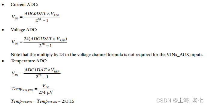
To use the factory calibrated gain coefficient for the internal temperature sensor, copy the value from memory location 0x000207EA into the ADC2GN register. The factory default offset coefficient is held at location 0x000207E8.
Four options are available for the ADC reference voltage:
• External reference to the VREF pin (default configuration)
• Internal reference (1.2 V) to AGND
• AVDD18 to AGND
• AVDD18 to GND_SW for temperature channel
The supply voltage is 1.8 V from the LDO. The two ADCs can independently select a different reference or the same reference.
Note that if using the internal 1.2 V reference, ensure that the ADC reference and reference buffer are enabled via the HRFCTRL and IRFPD registers.
要对内部温度传感器使用工厂校准的增益系数,请将该值从存储器位置0x000207EA复制到ADC2GN寄存器中。出厂默认偏移系数保留在位置 0x000207E8。
ADC基准电压有四种选择:
• VREF引脚的外部基准(默认配置)
• 内部基准电压源 (1.2 V) 至 AGND
• AVDD18 至 AGND
• AVDD18 至 GND_SW 用于温度通道
电源电压为LDO的1.8 V。两个ADC可以独立选择不同的基准电压源或相同的基准电压源。
请注意,如果使用内部1.2 V基准电压源,请确保通过HRFCTRL和IRFPD寄存器使能ADC基准电压源和基准电压缓冲器。
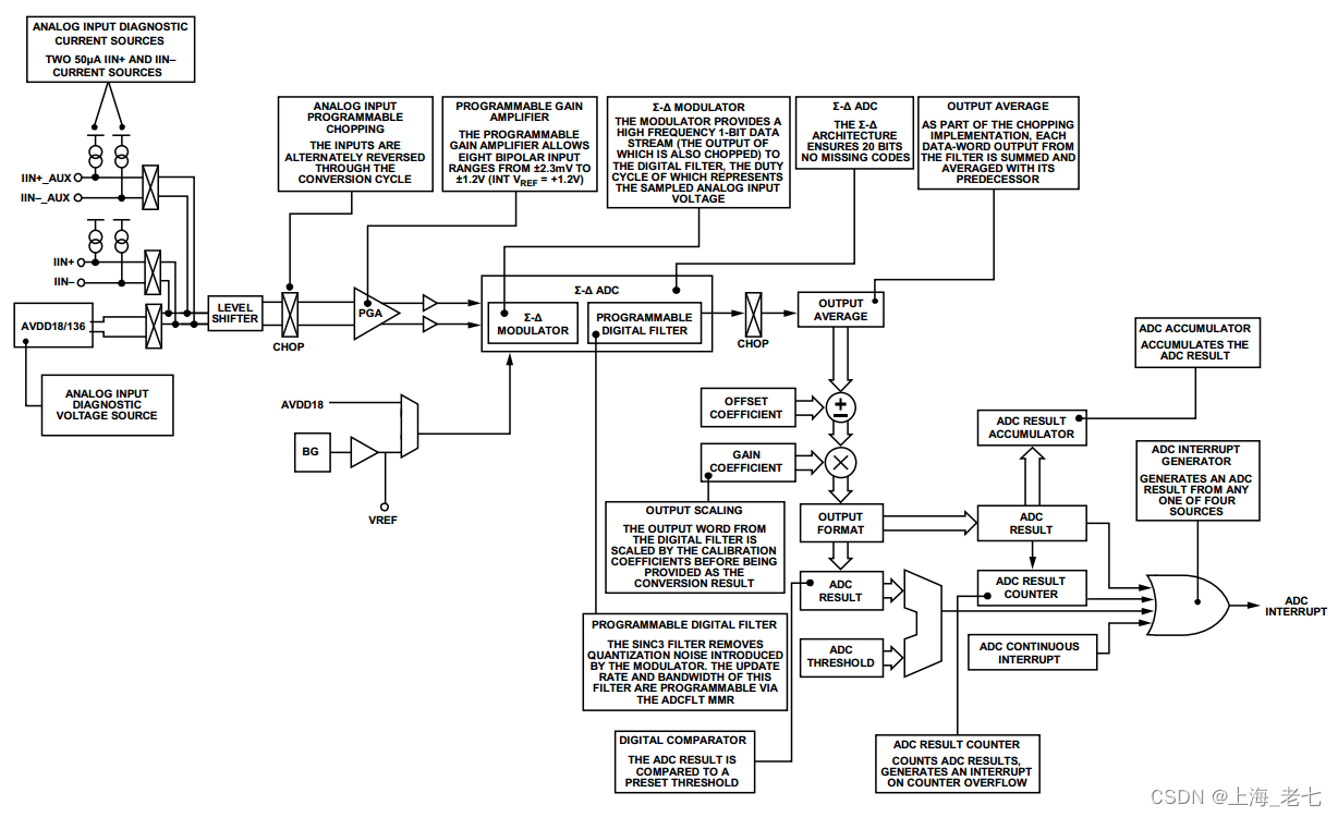
6.1.1 Current ADC (IADC)电流模数转换器
The IADC converts battery current sensed through, for example, an external 100 μΩ shunt resistor. On-chip programmable gain means that the IADC can be configured to accommodate battery current levels of up to ±1500 A.
As shown in Figure 10, the IADC employs a Σ-Δ conversion technique to realize 19 bits plus a sign bit of no missing codes performance.
There are four pairs of input differential signals, which are selected inside the input mux:
• IIN+/IIN−
• IIN+/IIN− (internal short configuration)
• (AVDD18/136)/GND (voltage input to diagnostic)
• IIN+_AUX/IIN−_AUX (auxiliary channel)
The Σ-Δ modulator converts the sampled input signal into a digital pulse train, whose duty cycle contains the digital information. A modified sinc3 or sinc4, programmable, low-pass filter is employed to decimate the modulator output data stream to give a valid 20-bit data conversion result at programmable conversion rates from 10 Hz to 8 kHz in normal mode and 1 Hz to 656 Hz in low power mode.
The IADC also incorporates a counter, comparator, and accumulator logic. This allows the IADC result to generate an interrupt after a predefined number of conversions have elapsed, or if the IADC result exceeds a programmable threshold value. When enabled, a 32-bit accumulator automatically sums the 20-bit IADC results.
The time to a first valid (fully settled) result on the current channel is three ADC conversion cycles, with chop mode turned off, and two ADC conversion cycles, with chop mode turned on. An interrupt can be generated even on unsettled ADC samples by enabling the ADC continuous interrupt option.
电流ADC用于转换通过外部100 μΩ分流电阻等方式检测到的电池电流。片上可编程增益意味着 IADC 可以配置为适应高达 ±1500 A 的电池电流水平。
如图10所示,IADC采用Σ-Δ转换技术,实现19位加1位标志位的无丢失编码性能。
电流ADC可以有四对输入差分信号,这些信号在输入多路复用器内进行选择:
• IIN+/IIN−
• IIN+/IIN− (内部短路配置)
• (AVDD18/136)/GND(用于诊断的电压输入)
• IIN+_AUX/IIN−_AUX (辅助通道)
Σ-Δ调制器将采样的输入信号转换为数字脉冲序列,其占空比包含数字信息。采用改进的sinc3或sinc4可编程低通滤波器对调制器输出数据流进行抽取,以正常模式下10 Hz至8 kHz和低功耗模式下1 Hz至656 Hz的可编程转换速率提供有效的20位数据转换结果。
电流ADC还集成了计数器、比较器和累加器逻辑。这允许电流ADC的结果在经过预定的转换次数后产生中断,或在电流ADC采样结果超过可编程阈值时产生中断。使能此功能后,32 位累加器会自动对 20 位 IADC 结果求和。
电流通道产生第一个有效(完全建立)结果的时间为三个ADC转换周期(斩波模式关闭)和两个ADC转换周期(斩波模式开启)。通过启用ADC连续中断选项,即使在未建立的ADC采样上也可以产生中断。
6.1.2 Voltage/Temperature ADC (VADC/TADC) 电压温度模数转换器
The VADC/TADC converts additional battery parameters, such as voltage and temperature. The input to this channel can be multiplexed from an external voltage and an on-chip temperature sensor.
There are five different input signal pairs, which are selected inside the input mux:
• VBAT/AGND (VBAT attenuator selected)
• VTEMP/GND_SW (external temperature sensor)
• Vbe1/Vbe2 (internal temperature sensor)
• VINP_AUX/VINM_AUX (auxiliary voltage input)
• Vbe/GND (VIN for ADC diagnostic)
VADC/TADC 转换外部的电池参数,例如电压和温度。该通道的输入可以多路复用来自于外部的电压和片上温度传感器。
VADC/TADC采样有五对不同的输入信号,这些输入信号在输入多路复用器中选择:
• VBAT/AGND(已选择VBAT衰减器)
• VTEMP/GND_SW(外部温度传感器)
• Vbe1/Vbe2 (内部温度传感器)
• VINP_AUX/VINM_AUX (辅助电压输入)
• 电压/接地(用于 ADC 诊断的 VIN)
As with the current ADC, the VADC/TADC employs an identical Σ-Δ conversion technique, including a modified sinc3 or sinc4 low-pass filter to give a valid 20-bit data conversion result at programmable output rates from 4 Hz to 8 kHz in normal mode and 1 Hz to 656 Hz in low power mode. An external RC filter network is not required, because this is internally implemented in the voltage channel.
The external battery voltage (VBAT) is routed to the ADC input via an on-chip, high voltage (divide by 24), resistive attenuator. This ADC channel, unlike the current channel, has a fixed input range of 0 V to 28.8 V on VBAT.
The battery temperature can be derived through the on-chip temperature sensor.
By default, the time to a first valid (fully settled) result after an input channel switch on the voltage/temperature channel is three ADC conversion cycles, with chop mode turned off. A top level overview of the ADC signal chain is shown in Figure 11.
与电流ADC一样,VADC/TADC采用相同的Σ-Δ转换技术,包括改进的sinc3或sinc4低通滤波器,以正常模式下4 Hz至8 kHz的可编程输出速率和低功耗模式下1 Hz至656 Hz的可编程输出速率提供有效的20位数据转换结果。不需要外部RC滤波器网络,因为这是在电压通道内部实现的。
外部电池电压 (VBAT) 通过片内高压(除以 24)阻性衰减器路由到 ADC 输入。与电流通道不同,该ADC通道在VBAT上具有0 V至28.8 V的固定输入范围。
电池温度可以通过片上温度传感器采样得出。
默认情况下,输入通道在电压/温度通道上切换后,获得第一个有效(完全建立)结果的时间是斩波模式关闭下的三个ADC转换周期。ADC信号链的顶层概述如图11所示。
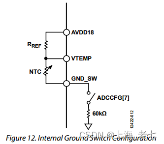
6.1.3 ADC Ground Switch模数转换器的接地开关
The ADuCM330/ADuCM331 feature an integrated ground switch pin, GND_SW. This switch allows the user to dynamically disconnect ground from external devices and allows a connection to ground using a 60 kΩ resistor, reducing the number of external components required for an NTC circuit, as shown in Figure 12. The control bit for this switch is ADCCFG[7]. The ground switch feature can be used for reducing power consumption on application specific boards.
ADuCM330/ADuCM331具有一个集成的接地点选择引脚GND_SW。该开关允许用户动态断开与外部设备的接地,并允许使用60 kΩ电阻连接到地,从而减少NTC电路所需的外部元件数量,如图12所示。该开关的控制位为 ADCCFG[7]。接地开关功能可用于降低特定应用电路板的功耗。
6.1.4 ADC Noise模数转换器采样噪声
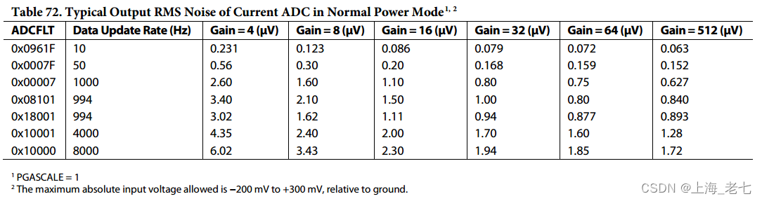
Table 72 lists the output rms noise in microvolts for some typical output update rates on the IADC. The numbers are typical and are generated at a differential input voltage of 0 V. The output rms noise is specified as the standard deviation (or 1 ∑) of the distribution of ADC output codes collected when the ADC input voltage is at a dc voltage. It is expressed in microvolts rms (µV rms).
表72列出了IADC上一些典型输出更新速率的输出均方根噪声(以微伏为单位)。这些数字是典型的,是在0 V差分输入电压下产生的。输出均方根噪声指定为ADC输入电压处于直流电压时收集的ADC输出代码分布的标准偏差(或1 ∑)。它以微伏均方根(μV rms)表示。
6.2 ADC OPERATION模数转换器操作
6.2.1 Power Modes模数转换器电源模式
Two power modes are available on the ADuCM330/ADuCM331:
• Normal mode
• Low power mode
The ADCs can be configured into reduced (low power) or full power (normal) mode of operation by configuring ADCMDE[3] as appropriate. The Cortex-M3 processor can also be configured in low power modes of operation (PWRMOD[2:0]). The processor power modes are independently controlled and are not related to the ADC power modes described in the following sections.
ADuCM330/ADuCM331提供两种功耗模式:
• 正常模式
• 低功耗模式
通过根据需要配置 ADCMDE[3],可将 ADC 配置为降低(低功耗)或全功率(正常)工作模式。
请注意,Cortex-M3 处理器也可以配置为低功耗工作模式 (PWRMOD[2:0])。处理器电源模式是独立控制的,与以下各节中描述的 ADC 电源模式无关。
6.2.2 ADC Normal Power Mode模数转换器正常电源模式
In normal mode, the current and voltage/temperature channels are fully enabled. The ADC modulator clock is 512 kHz and enables the ADCs to provide regular conversion results at a rate of between 10 Hz and 8 kHz. Both channels are under full control of the core and can be reconfigured at any time. The default ADC update rate for all channels in this mode is 1 kHz.
The IADC and VADC/TADC channels can be configured to initiate periodic, normal power mode, high accuracy, and single conversion cycles before returning to ADC full power-down mode. This flexibility is facilitated under full core control via the ADCMDE MMR, and ensures that continuous periodic monitoring of battery current, voltage, and temperature settings is feasible while ensuring that the average dc current consumption is minimized.
在正常模式下,电流和电压/温度通道完全启用。ADC调制器时钟为512 kHz,使ADC能够以10 Hz至8 kHz的速率提供常规转换结果。两个通道都完全由内核控制,可以随时重新配置。此模式下所有通道的默认ADC更新速率为1 kHz。
IADC和VADC/TAPC通道可配置为在返回ADC完全关断模式之前启动周期性正常功率模式、高精度和单次转换周期。在通过ADCMDE MMR进行全内核控制的情况下,这种灵活性得到了促进,并确保对电池电流、电压和温度设置进行连续的定期监控是可行的,同时确保将平均直流电流消耗降至最低。
6.2.3 ADC Low Power Mode模数转换器低功耗模式
In ADC low power mode, the IADC is enabled in a reduced power and reduced accuracy configuration. The ADC modulator clock is 128 kHz and enables the ADCs to provide regular conversion results at a rate of between 1 Hz to 656 Hz. All of the ADC peripheral functions (result counter, digital comparator, and accumulator) can be enabled in low power mode, requiring no extra power. Low power mode is designed for gains of 64 to 512 specifically.
Typically, in low power mode, the IADC only is configured to run at a low update rate and to continuously monitor battery current. The processor is in power-down mode and wakes up when the IADC interrupts the core. This interrupt occurs when the IADC detects a current conversion beyond a preprogrammed threshold, a set point, or a set number of conversions.
在ADC低功耗模式下,IADC以低功耗和降低精度配置使能。ADC调制器时钟为128 kHz,使ADC能够以1 Hz至656 Hz的速率提供常规转换结果。所有ADC外设功能(结果计数器、数字比较器和累加器)均可在低功耗模式下使能,无需额外功耗。低功耗模式专为 64 至 512 的增益而设计。
通常,在低功耗模式下,IADC仅配置为以低更新速率运行并持续监测电池电流。处理器处于掉电模式,并在 IADC 中断内核时唤醒。当空间碎片协委会检测到电流转换超过预编程阈值、设定点或设定转换次数时,就会发生此中断。
6.2.4 Bipolar/Unipolar Configuration模数转换器双极/单极配置
The analog inputs to the ADuCM330/ADuCM331 can accept either unipolar or bipolar input voltage ranges.
A bipolar voltage does not imply that the device can handle negative voltages with respect to ground. The input range can vary above or below the common-mode voltage by the value of VREF as long as the absolute input voltage range is not exceeded.
ADuCM330/ADuCM331的模拟输入可以接受单极性或双极性输入电压范围。
双极性电压并不意味着器件可以处理相对于地的负电压。只要不超过绝对输入电压范围,输入范围就可以随VREF值高于或低于共模电压而变化。
6.2.5 Typical ADC Modes of Operation典型模数转换器工作模式
The ADC can be configured to operate in one of four different general modes of operation:
• ADC conversion: can be continuous conversions at a fixed rate or single conversions triggered by software.
• ADC idle mode: the ADC is fully powered on but held in reset.
• ADC calibration modes: this mode is used to remove any ADC and system errors where possible.
• ADC power-down modes: the ADC is powered down to reduce overall system power consumption, particularly between single conversions.
ADC可以配置为在四种不同的通用工作模式之一下工作:
• ADC转换模式:可以是固定速率的连续转换,也可以是由软件触发的单次转换。
• ADC 空闲模式:ADC 完全通电,但处于复位状态。
• ADC 校准模式:此模式用于尽可能消除任何 ADC 和系统错误。
• ADC 关断模式:ADC 关断以降低整体系统功耗,尤其是在单通道之间转换。
6.2.6 Conversion Modes转换模式
In normal ADC operation mode, two conversion modes are possible:
• Single conversion: ADCMDE = 0x2. A single ADC conversion can be initiated in software by setting Bit 1 of the ADCMDE register.
After a single conversion is completed, the ADC returns to idle mode.
• Continuous conversion: ADCMDE = 0x1. Continuous conversion mode results in the ADCxDAT register being updated at the sampling rate selected by the ADCFLT register.
When a conversion is complete in either mode, the ready flag in the ADCSTA register is asserted, indicating that the ADC result is now present in the ADC0DAT or ADC1DAT register for reading. These ready flags can be configured to flag an interrupt to the ARM Cortex-M3 processor. If an error occurs in the conversion due to an underrange or overrange error in the input voltage to either ADC, the error is set in the appropriate ADCSTA register (Bit 13 or Bit 12).
在正常ADC工作模式下,有两种转换模式:
• 单次转换:ADCMDE = 0x2。通过设置ADCMDE寄存器的位1,可以在软件中启动单个ADC转换。
完成单次转换后,ADC返回空闲模式。
• 连续转换:ADCMDE = 0x1。连续转换模式导致ADCxDAT寄存器以ADCFLT寄存器选择的采样速率更新。
在任一模式下完成转换时,ADCSTA寄存器中的就绪标志被置位,表示ADC结果现在存在于ADC0DAT或ADC1DAT寄存器中以供读取。可以将这些就绪标志配置为标记对 ARM Cortex-M3 处理器的中断。如果转换中由于任一ADC的输入电压出现欠量程或超量程错误而导致报错发生,则在相应的ADCSTA寄存器(第13位或第12位)中设置错误标志。
6.2.7 ADC Idle Mode空闲模式
In idle mode, the ADC is fully powered on but held in reset. The device enters this mode after calibration or between single conversions.
The current consumption is reduced relative to fully active mode.
在空闲模式下,ADC完全上电,但处于复位状态。器件在校准后或单次转换之间进入此模式。
相对于完全活动模式,电流消耗降低。
6.2.8 Power-Down Mode关断模式
In power-down mode, the ADCs and the input amplifiers are fully powered off for maximum power reduction. Before entering hibernate mode, it is recommended to complete the following ADC power-down sequence:
在省电模式下,ADC和输入放大器完全关断,以实现最大的功耗降低。在进入休眠模式之前,建议完成以下ADC关断序列:
disable 1.2Vref (HRFCTRL)
disable 1.2Vrefbuffer (IRFPD)
disable ADC operation (all other ADC MMRs)
disable ADC interrupts (ADCMSKI)
disable ADC1 (ADC1CON)
disable ADC0 (ADC0CON)
_DSB()
enter PWDN Mode (ADCMDE)
6.2.9 Modifying ADC Settings更改模数转换器设置
When changing ADC settings, switch the ADCs to idle mode, which holds the ADCs in reset while remaining fully settled. The user must avoid powering down the ADCs, either individually via Register ADCxCON, Bit 19, or both at the same time via Register ADCMDE,Bits[2:0].
With data output rates larger than 1 kHz, powering down the ADCs can result in the ADCs not being fully settled when the next conversion begins.
更改ADC设置时,将ADC切换到空闲模式,使ADC保持复位状态,同时保持完全稳定状态。用户必须避免通过寄存器 ADCxCON、位 19 单独关断 ADC,或者通过寄存器 ADCMDE,Bits[2:0] 同时关闭两者。
当数据输出速率大于1 kHz时,关断ADC可能导致ADC在下一次转换开始时无法完全建立。
set Idle Mode (ADCMDE)
change ADC1 (ADC1CON)
change ADC0 (ADC0CON)
change ADC operation (all other ADC MMRs)
Wait(100us)
set ADC operation Mode (ADCMDE)
6.2.10 ADC Power-Up Sequence模数转换器上电时序
The following ADC power-up sequence is used after the device exits hibernate mode, or when the ADC exits power-down mode. To ensure the ADCs are operational and synchronized with the first conversion result, the following sequence is recommended:
以下ADC上电序列在器件退出休眠模式后或ADC退出省电模式时使用。为确保ADC正常工作并与第一个转换结果同步,建议按以下顺序执行:
config 1.2Vref (HRFCTRL)
enable 1.2Vrefbuffer (IRFPD)
enable ADC1 (ADC1CON)
enable ADC0 (ADC0CON)
set Idle Mode (ADCMDE)
setup ADC operation (all other ADC MMRs)
Wait(500us) (settling time)
set ADC operation Mode (ADCMDE)
For data rates of 4 kHz and 8 kHz with PGA gain ≥ 32, allow 10 ms settling time after the ADCs wake up from power-down mode.
对于4 kHz和8 kHz的数据速率,PGA增益≥32,ADC从省电模式唤醒后,允许10 ms建立时间。
6.3 ADC CALIBRATION模数转换器标定
As shown in the top level diagrams (Figure 10 and Figure 11), the signal flow through all ADC channels can be described in the following steps:
- An input voltage is applied through an input buffer (and PGA, in the case of the IADC) to the Σ-Δ modulator.
- The modulator output is applied to a programmable digital decimation filter.
- The filter output result is averaged, if chopping is used.
- An offset value (ADCxOF) is subtracted from the result.
- This result is scaled by a gain value (ADCxGN).
- The result is formatted as twos complement/unipolar or clamped to ±full scale.
如顶层图(图10和图11)所示,流经所有ADC通道的信号流可按以下步骤描述:
1. 输入电压通过输入缓冲器(在 IADC 的情况下为 PGA)施加到 Σ-Δ 调制器。
2. 调制器输出施加于可编程数字抽取滤波器。
3. 如果使用斩波,则对滤波器输出结果进行平均。
4. 从结果中减去偏移值 (ADCxOF)。
5. 该结果按增益值(ADCxGN)缩放。
6. 结果格式化为二进制补码/单极性或箝位至±满量程。
Each ADC channel (current, voltage, and temperature) has a specific offset and gain correction or calibration coefficient associated with it; these coefficients are stored in MMR-based offset and gain registers (ADCxOF and ADCxGN). The offset and gain registers can be used to remove system level offset and gain errors external to the device.
These registers are configured at power-on with a factory programmed calibration value. These factory calibration values vary from device to device, reflecting the manufacturing variability of internal ADC circuits. These registers can also be overwritten by user code after a calibration.
每个ADC通道(电流、电压和温度)都有一个与之相关的特定偏移和增益校正或校准系数;这些系数存储在基于MMR的偏移和增益寄存器(ADCxOF和ADCxGN)中。偏移和增益寄存器可用于消除器件外部的系统级失调和增益误差。
这些寄存器在上电时配置了工厂编程的校准值。这些工厂校准值因器件而异,反映了内部ADC电路的制造可变性。校准后,用户代码也可以覆盖这些寄存器。
On the current channel, when a system calibration is initiated, the ADC generates its calibration coefficient based on an externally generated zero-scale voltage and full-scale voltage, which are applied to the external ADC input for the duration of the calibration cycle.
The coefficients are written in the ADC0DAT MMR of the ADC channels; they are not automatically written in the ADC0OF or ADC0GN MMR. User code must copy these values to their appropriate registers.
The duration of an offset calibration is a full ADC filter settling time before returning the ADC to idle mode. When a calibration cycle is initiated, any ongoing ADC conversion is immediately halted, the calibration is automatically carried out at an ADC update rate programmed into ADCFLT, and the ADC returns to idle after any calibration cycle. It is strongly recommended that ADC calibration is initiated at as low an ADC update rate as possible (high SF value in ADCFLT) to minimize the impact of ADC noise during calibration.
在电流通道上,当启动系统校准时,ADC根据外部生成的零电平电压和满量程电压生成校准系数,在校准周期期间施加于外部ADC输入。
这些系数会被写入ADC通道的ADC0DAT MMR中;它们不会自动写入ADC0OF或ADC0GN MMR中。用户代码必须将这些值复制到相应的寄存器。
偏移校准的持续时间是ADC滤波器在返回空闲模式之前的完整建立时间。启动校准周期后,任何正在进行的ADC转换都会立即停止,校准将以编程到ADCFLT中的ADC更新速率自动执行,ADC在任何校准周期后恢复空闲状态。强烈建议以尽可能低的ADC更新速率(ADCFLT中的高SF值)启动ADC校准,以最大程度地减少校准期间ADC噪声的影响。
On the voltage channel, a two-point calibration must be performed, because the minimum voltage specified on the input is 4 V.
The temperature channel is factory calibrated for the internal temperature sensor.
在电压通道上,必须执行两点校准,因为输入端规定的最小电压为4 V。
温度通道在工厂针对内部温度传感器进行了校准。
6.3.1 Calibrating the Voltage Channel电压通道的校准
To calibrate the offset and gain of the voltage channel, a two-point calibration method must be used. This method consists of converting two known voltages (for example, 8 V and 16 V) to determine the slope and offset of the transfer function. The gain coefficient can be divided by the calculated slope to improve the gain error.
The offset error can be reduced by writing ⅜ of the calculated offset (in unipolar codes) into the ADC1OF MMR.
为了校准电压通道的偏移和增益,必须使用两点校准方法。该方法包括转换两个已知电压(例如,8 V和16 V)以确定传递函数的斜率和偏移。增益系数可以除以计算出的斜率,以改善增益误差。
通过将计算失调的3/8(单极性代码)写入ADC1OF MMR可以减小偏移误差。
6.3.2 Calibrating the Current Channel电流通道的校准
If the chop bit (ADCFLT[15]) is enabled, internal ADC offset errors are minimized, and an offset calibration may not be required. If chopping is disabled, however, an initial offset calibration is required and may need to be repeated, particularly after a large change in temperature.
A gain calibration, particularly in the context of the IADC (with internal PGA), may need to be carried out at all relevant system gain ranges, depending on system accuracy requirements.
如果使能斩波位(ADCFLT[15]),则内部ADC偏移误差最小,并且可能不需要偏移校准。但是,如果禁用斩波,则需要进行初始偏移校准,并且可能需要重复校准,尤其是在温度发生较大变化之后。
增益校准,特别是在IADC(内部PGA)的背景下,可能需要在所有相关的系统增益范围内进行,具体取决于系统精度要求。
If it is not possible to apply an external full-scale current on all gain ranges, the user can apply a lower current and scale the result produced by the calibration. For example, apply a 50% current, divide the ADC0DAT value produced by two, and write this value back into ADC0GN.
Because ADC0GN is a 16-bit register, a lower limit can be applied to the input signal for system calibration. The input span (difference between the system zero-scale value and the system full-scale value) must be greater than 40% of the nominal full-scale-input range, that is, >40% of VREF/gain.
如果无法在所有增益范围内施加外部满量程电流,用户可以施加较低的电流并缩放校准产生的结果。例如,施加50%的电流,将产生的ADC0DAT值除以2,然后将该值写回ADC0GN。
由于ADC0GN为16位寄存器,因此可以对输入信号施加下限以进行系统校准。输入范围(系统零电平值与系统满量程值之差)必须大于标称满量程输入范围的40%,即VREF/增益的>40%。
The on-chip Flash/EE memory can be used to store multiple calibration coefficients. These coefficients can be copied by user code directly into the relevant calibration registers, as appropriate, based on the system configuration.
片上闪存/EE存储器可用于存储多个校准系数。根据系统配置,用户代码可以根据需要将这些系数直接复制到相关的校准寄存器中。
A factory or end-of-line calibration for the IADC is a two-step procedure.
- Apply the 0 A current. Configure the ADC in the required PGA setting and other required settings, and write to ADCMDE[2:0] to perform a system zero-scale calibration. This process writes a new offset calibration value into ADC0DAT. User code must store this
value into ADC0OF or into Flash/EE memory. - Apply a full-scale current for the selected PGA setting. Write to ADCMDE[2:0] to perform a system full-scale calibration. This process writes a new gain calibration value into ADC0DAT. This value must be copied by user software to the ADC0GN MMR or into Flash/EE memory.
电流ADC的工厂或下线校准分两步进行。
1. 施加 0 A 电流。在所需的 PGA 设置和其他必需设置中配置 ADC,并写入 ADCMDE[2:0] 到
执行系统零刻度校准。此过程将新的失调校准值写入ADC0DAT。用户代码必须存储此值到 ADC0OF 或闪存/EE 存储器中。
2. 为选定的 PGA 设置应用满量程电流。写入ADCMDE[2:0]以执行系统满量程校准。此过程将新的增益校准值写入ADC0DAT。该值必须由用户软件复制到ADC0GN MMR或闪存/EE存储器中。
6.3.3 Understanding the Offset and Gain Calibration Registers理解偏移和增益校准寄存器
The output of the average block in the ADC signal flow can be considered a fractional number with a span for a ±full-scale input of approximately ±0.75. The span is less than ±1.0 because there is attenuation in the modulator to accommodate some overrange capacity on the input signal. The exact value of the attenuation varies slightly between devices because of manufacturing tolerances.
The offset coefficient is read from the ADC0OF calibration register. This value is a 24-bit, twos complement number.
ADC信号流中平均模块的输出可以被认为是一个小数,对于大约±0.75的满量程输入,其跨度约为±0.75。跨度小于±1.0,因为调制器中存在衰减,以适应输入信号上的一些超量程容量。由于制造公差,不同器件之间的衰减的确切值略有不同。
偏移系数从ADC0OF校准寄存器读取。此值是一个 24 位二进制补码数。
A positive value of ADC0OF indicates that, when offset is subtracted from the output of the filter, a negative value is added. The nominal value of this register is 0x0000, indicating zero offset is to be removed. The actual offset of the ADC can vary slightly between devices and at different PGA gains. The offset within the ADC is minimized if chopping mode is active (ADCFLT[15] = 1).
The gain coefficient is a unitless scaling factor. The nominal value of this register equals 0x5555, corresponding to a multiplication factor of 1.3333. This factor scales the nominal ±0.75 signal to produce a full-scale output signal of ±1.0, which is checked for overflow/underflow and converted to twos complement or unipolar mode, as appropriate, before being output to the data register.
ADC0OF的正值表示,当从滤波器输出中减去失调时,将增加一个负值。该寄存器的标称值为0x0000,表示要消除零偏移。ADC的实际失调可能因器件之间和不同的PGA增益而略有不同。如果斩波模式处于活动状态,则ADC内的失调最小(ADCFLT[15] = 1)。
增益系数是一个无单位比例因子。该寄存器的标称值等于0x5555,对应于乘法因子1.3333。该系数调整标称±0.75信号,以产生±1.0的满量程输出信号,在输出到数据寄存器之前,检查该信号是否溢出/下溢,并酌情转换为二进制补码或单极性模式。
The actual gain, and the required scaling coefficient for zero gain error, varies slightly from device to device and at different PGA settings. The value downloaded into ADC0GN at power-on reset represents the scaling factor for a PGA gain of 8. There is some level of gain error if this value is used at different PGA settings. User code can run ADC calibrations and overwrite the calibration coefficients to correct the gain error at the current PGA setting.
The ADC transfer function, taking offset and gain calibration factors into consideration, can be described as follows.
实际增益以及零增益误差所需的缩放系数因器件和不同PGA设置而略有不同。上电复位时下载到ADC0GN的值表示PGA增益为8的比例因子。如果该值在不同的PGA设置下使用,则存在一定程度的增益误差。用户代码可以运行ADC校准并覆盖校准系数,以校正当前PGA设置下的增益误差。
考虑失调和增益校准因子的ADC传递函数可描述如下。
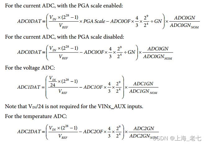
For these equations, note the following:
- 29/24 is used to transform ADCxOF format (24-bit data) to ADCxDAT format (32-bit data).
- 4/3 is used to scale ADCxOF data back to actual data, because ADCxOF is 0.75 of the actual offset.
- ADCxGNNOM = 0x5555.
- ADC works in twos complement mode.
对于这些公式,请注意以下事项:
29/24 用于将 ADCxOF 格式(24 位数据)转换为 ADCxDAT 格式(32 位数据)。
4/3 用于将 ADCxOF 数据缩放回实际数据,因为 ADCxOF 是实际偏移量的 0.75。
ADCxGNNOM = 0x5555。
ADC 工作在二进制补码模式。
6.3.4 Calibration Modes模数转换器标定模式
6.3.4.1 Self Offset Calibration: ADCMDE = 0x4自偏置校准
In this mode, an offset calibration is performed on any enabled ADC using an internally generated 0 V signal. The calibration is carried out at the user programmed ADC settings; therefore, as with a normal single ADC conversion, it takes two to three ADC conversion cycles before a fully settled calibration result is ready. The calibration result is automatically written to the ADC data register of the respective ADC; the user must transfer the results to the ADCxOF register. After a device reset, the ADCxOF register is reloaded with the factory calibration value.
在此模式下,使用内部生成的0 V信号对任何使能的ADC执行失调校准。进行校准在用户编程的ADC设置下;因此,与正常的单ADC转换一样,需要2到3个ADC转换在完全稳定的校准结果准备就绪之前循环。校准结果自动写入各自的 ADC;用户必须将结果传输到ADCxOF寄存器。器件复位后,ADCxOF 寄存器重新加载出厂校准值。
6.3.4.2 Self Gain Calibration: ADCMDE = 0x5自增益校准
In this mode, a gain calibration against selected reference voltage is performed on all enabled ADCs. A gain calibration is a two-stage process and takes twice the time of an offset calibration. The calibration result is automatically written to the ADC data register of the respective ADC; the user must transfer the results to the gain register. The internal full-scale calibration does not work for gain settings greater than 1. After a device reset, the ADC gain register is reloaded with the factory calibration value.
在此模式下,在所有使能的ADC上针对所选基准电压执行增益校准。增益校准为两级处理并花费两倍的偏移校准时间。校准结果自动写入各自的 ADC;用户必须将结果传输到增益寄存器。内部满量程校准不适用于增益设置大于 1。器件复位后,ADC增益寄存器将重新加载出厂校准值。
6.3.4.3 System Zero-Scale Calibration: ADCMDE = 0x6系统零刻度校准
In this mode, a zero-scale calibration is performed on enabled ADC channels against an external zero-scale voltage driven at the ADC input pins. Usually, the selected channel is shorted externally. The calibration result is automatically written to the ADC data register of the respective ADC. The user must transfer the results to the offset register.
在此模式下,根据ADC驱动的外部零电平电压,在使能的ADC通道上执行零电平校准输入引脚。通常,所选通道在外部短路。校准结果自动写入相应的 ADC。用户必须将结果传输到偏移寄存器。
6.3.4.4 System Full-Scale Calibration: ADCMDE = 0x7系统满量程校准
In this mode, a full-scale calibration is performed using the enabled ADC channels against an external full-scale voltage driven at the ADC input pins. The ADC gain register is updated after a full-scale calibration sequence. After a device reset, the ADC gain register is reloaded with the factory calibration value.
在此模式下,使用使能的ADC通道针对在ADC 输入引脚。ADC增益寄存器在满量程校准序列后更新。器件复位后,ADC增益寄存器为已重新加载出厂校准值。
Note that, when the ADC is delivering samples at a rate of 1/fADC, take care when modifying the ADCxGN and ADCxOF registers to avoid writing to them while the ADC is reading these registers. Ensure that the ADC is in idle mode when modifying the ADCxGN and ADCxOF registers, or ensure that the ADCxGN and ADCxOF registers are modified between the start of the conversion to 1/fADC − 344 clock cycles (16 MHz).
It is strongly recommended that ADC calibration is initiated at the lowest ADC update rate possible (high SF value in ADCFLT) to minimize the impact of ADC noise during calibration. Do not use calibration registers for coarse scaling of input ranges.
请注意,当ADC以1/fADC的速率提供样本时,对ADCxGN和ADCxOF寄存器修改时要小心,避免在ADC读取这些寄存器时写入它们。确保在修改ADCxGN时ADC处于空闲模式,并且ADCxOF 寄存器,或确保在转换开始转换为 1/fADC − 344 之间修改 ADCxGN 和 ADCxOF 寄存器时钟周期 (16 MHz)。
强烈建议以尽可能低的ADC更新速率(ADCFLT中的高SF值)启动ADC校准,以将校准期间ADC噪声的影响降至最低。不要使用校准寄存器对输入范围进行粗略缩放
6.4 ADC SINC3 DIGITAL FILTER RESPONSE模数转换器sinc3数字滤波器响应
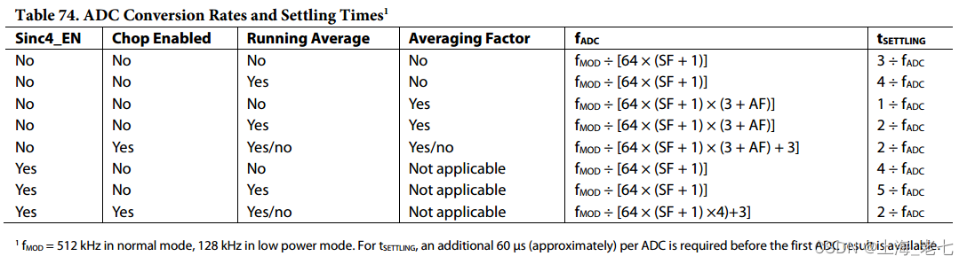
The overall frequency response on all ADuCM330/ADuCM331 ADCs is dominated by the low-pass filter response of the on-chip, sinc3 and sinc4 digital filters. The sinc3 and sinc4 filters are used to decimate the ADC Σ-Δ modulator output data bit stream and to generate a valid 20-bit data result. The digital filter response is identical for both ADCs and is configured via the 20-bit ADC filter (ADCFLT) register.
This register determines the overall throughput rate of the ADCs. The noise resolution of the ADCs is determined by the programmed ADC throughput rate. In the case of the current ADC, the noise resolution is determined by the throughput rate and selected gain.
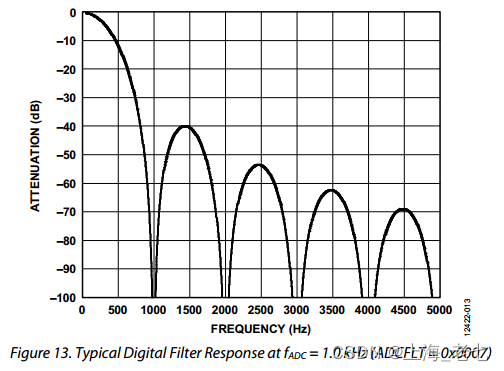
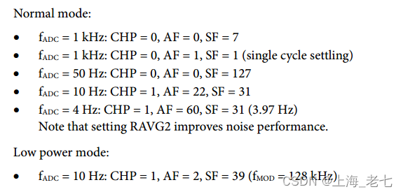
The overall frequency response and the ADC throughput is dominated by the configuration of the sinc3 filter decimation factor (SF) bits (ADCFLT[6:0]) and the averaging factor (AF) bits (ADCFLT[13:8]). Due to limitations on the digital filter internal data path, there are some limitations on the allowable combinations of SF and AF that can be used to generate a required ADC output rate. This restriction limits the minimum ADC update in normal power mode to 4 Hz (chop on, AF = 60, SF = 31). The calculation of the ADC throughput rate is detailed in Table 88.
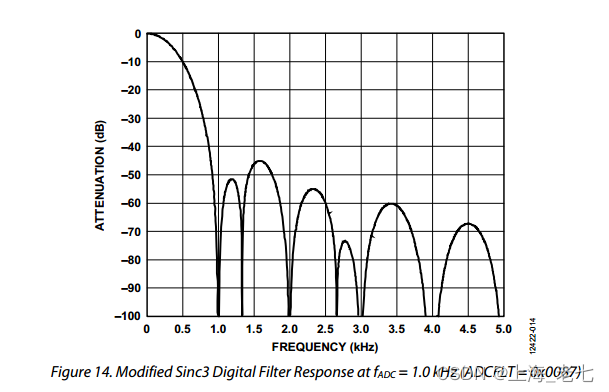
By default, ADCFLT = 0x0007 configures the ADCs for a throughput rate of 1.0 kHz with all other filtering options (chop, running average, averaging factor, and sinc3 modify) disabled. A typical filter response based on this default configuration is shown in Figure 13.
所有ADuCM330/ADuCM331 ADC的整体频率响应主要由片内sinc3的低通滤波器和 SinC4 数字滤波器响应主导。sinc3和sinc4滤波器用于抽取ADC Σ-Δ调制器输出数据位流,并生成有效的 20 位数据结果。两个ADC的数字滤波器响应相同,并通过20位ADC滤波器(ADCFLT)寄存器进行配置。该寄存器决定了ADC的总体吞吐速率。ADC的噪声分辨率由编程决定ADC 吞吐速率。对于电流ADC,噪声分辨率由吞吐速率和所选增益决定。
整体频率响应和ADC吞吐量主要由sinc3滤波器抽取因子(SF)位的配置决定(ADCFLT[6:0])和平均因子(AF)位(ADCFLT[13:8])。由于数字滤波器内部数据路径的限制,存在SF和AF的允许组合的一些限制,可用于产生所需的ADC输出速率。此限制将正常功率模式下的最小 ADC 更新限制为 4 Hz(斩波,AF = 60,SF = 31)。ADC 吞吐量的计算速率详见表88。
默认情况下,ADCFLT = 0x0007 使用所有其他滤波选项(斩波、运行平均值、平均因子和 sinc3 修改)禁用。基于此默认配置的典型滤波器响应如图13所示。
An additional sinc3 modify bit (ADCFLT[7]) is also available in the ADCFLT register. This bit is set by user code to modify the standard sinc3 frequency response, increasing the filter stop-band rejection by approximately 5 dB. This modification is achieved by inserting a second notch (NOTCH2) at
ADCFLT寄存器中还有一个额外的sinc3修改位(ADCFLT[7])。该位由用户代码设置,以修改标准sinc3频率响应,将滤波器阻带抑制提高约5 dB。此修改基于公式:
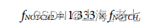
where fNOTCH is the location of the first notch in the response.
其中 fNOTCH 是响应中第一个缺口的位置。
There is a slight increase in ADC noise if the sinc3 modify bit is active. Figure 14 shows the modified 1 kHz filter response when the sinc3 modify bit is active. The new notch is visible at 1.33 kHz, as is the improvement in stop-band rejection when compared to the standard 1 kHz response.
如果sinc3修改位处于活动状态,ADC噪声会略有增加。图14显示了sinc3修改位处于活动状态时的修改后的1 kHz滤波器响应。新的陷波在1.33 kHz时可见,与标准1 kHz响应相比,阻带抑制也有所改善。
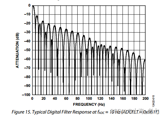
At very low throughput rates, the chop bit in the ADCFLT register can be enabled to minimize offset errors and, more importantly,temperature drift in the ADC offset error.
There are two primary variables (sinc3 decimation factor and averaging factor) available to allow the user to select an optimum filter response, trading off filter bandwidth against ADC noise. For example, with the chop bit (ADCFLT[15]) set to 1, increasing the SF value (ADCFLT[6:0]) to 0x1F (31 decimal) and selecting an AF value (ADCFLT[13:8]) of 0x16 (22 decimal) results in an ADC throughput of 10 Hz. The frequency response in this case is shown in Figure 15.
在非常低的吞吐速率下,可以启用ADCFLT寄存器中的斩波位,以最小化失调误差,更重要的是,使ADC失调误差中的温度漂移最小化。
有两个主要变量(sinc3抽取因子和平均因子)允许用户选择最佳滤波器响应,权衡滤波器带宽与ADC噪声。例如,将斩波位 (ADCFLT[15]) 设置为 1,将 SF 值 (ADCFLT[6:0]) 增加到 0x1F(31 十进制),并选择 0x16 (22 十进制)的 AF 值 (ADCFLT[13:8]) 会导致 ADC 吞吐量为 10 Hz。本例中的频率响应如图15所示。
In ADC low power mode, the Σ-Δ ADC modulator clock is no longer driven at 512 kHz but at 128 kHz. Subsequently, for the same ADCFLT configurations in normal mode, all filter values must be scaled by a factor of approximately four.
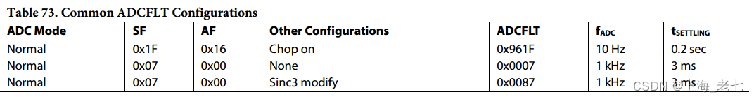
In general, it is possible to program different values of SF and AF in the ADCFLT register and achieve the same ADC update rate. In practical terms, the trade off with any value of ADCFLT is frequency response versus ADC noise. For optimum filter response and ADC noise when using combinations of SF and AF, the best practice is to choose an SF in the range of 16 decimal to 40 decimal, or 0x10 to 0x28, and increasing the AF value to achieve the required ADC throughput. Table 73 shows some common ADCFLT configurations.
在ADC低功耗模式下,Σ-Δ ADC调制器时钟不再以512 kHz驱动,而是以128 kHz驱动。随后,对于正常模式下的相同ADCFLT配置,所有滤波器值必须按大约四倍的调整。
通常,可以在ADCFLT寄存器中对SF和AF的不同值进行编程,并实现相同的ADC更新速率。实际上,任何ADCFLT值的权衡都是频率响应与ADC噪声。为了在使用SF和AF组合时获得最佳滤波器响应和ADC噪声,最佳做法是选择16位小数到40位小数或0x10到0x28范围内的SF,并增加AF值以实现所需的ADC吞吐量。表73显示了一些常见的ADCFLT配置。
6.5 DIGITAL FILTER OPTIONS模数转换器数字滤波器选项
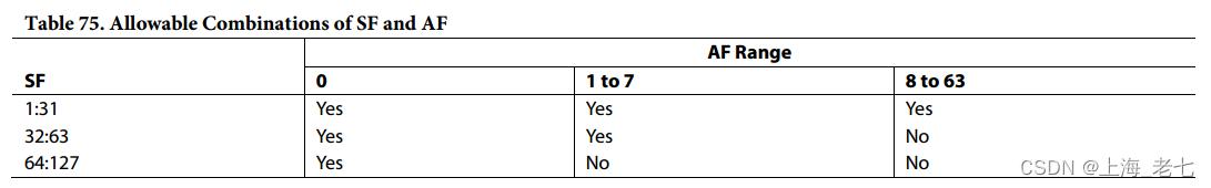
The combination limit shown in Table 75 is only for sinc3 mode.
The ADuCM330/ADuCM331 also incorporate a sinc4 digital filtering option. The sinc4 filter offers reduced noise, particularly at high (>2 kHz) output rates, and is recommended for these applications. Contact Analog Devices for a spreadsheet application showing the ADC frequency response for both sinc3 and sinc4 filtering options.
For sinc4 mode:
• AF is not applicable and always forced to be zero.
• SF must be no greater than 0x0E. If SF is set to greater than 0x0E in sinc4 mode, it is automatically forced to 0x0E.
表 75 中所示的组合限值仅适用于 sinc3 模式。
ADuCM330/ADuCM331还集成了sinc4数字滤波选项。sinc4滤波器可降低噪声,特别是在高(>2 kHz)输出速率下,推荐用于这些应用。联系ADI公司获取电子表格应用,显示sinc3和sinc4滤波选项的ADC频率响应。
对于 sinc4 模式:
• AF 不适用,并且始终强制为零。
• SF 不得大于 0x0E。如果在 sinc4 模式下将 SF 设置为大于 0x0E,则会自动强制0x0E。
6.6 ADC CONFIGURATION模数转换器配置
Fast Temperature Conversion Mode
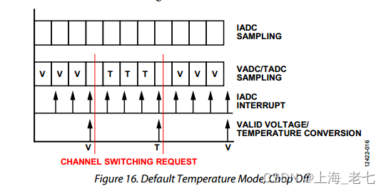
The battery temperature can be derived through the on-chip temperature sensor. By default, the time to a first valid (fully settled) result after switching the ADC input from the voltage to the temperature channel or from the temperature to the voltage channel is three ADC conversion cycles with chop mode turned off, as shown in Figure 16.
快速温度转换模式
电池温度可以通过片上温度传感器得出。默认情况下,将ADC输入从电压通道切换到温度通道或从温度通道切换到电压通道后,获得第一个有效(完全建立)结果的时间是三个ADC转换周期,斩波模式关闭,如图16所示。
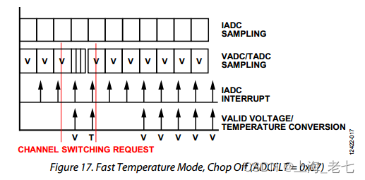
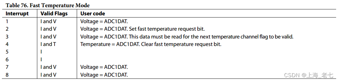
A fast mode is provided on the temperature channel to minimize the switching delay between voltage conversion and temperature conversions, as shown in Figure 17 and in Table 76.
A request for a fast temperature conversion is executed with a delay of one ADC conversion. The fast temperature mode must be cleared after the temperature measurement is available and before a new temperature request.
温度通道上提供快速模式,以最小化电压转换和温度转换之间的开关延迟,如图17和表76所示。
执行快速温度转换请求时延迟一个ADC转换。在温度测量可用之后和新的温度请求之前,必须清除快速温度模式。
The fast temperature option cannot be used on the first conversion after ADC power-on. The option can only be set after at least the first ADC interrupt. Waiting for a valid ADC result is not necessary. When using the fast temperature mode, ensure that SF ≥ 1. In addition, a conversion rate of 1 ms is recommended in this mode of operation, to ensure that the fast result occurs simultaneously with the current channel result.
When changing the ADCs configuration by writing to ADCMDE, ADC0CON or ADCFLT, the fast temperature bit must also be cleared to ensure correct operation. This condition is similar to a first conversion after ADC power-on.
快速温度选项不能用于ADC上电后的第一次转换。该选项只能在至少第一个ADC中断后设置。无需等待有效的ADC结果。使用快速升温模式时,请确保顺丰≥ 1。此外,在这种工作模式下,建议转换速率为1 ms,以确保快速结果与当前通道结果同时出现。
通过写入ADCMDE、ADC0CON或ADCFLT来更改ADC配置时,还必须清除快速温度位以确保正确操作。这种情况类似于ADC上电后的第一次转换。
6.7 IADC DIAGNOSTICS电流模数转换器诊断
The ADuCM330/ADuCM331 feature the capability to detect open circuit conditions on the application board. This detection is accomplished using the two current sources on IIN+ and IIN−; these sources are controlled via ADC0CON[13:12].
Note that these current sources have a tolerance of ±10%.
ADuCM330/ADuCM331具有检测应用板上开路条件的功能。该检测是使用 IIN+ 和 IIN− 上的两个电流源完成的;这些来源通过ADC0CON[13:12]进行控制。
请注意,这些电流源的容差为 ±10%。
6.8 OTHER ADC SUPPORT CIRCUITS其他模数转换器支持电路
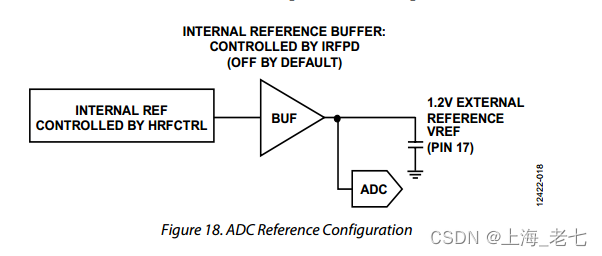
6.8.1 Internal/External 1.2V Voltage Reference内部/外部1.2V基准电压源
It is possible to apply an external reference to the ADuCM330/ADuCM331. To use an external reference, the following steps are required:
• Power down the internal reference buffer by setting IRFPD = 0x01. This is also the default state.
• Apply an external reference to VREF (1.2 V).
The ADCs operate as normal
**可以对ADuCM330/ADuCM331应用外部基准电压源。要使用外部基准电压源,需要执行以下步骤:
• 通过设置 IRFPD = 0x01 来关断内部基准电压缓冲器。这也是默认状态。
• 将外部基准应用于 VREF (1.2 V)。
模数转换器正常工作 **
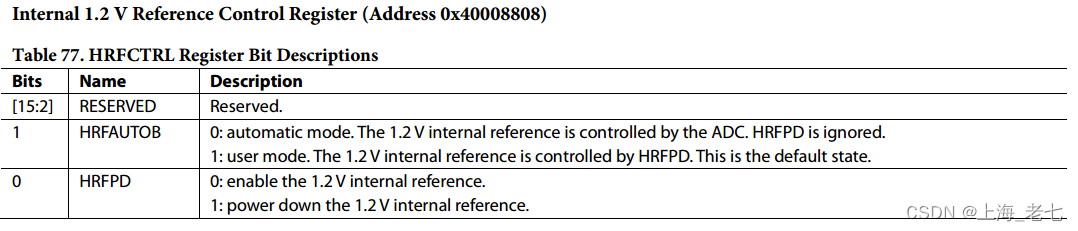
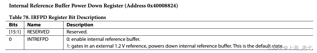
Note the following:
• If using an external reference, the reference buffer must be disabled via the IRFPD register. However, the internal 1.2 V reference must be kept enabled, because it is still required internally for correct functionality.
• When using the internal 1.2 V reference for the ADCs, both the reference and the buffer must be enabled.
• When using the internal 1.2 V reference for the ADCs, ensure that the reference buffer is enabled or disabled according to ADCxCON[19].
• Before entering hibernate mode, follow the recommended ADC power-down sequence (see the Power-Down Mode section).
请注意以下几点:
• 如果使用外部基准,则必须通过 IRFPD 寄存器禁用基准电压缓冲器。但是,内部1.2 V基准电压源必须保持启用状态,因为内部仍然需要它才能实现正确的功能。
• ADC使用内部1.2 V基准电压源时,必须同时使能基准电压源和缓冲器。
• 对ADC使用内部1.2 V基准电压源时,请确保根据ADCxCON[19]启用或禁用基准电压缓冲器。
• 在进入休眠模式之前,请遵循推荐的 ADC 关断顺序(请参阅省电模式部分)。
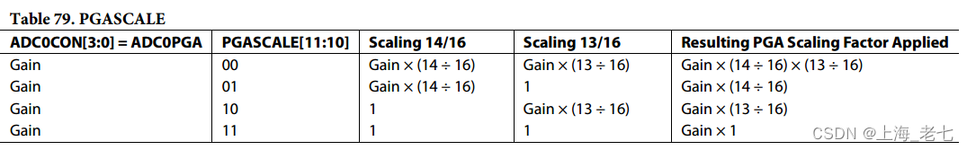
6.8.2 Programmable Gain Amplifier可编程增益放大器
The primary ADC (current ADC) incorporates an on-chip, programmable gain amplifier (PGA). The gain is controlled by the ADC0CON register. The PGA allows signals of very small amplitude to be gained up while still maintaining low noise performance.
Internally, the PGA requires its output range to be limited to <±1 V while still allowing a 1.2 V reference to be used.
To accommodate this requirement, there are two bits at ADC0CON[11:10] named PGASCALE. Clearing these bits (default state) activates a 13/16 × 14/16 scaling factor and maintains compatibility with gain ranges from previous IBS generations.
If the PGASCALE bits are both set to 1, ensure that the input to the PGA does not exceed 1 V/gain.
主ADC(电流ADC)集成了一个片内可编程增益放大器(PGA)。增益由ADC0CON寄存器控制。PGA允许获得非常小幅度的信号,同时仍保持低噪声性能。
在内部,PGA要求其输出范围限制在<±1 V,同时仍允许使用1.2 V基准电压源。
为了满足此要求,ADC0CON[11:10] 有两个位名为 PGASCALE。清除这些位(默认状态)将激活 13/16 × 14/16 比例因子,并保持与前几代 IBS 增益范围的兼容性。
如果PGASCALE位都设置为1,请确保PGA的输入不超过1 V/增益。
6.8.3 ADC Comparator and Accumulator模数转换器比较器和累加器
The current ADC result can be compared to a preset threshold level (ADC0TH) configured via the ADCCFG register. An interrupt is generated if the absolute (sign independent) value of the ADC result is greater than the preprogrammed comparator threshold level. An ADC interrupt is also generated when the threshold counter reaches a preset value (ADC0RCL).
Finally, a 32-bit accumulator (ADC0ACC) contains the result of multiple primary conversions. User code can read the accumulated value directly (ADC0ACC) without any further software processing.
可以将电流ADC结果与通过ADCCFG寄存器配置的预设阈值电平(ADC0TH)进行比较。如果ADC结果的绝对(与符号无关)值大于预编程比较器阈值电平,则会产生中断。当阈值计数器达到预设值(ADC0RCL)时,也会生成ADC中断。
最后,32位累加器(ADC0ACC)包含多次主转换的结果。用户代码可以直接读取累积值(ADC0ACC),而无需任何进一步的软件处理。
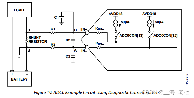
6.8.4 Diagnostic Current Sources诊断电流源
For diagnostic purposes, both ADCs of the ADuCM330/ADuCM331 incorporate 50 µA constant current sources. These current sources can be controlled by the appropriate bits in the ADCxCON registers. For all current input channels (IIN+/IIN− and IIN+_AUX/IIN−_AUX),independent current sources are available.
For the implementation of diagnostic functions in the application, the user must take into account the internal present RIN+/RIN− (see Figure 19). The resistors are approximately in the range of 1.8 kΩ ± 10%. In addition, the 50 µA current sources are typically ±10% accurate.
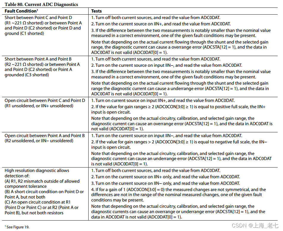
Therefore, with the external recommended filter resistors, shown as R1 and R2 with a value of 221 Ω ± 1%, the minimum and maximum voltage change after switching on such a diagnostic current is typically in the range from 82 mV to 121 mV. Table 80 shows some possible fault conditions and possible tests for error detection. To conduct these tests, an appropriate gain range must be selected.
Note that for higher gain ranges (gain ≥ 8, ADC0CON[3:0] ≥ 3), in most cases, the diagnostic currents cause an underrange or overrange error status (ADCSTA[12] = 1 and ADC0DAT[0] = 1).
出于诊断目的,ADuCM330/ADuCM331的两个ADC均集成了50 μA恒流源。这些电流源可由ADCxCON寄存器中的相应位控制。对于所有电流输入通道(IIN+/IIN− 和 IIN+_AUX/IIN−_AUX),均提供独立的电流源。
为了在应用中实现诊断功能,用户必须考虑内部存在的RIN+/RIN−(参见图19)。电阻大约在1.8 kΩ±10%范围内。此外,50 μA电流源的精度通常为±10%。
因此,使用外部推荐的滤波电阻(显示为R1和R2,值为221 Ω ± 1%),打开此类诊断电流后的最小和最大电压变化通常在82 mV至121 mV范围内。表 80 显示了一些可能的故障条件和可能的错误检测测试。要进行这些测试,必须选择合适的增益范围。
请注意,对于更高的增益范围(增益≥8、ADC0CON[3:0] ≥ 3),在大多数情况下,诊断电流会导致欠量程或超量程误差状态(ADCSTA[12] = 1 和 ADC0DAT[0] = 1)。
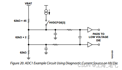
On the VBAT input channel, constant current sources are available on the HV die and the LV die. For the VBAT channel, the primary measurement channel, it is recommended to use the current source on the HV die for diagnostics, as shown in Figure 20. If the current source on the HV die in HVDCFG0[3] is enabled, a typical voltage of 160 mV ± 5% is added to the actual voltage measured from VBAT.
在VBAT输入通道上,高压芯片和低压芯片上提供恒流源。对于VBAT通道(主测量通道),建议使用高压芯片上的电流源进行诊断,如图20所示。如果使能HVDCFG0[3]中高压芯片上的电流源,则在VBAT测量的实际电压的基础上增加160 mV±5%的典型电压。
6.9 ADC CHOPPING模数转换器斩波
The ADCs on the ADuCM330/ADuCM331 implement a chopping scheme whereby the ADC repeatedly reverses its inputs. Therefore,the decimated digital output values from the sinc3 or sinc4 filter have a positive and negative offset term associated with them. This results in the ADC including a final summing stage that sums and averages each value from the filter with previous filter output values.
This new value is then sent to the ADC data MMR. This chopping scheme results in excellent dc offset and offset drift specifications and is extremely beneficial in applications where drift and noise rejection are required. Chopping is not active by default, meaning there is an offset error. Chopping also affects settling time, as shown in Table 74.
ADuCM330/ADuCM331上的ADC采用斩波方案,ADC反复反转其输入。因此,sinc3或sinc4滤波器抽取的数字输出值具有与之相关的正负偏移项。这导致ADC包括一个最终求和阶段,该阶段将滤波器的每个值与先前的滤波器输出值相加并求平均值。
然后将此新值发送到ADC数据MMR。这种斩波方案可实现出色的直流失调和失调漂移规格,在需要漂移和噪声抑制的应用中极为有利。默认情况下,斩波不处于活动状态,这意味着存在偏移误差。斩波也会影响建立时间,如表74所示。
6.10ADC REGISTERS模数转换器寄存器
6.10.1 ADC Status Register (Table 83)模数转换器状态寄存器
The various enabled ADC interrupts sources are OR’ed to produce a single ADC interrupt to the ARM core. The software then interrogates the ADCSTA MMR to determine the source of the interrupt. The ADC0RDY and ADC1RDY bits are set simultaneously if both the IADC and VADC are enabled. If a temperature channel is selected, the ADC1RDY bit is not set, but the ADC2RDY bit is set.
All the RDY bits are cleared by a read of the ADC0DAT MMR. Writing to the ADC0CON register also clears all the ADCSTA bits.
A change in the ADC1CON register only clears ADCSTA[1]. This bit is also cleared by reading the ADC1DAT register.
If the IADC is not enabled, all the RDY bits are cleared by a read of the ADC1DAT MMR. Therefore, software routines that need to access current/voltage data that is guaranteed synchronously sampled must read the ADC1DAT register before reading the ADC0DAT register;otherwise, a read of the ADC0DAT register clears the RDY1 flag, allowing the possibility of the ADC1DAT register being overwritten by new data before it is read.
各种使能的 ADC 中断源经过 OR 运算,以产生到 ARM 内核的单个 ADC 中断。然后,软件询问ADCSTA MMR以确定中断源。如果同时启用了电流ADC和电压ADC,则同时设置ADC0RDY位和ADC1RDY位。如果选择温度通道,则不设置ADC1RDY位,但设置ADC2RDY位。
所有RDY位都通过读取ADC0DAT MMR清除。写入ADC0CON寄存器也会清除所有ADCSTA位。
ADC1CON寄存器中的更改仅清除ADCSTA[1]。该位也通过读取ADC1DAT寄存器来清除。
如果未启用电流ADC,则通过读取ADC1DAT MMR 清除所有 RDY 位。因此,如果软件例程需要访问保证同步采样的电流/电压数据,则必须在读取ADC0DAT寄存器之前读取ADC1DAT寄存器;否则,读取ADC0DAT寄存器会清除RDY1标志,从而允许ADC1DAT寄存器在读取之前被新数据覆盖。
Summary of How the Status Register Flags Are Reset
• The ADCxERR flags are set or cleared every time new data is written into the appropriate ADCxDAT MMR, setting the ADCxRDY bits.The flags are not cleared by a read of the ADCxDAT MMRs.
• Comparator/counter interrupts are cleared if the comparator/counter is disabled.
• The ADCxRDY bits are automatically cleared by the ADC if the ADC configuration is changed.
• The ADCxRDY flags are cleared by a read of the ADC0DAT register or a read of the ADC1DAT register if the IADC is not active.
All other interrupts and flags are also cleared if the ADC configuration is changed.
如何重置状态寄存器标志的摘要
• 每次将新数据写入适当的ADCxDAT MMR时,都会设置或清除ADCxERR标志,从而设置ADCxRDY位。读取ADCxDAT MMR不会清除这些标志。
• 如果禁用比较器/计数器,则清除比较器/计数器中断。
• 如果ADC配置发生变化,ADC会自动清除ADCxRDY位。
• 如果电流ADC没有激活,则读取ADC0DAT寄存器或读取ADC1DAT寄存器会清除ADCxRDY标志。
如果ADC配置发生更改,所有其他中断和标志也会被清除。
6.10.2 ADC Mask Register (Table 84)模数转换器屏蔽寄存器
This MMR allows the ADC interrupt sources in the ADCSTA register to be individually masked. The bit positions are the same as the lower five bits of ADCSTA. If a bit is set to 1, the interrupt is enabled. The default value is 0x00, that is, all ADC interrupts are inactive.
The ADCMSKI register is used to enable the lower bits of the ADCSTA register to generate an interrupt.
该MMR允许对ADCSTA寄存器中的ADC中断源进行单独屏蔽。位位置与ADCSTA的下五位相同。如果位设置为 1,则启用中断。默认值为 0x00,即所有 ADC 中断都处于非活动状态。
ADCMSKI寄存器用于使能ADCSTA寄存器的低位产生中断。
6.10.3 ADC Mode Register (Table 85)模数转换器模式寄存器
A write to the ADCMDE register immediately resets each active ADC, including the ADCxRDY bits and other ADCSTA flags. The full digital filter settling time must elapse before the first result with the new MMR programmed configuration is available. The one exception to this condition is that an interrupt can be provided before the filter is settled if the always interrupt mode bit is set.
The results of the calibrations are written into the ADCxDAT registers. The user must copy the calibration results from the ADCxDAT registers into ADCxOF/ADCxGN.
写入ADCMDE寄存器会立即复位每个活动ADC,包括ADCxRDY位和其他ADCSTA标志。完整的数字滤波器建立时间必须经过,然后才能获得具有新MMR编程配置的第一个结果。这种情况的一个例外是,如果设置了始终中断模式位,则可以在滤波器建立之前提供中断。
校准结果写入ADCxDAT寄存器。用户必须将校准结果从ADCxDAT寄存器复制到ADCxOF/ADCxGN中。
6.10.4 ADC Control Register: ADC0CON (Table 86)模数转换器控制寄存器ADC0CON
A write to the ADC0CON register resets the IADC and other enabled ADCs. The full digital filter settling time must elapse before a result is available.
If the two ADCs are being reconfigured at the same time, ADC0CON must be written last to ensure that the voltage/temperature channel restarts converting at the same time as the current channel. However, if the voltage/temperature ADCs are powered down, there is a power-up delay before the voltage/temperature channel can start converting, which can mean that the IADC has started converting, and the voltage/temperature channel cannot start its conversion until the IADC has provided an output.
写入ADC0CON寄存器可重置电流ADC和其他已启用的ADC。完整的数字滤波器建立时间必须经过,才能获得结果。
如果两个ADC同时重新配置,则必须最后写入ADC0CON,以确保电压/温度通道与电流通道同时重新开始转换。但是,如果电压/温度ADC断电,则在电压/温度通道开始转换之前存在上电延迟,这可能意味着IADC已开始转换,并且在IADC提供输出之前,电压/温度通道无法开始转换。
6.10.5 ADC Control Register: ADC1CON (Table 87)模数转换器控制寄存器ADC1CON
A write to the ADC1CON register resets the VADC/TADC. The VADC/TADC restarts at an appropriate time so that its outputs are synchronous with the IADC, that is, the IADC is not reset by a change in the VADC/TADC configuration. The full VADC/TADC digital filter settling time must elapse before a voltage or temperature result is available.
写入ADC1CON寄存器可重置电压ADC/温度ADC。电压ADC/温度ADC在适当时候重新启动,以便其产出与电流ADC同步,也就是说,改变电压ADC/温度ADC配置不会使电流ADC复位。完整的电压ADC/温度ADC数字滤波器建立时间必须经过,才能获得电压或温度结果。
6.10.6 ADC Filter Register (Table 88)模数转换器滤波器寄存器
The ADCFLT register controls the output speed of the ADC, which influences the noise of the ADC. A write to ADCFLT resets the corresponding ADC.
ADCFLT寄存器控制ADC的输出速度,这会影响ADC的噪声。写入ADCFLT会重置相应的ADC。
6.10.7 ADC Configuration Registers (Table 89)模数转换器配置寄存器
A write to the ADCCFG register does not reset the ADC.
If the overrange or comparator interrupts are set, the interrupt can be disabled by one of the following methods:
• Clearing the interrupt mask in ADCSTA
• Disabling comparator
• Reconfiguring the ADC
Note that the comparator must be disabled for at least one full conversion period to ensure that the comparator interrupt is reset. Also,the interrupt mask in ADCMSKI (ADCMSKI[4]) must be cleared to prevent unwanted interrupts during this period.
The result counter does not produce an interrupt of its own, but only gates the ADCxRDY interrupts.
If the result counter and the always interrupt mode are both active, the ADC operation is undefined.
写入ADCCFG寄存器不会重置ADC。
如果设置了超量程或比较器中断,则可以通过以下方法之一禁用中断:
• 清除ADCSTA中的中断屏蔽位
• 禁用比较器
• 重新配置 ADC
注意,必须禁用比较器至少一个完整转换周期,以确保比较器中断复位。此外,必须清除ADCMSKI(ADCMSKI[4])中的中断屏蔽位,以防止在此期间出现不必要的中断。
结果计数器本身不产生中断,而只对ADCxRDY中断进行门控。
如果结果计数器和始终中断模式都处于活动状态,则 ADC 操作未定义。
6.10.8 ADC Data Register (Table 90 and Table 91)模数转换器数据寄存器
Figure 21 shows the formatting of the 32-bit ADC0DAT register according to the gain setting selected. The ADC1DAT register does not have this shifting of data as there is no gain control on the voltage/temperature channel.
Only the relevant data bits in the ADC0DAT register are set depending on the gain setting. This means that no software adjustment to the ADC0DAT result is required for different gain settings. The result is automatically adjusted internally based on the gain setting.
图21显示了根据所选增益设置对32位ADC0DAT寄存器的格式化。ADC1DAT寄存器没有这种数据偏移,因为电压/温度通道上没有增益控制。
只有ADC0DAT寄存器中的相关数据位会根据增益设置进行设置。这意味着对于不同的增益设置,无需对ADC0DAT结果进行软件调整。ADC0DAT结果会根据增益设置在内部自动调整。
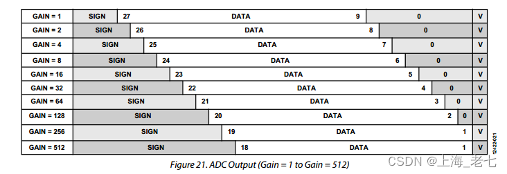
The data format of ADCxDAT is twos complement or unipolar, based on the ADCxCODE bits in the ADCxCON registers.
The ADC0DAT register output equals a useful signal range of bits from 18 to 3 at a gain of 512 and noise from Bit 2 to Bit 1.
ADCxDAT[0] indicates if valid data is available. If ADCxDAT[0] = 1, the data is invalid. If ADCxDAT[0] = 0, the data is valid.
ADCxDAT的数据格式为二进制补码或单极性,基于ADCxCON寄存器中的ADCxCODE位。
ADC0DAT寄存器输出等于增益为512时18至3位的有用信号范围,以及从位2到位1的噪声。
ADCxDAT[0] 指示有效数据是否可用。如果 ADCxDAT[0] = 1,则数据无效。如果 ADCxDAT[0] = 0,则数据有效。
For improved accuracy, adjust the gain to match the expected signal with the correct input range. This can be seen in Figure 21. For example, when measuring a small signal at a gain of 1, mostly noise is being measured. At a gain of 512, there are a number of bits with more useful data to give an accurate result. Note that for faster update rates, the noise increases.
为了提高精度,请调整增益以将预期信号与正确的输入范围相匹配。如图 21 所示。例如,当测量增益为1的小信号时,主要测量的是噪声。增益为512时,有许多位具有更有用的数据,以提供准确的结果。请注意,更新速率越快,噪音会增加。
Reading the ADC0DAT register clears any active RDY flags.
The ADC cannot write new data into the ADCxDAT register if the relevant ADCxRDY bits are set. This does not apply if the core is off;when the core is off, the ADCxDAT register contains the most recent ADC data.
The data registers are written simultaneously if all ADCs are active, and the ADCxRDY bits are set when the ADCxDAT MMRs are written.
读取ADC0DAT寄存器将清除所有活动的 RDY 标志。
如果设置了相关的ADCxRDY位,ADC无法将新数据写入ADCxDAT寄存器。这不适用于内核关闭的情况;当内核关闭时,ADCxDAT寄存器包含最新的ADC数据。
如果所有ADC都处于激活状态,则会同时写入数据寄存器,并在写入ADCxDAT MMR时设置ADCxRDY位。
If the configuration of the ADC1 is changed in the middle of a conversion, a number of ADC results occur where data is only written into the ADC0DAT data.
If the ADCxRDY bit is low, there is no guarantee that the ADCxDAT MMRs are stable if read.
If the ADC0 result counter is active, the data register (ADC0DAT) is not updated until the ADC0RDY bit is set, that is, when the ADC0RCV counter reaches the programmed limit (ADC0RCL). This condition does not hold if the core is off, in which case the ADC0DAT MMR(s) contain the most recent ADC result(s) when the core wakes up.
如果在转换过程中更改ADC1的配置,则会出现许多ADC结果,其中数据仅写入ADC0DAT数据。
如果ADCxRDY位为低电平,则无法保证ADCxDAT MMR在读取时稳定。
如果ADC0结果计数器处于活动状态,则在设置ADC0RDY位之前,即当ADC0RCV计数器达到编程限值(ADC0RCL)之前,数据寄存器(ADC0DAT)不会更新。如果内核关闭,则此条件不成立,在这种情况下,当内核唤醒时,ADC0DAT MMR 包含最新的 ADC 结果。
In calibration mode, the result of the calibration is stored in the ADCxDAT register. The user must transfer the result to the ADCxGN or ADCxOF register.
在校准模式下,校准结果存储在ADCxDAT寄存器中。用户必须将结果传输到ADCxGN或ADCxOF寄存器。
6.10.9 ADC Calibration Registers模数转换器校准寄存器
In gain calibration mode, the result of the calibration is stored in ADCxDAT[15:0]. The user must transfer the result to ADCxGN[15:0].
In offset calibration mode, the result of the calibration is stored in ADCxDAT[24:0]. The user must transfer the result to ADCxOF[23:0].
在增益校准模式下,校准结果存储在ADCxDAT[15:0]中。用户必须将结果传输到ADCxGN[15:0]。
在偏移校准模式下,校准结果存储在ADCxDAT[24:0]中。用户必须将结果传输到 ADCxOF[23:0]。
6.10.10 ADC Offset Registers (Table 92, Table 93, and Table 94)模数转换器偏移寄存器
The offset registers are in signed twos complement form. A code of 0000 means subtract 0 offset. This form does not change to unipolar if the ADCxCODE bit in the ADCxCON register is set.
偏移寄存器采用带符号二进制补码形式。代码 0000 表示减去 0 偏移量。如果设置了ADCxCON寄存器中的ADCxCODE位,则此形式不会变为单极性。
6.10.10.1 ADC0OF
If performing a manual offset calibration with an external shorted input, the ADC0DAT[31:0] result can be transferred to the ADC0OF register using the following formula:
如果使用外部短路输入执行手动偏移校准,则可以使用以下公式将ADC0DAT[31:0]结果传输到ADC0OF寄存器:

6.10.10.2 ADC1OF
If performing a manual offset calibration, the ADC1DAT[31:0] result can be transferred to the ADC1OF register using the following formula:
如果执行手动偏移校准,可以使用以下公式将ADC1DAT[31:0]结果传输到ADC1OF寄存器:

6.10.10.3 ADC2OF
If performing a manual offset calibration, the ADC1DAT[31:0] result can be transferred to the ADC2OF register using the following formula:
如果执行手动偏移校准,可以使用以下公式将ADC1DAT[31:0]结果传输到ADC2OF寄存器:

6.10.11 ADC Gain Registers (Table 95, Table 96, and Table 97)模数转换器增益寄存器
The gain calibration registers are written with factory calibration values at power-on reset.
The gain register is an unsigned number, representing a scaling factor. The maximum value is 0xFFFF. The nominal value is 0x5555.
The temperature channel gain can be calibrated for an internal sensor or an external sensor, not both.
The ADC0 calibration results stored in ADC0DAT[15:0] must be transferred to the ADC0GN register. The ADC1 calibration results stored in ADC1DAT[15:0] must be transferred to the ADC1GN register. The ADC1 calibration results stored in ADC1DAT[15:0] must be transferred to the ADC2GN register.
增益校准寄存器在上电复位时以出厂校准值写入。
增益寄存器是一个无符号数字,表示比例因子。最大值为 0xFFFF。标称值为0x5555。
温度通道增益可以针对内部传感器或外部传感器进行校准,而不是同时校准两者。
存储在ADC0DAT[15:0]中的ADC0校准结果必须传输到ADC0GN寄存器。存储在ADC1DAT[15:0]中的ADC1校准结果必须传输到ADC1GN寄存器。存储在ADC1DAT[15:0]中的ADC1校准结果必须传输到ADC2GN寄存器。
6.10.12 ADC Current Channel Accumulator: ADC0ACC (Table 103)模数转换器电流通道累加器
The ADC0ACC register is read only and returns the current value of the accumulator. The ADC0ACC register updates one or two ADC clocks earlier than the ADC0DAT register.
There is no warning if the accumulator overflows. The ADC0RCL register can be used to reset the ADC0ACC register after a suitable number of samples. The number of samples is dependent on the gain range selected. For example, at gain = 32, 256 samples may be accumulated.
The accumulator is a signed twos complement or unipolar register, depending on the setting of the ADC0CODE bit.
The accumulator is reset by disabling it in the ADCCFG register (ADCCFG[5]), or by reconfiguring the ADC. If using the ADCCFG register, the enable must be low for at least one full conversion period to ensure that the accumulator is reset. The interrupt mask in the ADCMSKI register (ADCMSKI[5]) must also be cleared to prevent unwanted interrupts.
ADC0ACC寄存器是只读的,并返回累加器的当前值。ADC0ACC寄存器比ADC0DAT寄存器更早更新一个或两个ADC时钟。
如果累加器溢出,则没有警告。ADC0RCL寄存器可用于在适当数量的样本后重置ADC0ACC寄存器。采样数量取决于所选的增益范围。例如,在增益 = 32 时,可以累积 256 个样本。
累加器是有符号二进制补码或单极性寄存器,具体取决于ADC0CODE位的设置。
通过在ADCCFG寄存器(ADCCFG[5])中禁用累加器或重新配置ADC来复位。如果使用ADCCFG寄存器,则使能必须至少一个完整转换周期为低电平,以确保累加器复位。还必须清除ADCMSKI寄存器(ADCMSKI[5])中的中断屏蔽位,以防止产生不必要的中断。
6.11 ADC MEMORY MAPPED REGISTERS模数转换器内存映射寄存器列表
这一块直接查阅文档吧。


 1694
1694

 被折叠的 条评论
为什么被折叠?
被折叠的 条评论
为什么被折叠?
 到【灌水乐园】发言


