


ADUCM331开发笔记(三)LIN、外设、中断的使用说明与Lin例程
- 2 LIN的使用说明
- 3 HIGH VOLTAGE PERIPHERAL CONTROL INTERFACE高压外设控制接口
- 4 EXCEPTIONS AND INTERRUPTS异常和中断
- 4.1 ARM CORTEX-M3 PROCESSOR AND FAULT MANAGEMENT处理器和故障管理
- 4.2 NESTED VECTORED INTERRUPT CONTROLLER嵌套中断向量控制器
- 4.3 SETTING INTERRUPT PRIORITIES中断优先级设置
- 4.4 ARM CORTEX-M3 PROCESSOR AND NVIC REGISTERS中断嵌套控制寄存器
- 4.5 EXTERNAL INTERRUPT CONFIGURATION外部中断配置
- 4.6 EXTERNAL INTERRUPT CONFIGURATION MEMORY MAPPED REGISTERS外部中断配置寄存器
- 5 LIN例程
2 LIN的使用说明
ADuCM330/ADuCM331 Hardware Reference Manual UG-716
2.1 LIN OVERVIEW概述
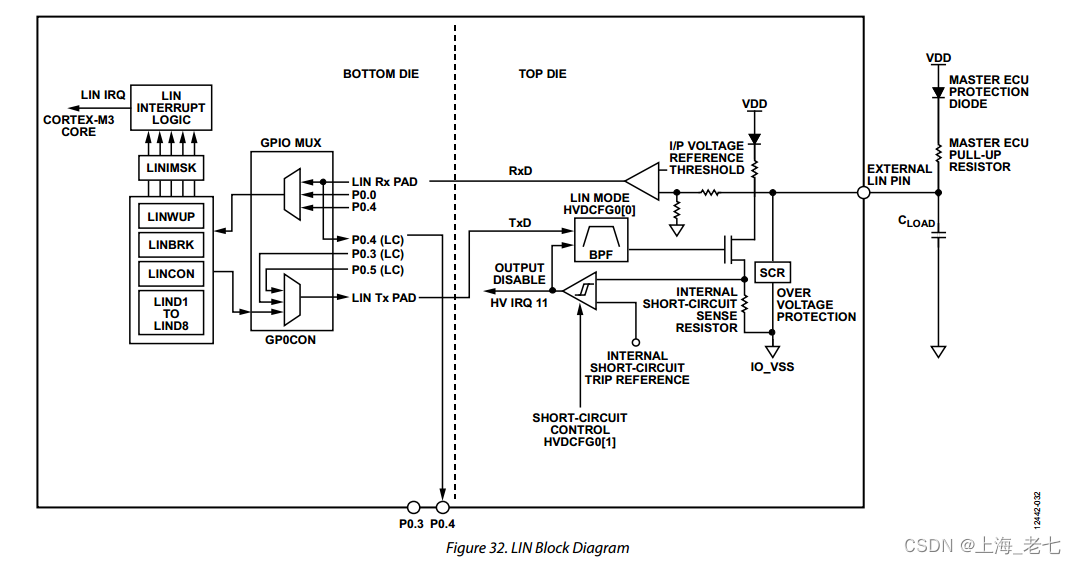
The ADuCM330/ADuCM331 implement a low overhead LIN interface that is compliant with LIN 1.3 and LIN 2.2/SAE J2602-2 specifications. The device operates as a slave only interface, operating from 1 kbps to 20 kbps. All lower rates are interpreted as 1 kbps.
The interface consists of a two die solution. As shown in Figure 32, an integrated LIN transceiver is present on the top die that Communicates directly to the LIN logic on the bottom die. The logic uses three internal Cortex-M3 interrupts, LININT0, LININT1, and LININT2, to signify to the core that a LIN event has occurred.
ADuCM330/ADuCM331采用低开销LIN接口,符合LIN 1.3和LIN 2.2/SAE J2602-2规范。该器件仅作为从机接口运行,工作频率范围为 1 kbps 至 20 kbps。所有较低的速率都被解释为 1 kbps。
该接口由双芯片解决方案组成。如图32所示,顶部芯片上有一个集成的LIN收发器,该收发器直接与底部芯片上的LIN逻辑通信。该逻辑使用三个内部 Cortex-M3 中断(LININT0、LININT1 和 LININT2)向内核表示发生了 LIN 事件。
2.2 LIN FEATURES通信特征
• Efficient LIN data handling with storage for up to eight data bytes
• Built in parity check for PID
• Framing error checking
• Running checksum (classic or enhanced) on received bytes
• Partial PID decoding to determine diagnostic master request frame
• Break symbol detection at any time
• Collision detection
• UART mode
• Automatic transceiver delay time compensation
• 高效的LIN数据处理,存储多达8个数据字节
• 内置PID奇偶校验
• 成帧错误检查
• 对收到的字节运行校验和(经典或增强)
• 部分 PID 解码以确定诊断主请求帧
• 随时检测中断符号
• 碰撞检测
• UART 模式
• 自动收发器延迟时间补偿
2.3 LIN USER OPERATION用户操作
2.3.1 LIN Transmission传输
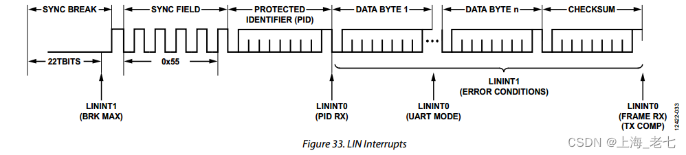
A maskable software interrupt (LININT0) occurs on the reception of a PID. After identifying the PID, the user code determines if the device must respond, receive, or ignore the PID. If a transmission is required, the user code must do the following:
• Set the number of bytes to transmit in the LINCNT register.
• Place all of the data bytes to transmit into their individual LINDx registers.
• Set LINCON[1] to 1 to signify begin transmission.
When the number of data bytes transmitted is equal to the value held in LINCNT, the checksum (which is automatically calculated) is then transmitted. After the checksum is transmitted, the frame is considered complete, and the LININT0 interrupt is set again.
接收 PID 时会发生可屏蔽的软件中断 (LININT0)。识别 PID 后,用户代码确定设备是必须响应、接收还是忽略 PID。如果需要传输,用户代码必须执行以下操作:
• 在 LINCNT 寄存器中设置要传输的字节数。
• 将所有要传输的数据字节放入其各自的 LINDx 寄存器中。
• 将 LINCON[1] 设置为 1 表示开始传输。
当传输的数据字节数等于 LINCNT 中保存的值时,然后传输校验和(自动计算)。传输校验和后,认为帧已完成,并再次设置 LININT0 中断。
2.3.2 LIN Reception接收
The LIN interface automatically changes to receive mode on reception of a break symbol.
The LININT0 interrupt indicates that a PID has been received. If the software decides that full message reception is required, the expected number of bytes is placed in the LINCNT register, and the interface begins to receive all the data bytes from the master. When all expected bytes are received, the checksum calculation is started, and if it is correct, LININT0 is triggered again.
If the software determines that the PID does not require a response, the LINCNT register must be set to 0 indicating to the hardware to ignore the rest of the frame.
LIN接口在收到中断符号时自动更改为接收模式。
LININT0 中断表示已收到 PID。如果软件决定需要接收完整的消息,则预期的字节数将放置在LINCNT寄存器中,接口开始接收来自主站的所有数据字节。收到所有预期字节后,将启动校验和计算,如果正确,则再次触发 LININT0。
如果软件确定PID不需要响应,则必须将LINCNT寄存器设置为0,指示硬件忽略帧的其余部分。
2.3.3 Sleep/Wake Functionality休眠唤醒功能
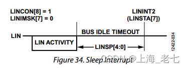
The ADuCM330/ADuCM331 LIN interface has integrated LIN sleep/wake functionality. The LININT2 interrupt is used to notify the user that a wake or sleep event has occurred. When the LININT2 interrupt is triggered, the user must interrogate the LINSTA register to determine the source of the interrupt.
The two LININT2 interrupt sources are as follows:
- The LIN interface has measured a period of inactivity on the LIN bus corresponding to the LINSLP register setting. The LINSLP register allows flexible configuring of the bus idle timeout time from 0.5 sec to 16 sec.
- The LIN interface has received a LIN wake-up frame during power-down mode. A valid wakeup is a dominant state on the LIN bus for a time set by the LINWUP register, followed by a rising edge. The LIN bus must remain high for at least two 32 kHz clock periods for the LININT2 interrupt to be generated.
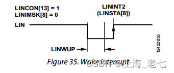
ADuCM330/ADuCM331 LIN接口集成了LIN休眠唤醒功能。LININT2 中断用于通知用户发生了唤醒或睡眠事件。触发 LININT2 中断时,用户必须询问 LINSTA 寄存器以确定中断的来源。
两个 LININT2 中断源如下所示:
1.LIN 接口在 LIN 总线上测量了与 LINSLP 寄存器设置对应的不活动时间段。LINSLP 寄存器允许灵活配置总线空闲超时时间,从 0.5 秒到 16 秒。
4. 在掉电模式下,LIN接口收到LIN唤醒帧。有效唤醒是LIN总线上由LINWUP寄存器设置的显性状态,后跟上升沿。LIN总线必须保持高电平至少两个32 kHz时钟周期,才能生成LININT2中断。
2.3.4 LIN Diagnostic Frame Support诊断帧支持
The ADuCM330/ADuCM331 LIN interface has intelligent support for diagnostic command frames (PID 0x3C) from a LIN master.
In the event a 0x3C PID is sent from the LIN master and LINCON[14] is cleared to 0, the ADuCM330/ADuCM331 cannot generate a LININT0 PID interrupt. The ADuCM330/ADuCM331 then generates a LININT0 frame received interrupt only on the following conditions:
• Byte 0: contains NAD of the IBS slave.
• Byte 0: contains 0x00 (sleep frame).
• Byte 0: contains 0x7F (broadcast frame).
All other conditions cause the entire LIN diagnostic frame to be ignored, and no interrupt is generated on the LIN frame. This feature means there is minimum software intervention in servicing LIN diagnostic frames, and ensures that the ADuCM330/ADuCM331 only
interrupts the user due to frames that are of relevance to the IBS.
This feature can be disabled by setting LINCON[14] to 1. This setting ensures that a header received interrupt occurs on all 0x3C PID headers that occur on the LIN bus.
ADuCM330/ADuCM331 LIN接口对LIN主机的诊断命令帧(PID 0x3C)提供智能支持。如果从LIN主机发送0x3C PID,并且LINCON[14]被清除为0,则ADuCM330/ADuCM331无法产生LININT0 PID 中断。然后,ADuCM330/ADuCM331仅在以下情况下生成LININT0帧接收中断条件:
• 字节 0:包含 IBS 从站的 NAD。
• 字节 0:包含0x00(休眠帧)。
• 字节 0:包含0x7F(广播帧)。
所有其他情况会导致忽略整个LIN诊断帧,并且不会在LIN帧上生成中断。此功能意味着在维护LIN诊断帧时软件干预最少,并确保ADuCM330/ADuCM331仅由于与 IBS 相关的帧而中断用户。
此功能可以通过将 LINCON[14] 设置为 1 来禁用。此设置可确保在所有LIN总线上出现的0x3C PID 帧头都会引起帧头接收中断。
2.3.5 Error Handling错误处理
The ADuCM330/ADuCM331 LIN interface is capable of handling multiple error events. The LINSTA register reflects the source of the error.The following errors can produce an interrupt:
• Collision detection: in the event of a collision during transmission, the hardware automatically ceases transmission, and a maskable LININT1 interrupt is generated.
• Maximum negative edges: if the interface receives more than the maximum negative edges expected in a LIN frame, a maskable LININT1 interrupt occurs.
• PID parity error flag: a LIN PID has two parity bits. If the received PID does not correctly match the LIN2.2 parity scheme specification, this error is flagged. A new break symbol clears this flag.
• Framing error flag: in the event of a frame error, this error is flagged. A new break symbol clears this flag.
• Checksum error: if the received checksum does not match the calculated checksum, this error condition occurs.
ADuCM330/ADuCM331 LIN接口能够处理多个错误事件。LINSTA 寄存器反映了错误的源。以下错误可能会产生中断:
• 碰撞检测:如果在传输过程中发生碰撞,硬件会自动停止传输,并且生成一个可屏蔽的 LININT1 中断。
• 最大负边沿:如果接口接收到的负边沿超过LIN帧中预期的最大负边沿,则生成一个可屏蔽的LININT1 中断。
• PID 奇偶校验错误标志:LIN PID 有两个奇偶校验位。如果收到的 PID 与 LIN2.2 奇偶校验方案不匹配规范,则标记此错误。新的中断符号将清除此标志。
• 成帧错误标志:如果发生帧错误,则会标记此错误。新的中断符号将清除此标志。
• 校验和错误:如果收到的校验和与计算的校验和不匹配,则会发生此错误情况。
2.4 LIN MEMORY MAPPED REGISTERS寄存器
LIN Memory Mapped Registers (Base Address 0x40005000)
直接对照着文档 P111到P119 看吧。
可以打印出来,写代码的时候备查。
3 HIGH VOLTAGE PERIPHERAL CONTROL INTERFACE高压外设控制接口
A high voltage peripheral is connected to the low voltage die via a serial interface. The low voltage die is the serial interface controller. The serial interface is clocked with an inter-die communication clock (DCLK) (UCLK/8)。
高压外设通过串行接口连接到低压芯片。低压芯片是串行接口控制器。该串行接口采用芯片间通信时钟 (DCLK) (UCLK/8) 进行计时。
3.1 HIGH VOLTAGE PERIPHERAL CONTROL INTERFACE OPERATION高压外设控制接口操作
The two following methods are implemented for communicating data to and from the top die of the ADuCM342:
► An indirect high voltage register access method also known as the keyhole approach, which must be used for functional safety relevant applications. The indirect access is similar to previous intelligent battery sensor devices from Analog Devices.
► A direct MMR programming method, which is not used for functional safety relevant applications.
以下两种方法,用于与ADuCM342顶部芯片传输数据:
► 一种间接高压寄存器访问方法,也称为锁孔方法,与功能安全相关的应用必须使用此方法。间接访问类似于ADI公司以前的智能电池传感器设备。
► 直接MMR编程方法,不用于功能安全相关应用。
3.1.1 Indirect Approach间接法
To read data or write data to the high voltage top die, an indirect high voltage register access method is implemented in the controller side of the interface. This means that the user must use the HVDAT register and the HVCON register on the bottom die for accessing the registers on the top die.
A high voltage register access is initiated by writing the appropriate high voltage command into the HVCON register. After writing the appropriate high voltage command into the HVCON register, the HVCON register contains information on the progress and validity of the high voltage register access. After a high voltage register is accessed, the HVDAT register contains the last executed command in Register HVDAT,Bits[11:8].
为了读取数据或将数据写入高压顶部芯片,在接口的控制器侧应用了间接高压寄存器访问方法。这意味着用户必须使用底部芯片上的HVDAT寄存器和HVCON寄存器来访问顶部芯片上的寄存器。
高压寄存器访问是通过将适当的高压命令写入 HVCON 寄存器来启动的。将适当的高压命令写入HVCON寄存器后,HVCON寄存器包含有关高压寄存器访问进度和有效性的信息。访问高压寄存器后,HVDAT 寄存器包含寄存器中最后执行的命令,Bits[11:8]。
The content of the HVDAT register after an executed high voltage command is as follows:
► High voltage read: after the high voltage register read is completed, the user can read the high voltage register data from the low byte of the HVDAT register.
► High voltage write: the data to be written to the high voltage register has to be programmed to the HVDAT register before initiating a high voltage register write.
执行高压命令后HVDAT寄存器的内容如下:
► 高压读:高压寄存器读出完成后,用户可以从HVDAT寄存器的低字节读取高压寄存器数据。
► 高压写入:在启动高压寄存器写入之前,必须将要写入高压寄存器的数据编程到HVDAT寄存器。
On a high voltage interrupt event, a high voltage read of the HVSTA register is automatically initiated. If the high voltage interface is busy, the automatic HVSTA read commences when the current command completes. After the HVSTA read completes, an interrupt is issued to the core.
Read the HVCON register to check the progress of the high voltage register access and check Register HVDAT, Bits[11:8] to confirm that the HVSTA read has been performed.
在高压中断事件中,自动启动HVSTA寄存器的高压读取。如果高压接口繁忙,则在当前命令完成时开始自动 HVSTA 读取。HVSTA 读取完成后,将向内核发出中断。
读取 HVCON 寄存器以检查高压寄存器访问的进度,并检查寄存器 HVDAT, 位 [11:8] 以确认已执行 HVSTA 读取。
3.1.2 Direct MMR Programming直接寄存器编程
This method uses the HVDCFG0 register to write data to the HVCFG0 register on the high voltage top die. Writing a value to the HVDCFG0 register automatically initiates a write to the HVCFG0 register on the high voltage die. The HVDCFG0 register on the low voltage MMR is then automatically updated to the readback value from the top die.
The HVDSTA register on the low voltage die is a shadowed register of the HVSTA register on the high voltage die. On a high voltage interrupt,an HVSTA register read is automatically initiated and the shadowed HVDSTA is updated accordingly. An HVDSTA register update only occurs with a high voltage interrupt or when an HVSTA register read via the indirect high voltage register access method is performed.
此方法使用 HVDCFG0 寄存器将数据写入高压顶部芯片上的 HVCFG0 寄存器。将值写入 HVDCFG0 寄存器会自动启动对高压芯片上的 HVCFG0 寄存器的写入。然后,低压MMR上的HVDCFG0寄存器自动更新为顶部芯片的回读值。
低压芯片上的HVDSTA寄存器是高压芯片上HVSTA寄存器的影子寄存器。在高压中断时,自动启动HVSTA寄存器读取,并相应地更新影子寄存器的HVDSTA。HVDSTA寄存器更新仅在高压中断或通过间接高压寄存器访问方法读取HVSTA寄存器时发生。
When a high voltage interrupt occurs and the automatically initiated HVSTA read is not completed, the internal hardware associated with the shadowed MMRs reiterates an HVSTA read command until an HVSTA read has been performed. In case of a fault within a high voltage peripheral control interface, this feature prevents any further high voltage communication.
Therefore, it is recommended to implement a timeout counter functionality within the high voltage communication user code, which indicates a high voltage communication fault.
A delay of 20 µs is required when using the direct high voltage register access method to ensure that data has been transferred correctly. To avoid this delay, the user can poll the HVCON register to check if the information has been written correctly.
当发生高压中断并且自动启动的 HVSTA 读取未完成时,与阴影 MMR 关联的内部硬件将重申 HVSTA 读取命令,直到 HVSTA 读取执行完毕。如果高压外设控制接口发生故障,此功能可避免任何进一步的高压通信。
因此,建议在高压通信用户代码中实现超时计数器功能,以表示高压通信故障。
使用直接高压寄存器访问方法时,需要20 μs的延迟,以确保数据已正确传输。为了避免这种延迟,用户可以轮询 HVCON 寄存器以检查信息是否已正确写入。
3.2 HIGH VOLTAGE DIE REGISTERS高压芯片寄存器
The registers residing on the high voltage die can only be accessed using the high voltage peripheral control interface.
驻留在高压芯片上的寄存器只能使用高压外设控制接口访问。
3.3 HIGH VOLTAGE PERIPHERAL CONTROL INTERFACE MEMORY MAPPED REGISTERS高压外设控制接口存储器映射寄存器
3.3.1 HVCON寄存器
Address: 0x40003004, Reset: 0x0000, Name: HVCON
If the user is using the keyhole approach, the HVCON register and HVDAT register are used together.
To write data to the HVCFG0 register on the top die, first data is placed into the HVDAT register, and then 0x08 is written into the HVCON register.
To read data from the top die registers (HVCFG0 or HVSTA), 0x00 or 0x02 is placed in the HVCON register. A data read is then triggered from the top die, and the selected register contents are copied down into the HVDAT register. Care must be taken to observe the relevant busy,P_BIT, and ACK_BIT bits of the HVCON register.
The HVCON register accepts the following commands, as shown in Table 160, when written to.
When read, the HVCON register returns a 4-bit value.
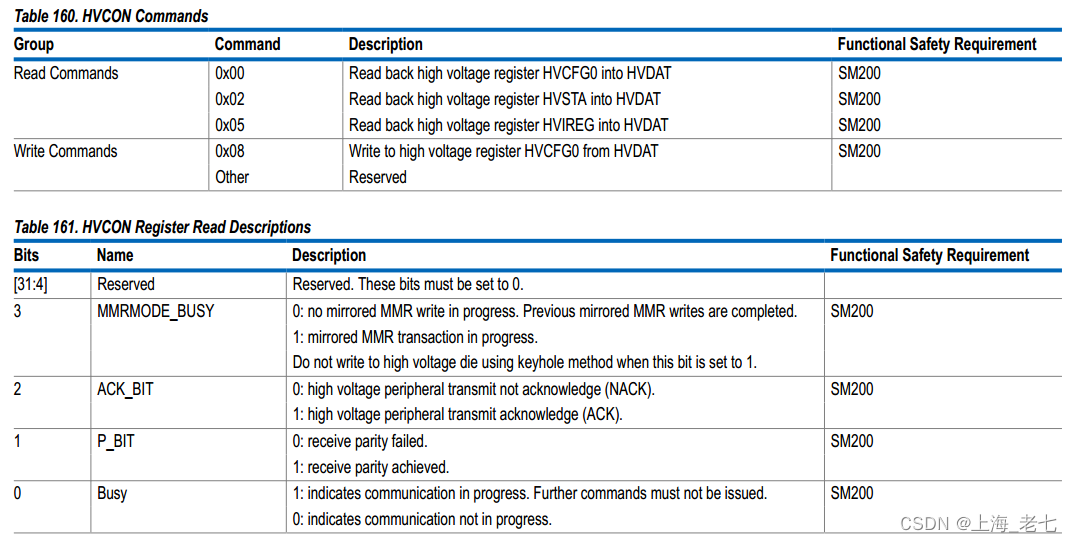
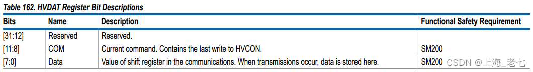
3.3.2 HVDAT寄存器
Address: 0x4000300C, Reset: 0x0800, Name: HVDAT
Register HVDAT, Bits[7:0] store the data read from or to be written to the top die.
Register HVDAT, Bits[11:8] store the last performed high voltage access command
其余各寄存器详细解释参见芯片文档。
4 EXCEPTIONS AND INTERRUPTS异常和中断
4.1 ARM CORTEX-M3 PROCESSOR AND FAULT MANAGEMENT处理器和故障管理
4.1.1 ARM Cortex-M3中断基础
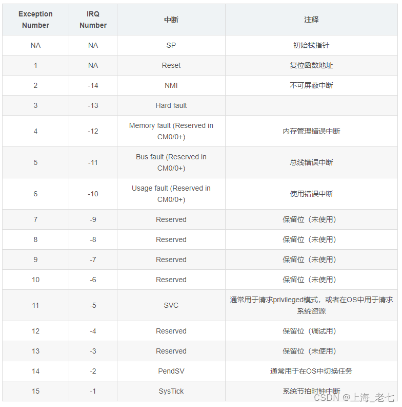
ARM Cortex-M架构的芯片的中断向量表(Interrupt Vector Table)前16位的中断由ARM核设定。16位以后的中断为芯片厂商自行定义。ARM Cortex-M架构芯片一般带有片上闪存(flash)。ARM Cortex-M手册规定在片上闪存起始地址处需要有一个有效的中断向量表。芯片上电或复位后首先从中向量表中读出入口函数地址和栈指针。将入口函数地址和栈指针装载入寻址寄存器(PC)和栈指针(SP)寄存器后,开始执行程序。
中断向量表每一位为一个32bit的地址。每一个地址对应一个中断函数的地址(第一位除外)。除了第一位以外,所有地址的目标都为寻址寄存器(PC)。当相应中断触发时,ARM Cortex-M硬件会自动把中断向量表中相应的中断函数地址装载入寻址寄存器(PC)然后开始执行中断函数。如上所述,前16位为ARM保留的系统中断,建议读者熟记。之后的中断为芯片自定义的外部中断,可以在使用时查询手册或者厂商提供的驱动程序。
中断向量表一般在芯片的startup函数中定义,可以通过汇编语言定义也可以通过C语言定义。
4.1.2 几个重要的系统异常
1.Reset
当复位后,硬件会自动把堆栈的栈顶位置放到第0个系统中断的位置并该值设置MSP,并把reset函数的地址赋给PC指针,工程代码是从Reset函数开始执行的。
*** 2.总线异常***
当总线接口传输数据时,如果回复了一个错误信号,则会产生总线异常。
可能在取指,读写数据时,及中断函数执行时的出入栈产生。
 具体工况:

a. 访问地址没有存储器。

b. 设备还没有做好传输数据的准备。

对应寄存器:BusFault Address Register,指出出问题的具体地址。
BusFault Status Register:指出具体是那种总线
3.内存使用异常:
常见于触犯了MPU设置的保护策略以及内存非法访问。
  .访问了MPU设置范围外的地址

 . 只读空间写入数据

 . 用户权限下读写特权级才能访问的地址

4. 用法异常
.执行未定义的指令
. 无效的中断返回

5. Hard fault
Hard fault会在bus,mem,usage产生且中断函数无法执行时(没有使能中断服务或者被更高优先级抢占)产生。

4.1.3 ARM CORTEX-M3 PROCESSOR AND FAULT MANAGEMENT处理器和故障管理
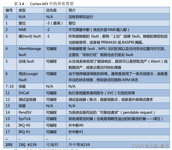
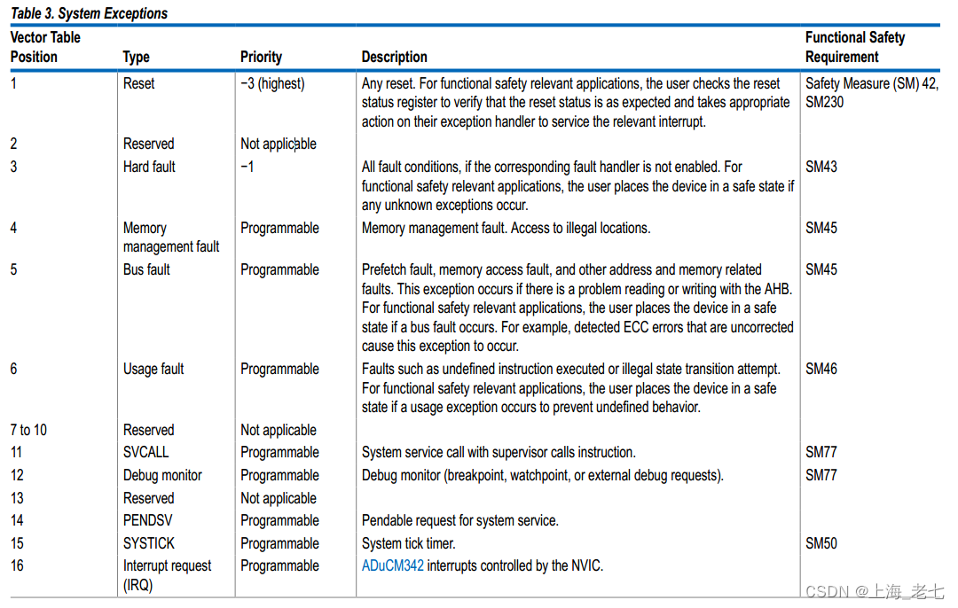
The ARM Cortex-M3 processor supports a number of system exceptions, peripherals, and external interrupts, as shown in Table 3 and Table 4.
If the appropriate handler for the fault conditions listed in Table 3 is not enabled in the system handler control and state register (SHCSR), these detected fault conditions are escalated to a hard fault.
ARM Cortex-M3 处理器支持多种系统异常、外设和外部中断,如表 3 和表 4 所示。
如果未在系统处理程序控制和状态寄存器 (SHCSR) 中启用表 3 中列出的故障条件的相应处理程序,则这些检测到的故障条件将升级为硬故障。
4.2 NESTED VECTORED INTERRUPT CONTROLLER嵌套中断向量控制器
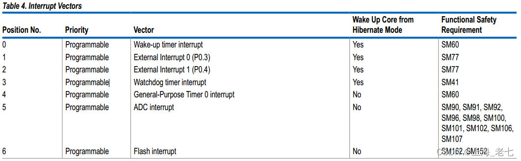
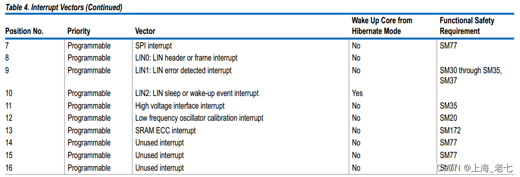
The ADuCM342 interrupts are controlled by the NVIC, and four levels of priority are available. NVIC interrupts can be enabled and disabled by writing to their corresponding interrupt set enable or interrupt clear enable register bit field. Only a limited number of interrupts can wake up the core from low power hibernate mode. These interrupts are described in Table 4. When the ADuCM342 wakes up from any mode, the device
returns to active mode
ADuCM342中断由NVIC控制,提供四个优先级级别。NVIC 中断可以通过写入中断设置使能寄存器或中断清除使能寄存器中相应位字段来使能或者禁止。只有有限数量的中断可以从低功耗休眠模式唤醒内核。表 4 描述了这些中断。当ADuCM342从任何模式唤醒时,器件返回活动模式。

For the ADuCM342, each interrupt can have eight levels of priority. The priority levels are 0 to 7, where 0 is the highest priority and 7 is the lowest priority. Internally, the highest user-programmable priority (0) is treated as fourth priority, after a reset, an NMI, and a hardware fault. Zero is the default priority for all the programmable priorities.
If the same priority level is assigned to two or more interrupts, their hardware priority (the lower the position number, the higher the priority, as shown in Table 4) determines the order in which the processor activates them. For example, if both the ADC and SPI are Priority Level 1, the ADC has higher priority.
对于ADuCM342,每个中断可以具有八个优先级级别。优先级为 0 到 7,其中 0 是最高优先级,7 是最低优先级。在内部,在复位、NMI 和硬件故障之后,最高的用户可编程优先级 (0) 被视为第四优先级。零是所有可编程优先级的默认优先级。
如果为两个或多个中断分配相同的优先级,则它们的硬件优先级(位置编号越低,优先级越高,如表 4 所示)决定了处理器激活它们的顺序。例如,如果ADC和SPI的优先级均为1级,则ADC的优先级更高。
4.3 SETTING INTERRUPT PRIORITIES中断优先级设置
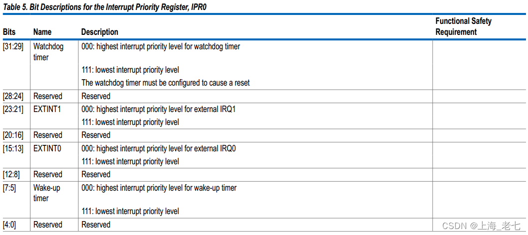
The ARM Cortex-M3 processor IPR0 register to IPR3 register control the interrupt priority settings for the ADuCM342. The user can adjust these registers to change the default interrupt priority and to create a user specific interrupt vector table to suit the application of the user.
Every interrupt has eight possible priority levels, with 0 being the highest priority and 7 being the lowest priority setting. Each interrupt priority register supports four interrupt sources. Table 5 uses IPR0 as an example to explain the relevant bits.
The IPR1 to IPR3 interrupt priority registers are configured similarly, with default priority according to Table 4.
ARM Cortex-M3处理器IPR0寄存器到IPR3寄存器控制ADuCM342的中断优先级设置。用户可以调整
这些寄存器用于更改默认中断优先级并创建用户特定的中断向量表以适应用户的应用。
每个中断都有八个可能的优先级,其中 0 表示最高优先级,7 表示最低优先级设置。每个中断优先级
寄存器支持四个中断源。表5以IPR0为例来解释相关位。
IPR1 至 IPR3 中断优先级寄存器的配置类似,默认优先级如表 4 所示。
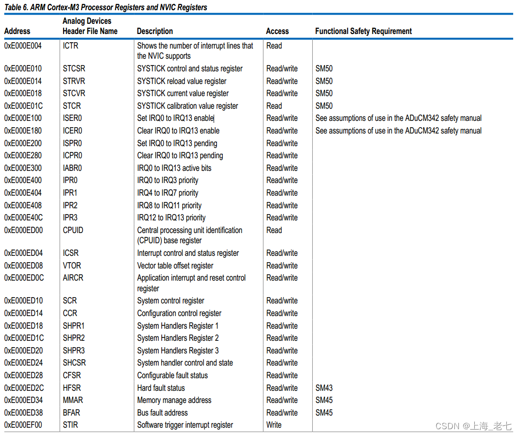
4.4 ARM CORTEX-M3 PROCESSOR AND NVIC REGISTERS中断嵌套控制寄存器
The interrupt set enable register (ISER0) and the interrupt clear enable register (ICER0) enable and disable the interrupts. The interrupt set pending register (ISPR0) and the interrupt clear pending register (ICPR0) pend the interrupts. The ISER0 register, ICER0 register, ISPR0 register, and ICPR0 register use a write 1 to enable and a write 1 to clear policy. Each bit in the interrupt set enable register corresponds to one of 32 interrupts. Setting a bit in the interrupt set enable register enables the interrupt.
中断设置使能寄存器 (ISER0) 和中断清除使能寄存器 (ICER0) 可以启用和禁用中断。中断设置挂起寄存器 (ISPR0) 和中断清除挂起寄存器 (ICPR0) 可以挂起中断。ISER0 寄存器、ICER0 寄存器、ISPR0 寄存器和 ICPR0 寄存器使用写 1 启,写 1 清除策略。中断设置使能寄存器中的每个位对应于 32 个中断中的一个。在中断设置使能寄存器(ISER0)中设置位可启用中断。
When the enable bit of a pending interrupt is set in the interrupt set pending register, the processor activates the interrupt based on the priority of the interrupt. However, if the corresponding bit is clear in the set enable register, asserting the interrupt signal pends the interrupt, but it is not possible to activate the interrupt, regardless of its priority.
当在中断设置挂起寄存器中设置某个挂起中断的使能位时,处理器根据中断的优先级激活中断。但是,如果在中断设置使能寄存器中清除了相应的位,触发中断的信号将暂停中断,但无论其优先级如何,都不可能激活中断。
Pending the interrupt means that, if the interrupt occurs, it is possible for the user code to investigate the interrupt set pending register and verify whether the interrupt occurs. Therefore, a disabled interrupt can serve as a latched general-purpose bit.
挂起中断意味着,如果发生中断,用户代码可以调查中断设置挂起寄存器并验证中断是否发生。因此,禁用的中断可以用作锁存的通用位。
Reading and clearing interrupts occur without invoking an interrupt.
读取和清除中断时无需调用中断。
Clear the enable state by writing a 1 to the corresponding bit in the interrupt clear enable register. This write also clears the corresponding bit in the interrupt set enable register. Writing to the interrupt clear pending register has no effect on an interrupt that is active, unless the interrupt is also pending. If an interrupt is active when it is disabled, the interrupt remains in its active state until cleared by a reset or an exception return.
通过在中断清除使能寄存器(ICER0)中的相应位写入 1 来清除使能状态。此写入还会清除中断设置使能寄存器中(ISER0)的相应位。写入中断清除挂起寄存器对处于活动状态的中断没有影响,除非中断也处于挂起状态。如果中断在禁用时处于活动状态,则中断将保持其活动状态,直到被重置或异常返回清除。
The NVIC is an integral part of the ARM Cortex-M3 processor. The NVIC is notified that an interrupt is generated from peripherals within one clock cycle of the clock used by this peripheral, unless otherwise noted.
NVIC是ARM Cortex-M3处理器的一个组成部分。除非另有说明,否则 NVIC 会在一个时钟周期内内收到外设生成中断的通知,该时钟周期就是外设使用的时钟周期。
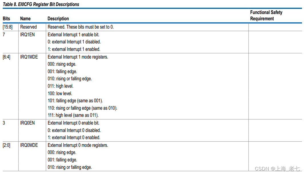
4.5 EXTERNAL INTERRUPT CONFIGURATION外部中断配置
Two external interrupts are implemented. The interrupts can be separately configured to detect any combination of the following types of events:
► Rising edge. The logic detects a transition from low to high and generates a pulse. Only one pulse is sent to the ARM Cortex-M3 processor per rising edge.
► Falling edge. The logic detects a transition from high to low and generates a pulse. Only one pulse is sent to the ARM Cortex-M3 processor per falling edge.
► Rising or falling edge. The logic detects a transition from low to high or from high to low and generates a pulse. Only one pulse is sent to the ARM Cortex-M3 processor per edge.
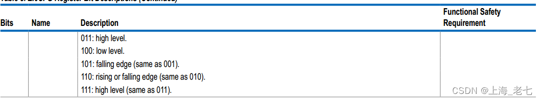
► High level. The logic detects a high level. The appropriate interrupt is asserted and sent to the ARM Cortex-M3 processor. The interrupt line is held asserted until the external source deasserts. The high level must be maintained for one core clock cycle minimum to be detected.
► Low level. The logic detects a low level. The appropriate interrupt is asserted and sent to the ARM Cortex-M3 processor. The interrupt line is held asserted until the external source deasserts. The low level must be maintained for one core clock cycle minimum to be detected.
The external interrupt detection unit block allows an external interrupt to wake up the device when in hibernate mode.
本芯片实现了两个外部中断。外部中断可以单独配置,以检测以下类型事件的任意组合:
► 上升沿。该逻辑检测从低电平到高电平的转换并产生脉冲。每个上升沿仅向 ARM Cortex-M3 处理器发送一个脉冲。
► 下降沿。该逻辑检测从高电平到低电平的转换并产生脉冲。每个下降沿仅向 ARM Cortex-M3 处理器发送一个脉冲。
►上升沿或下降沿。该逻辑检测从低到高或从高到低的转换并产生脉冲。每个上升或下降沿仅向 ARM Cortex-M3 处理器发送一个脉冲。
► 高电平。逻辑检测到高电平。相应的中断被触发并将其发送到 ARM Cortex-M3 处理器。中断线保持触发,直到外部源取消触发。必须保持高电平才能检测到一个内核时钟周期最小值。
► 低水平。逻辑检测到低电平。相应的中断被触发并将其发送到 ARM Cortex-M3 处理器。中断线保持触发,直到外部源源取消触发。必须保持低电平才能检测到一个内核时钟周期最小值。
外部中断检测单元块允许外部中断在休眠模式下唤醒设备。
注意:interrupt is asserted 应该被翻译为中断被触发。
4.6 EXTERNAL INTERRUPT CONFIGURATION MEMORY MAPPED REGISTERS外部中断配置寄存器
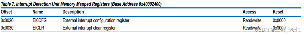
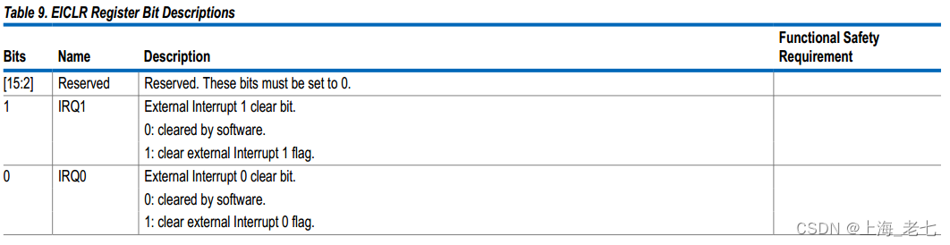
The interrupt detection unit consists of memory mapped registers (MMRs) contained in the always on section.The MMRs are based at Address 0x40002400.
由内存映射寄存器 (MMR) 组成的中断检测单元位于芯片的Always On块(常电?)中。外部中断配置寄存器的MMR 基地址是 0x40002400。
5 LIN例程
5.1 例程代码及功能描述
lin.c内容比较简单,主要实现了:
如果收到0x3D,则回复;
如果收到0x00,则存储。
//    Description  : Simple demo on how to use the LIN Interface
//					 		   : if a master sends 0x3D the M33x responds
//					 		   : if the Master sends 0x00 the m33x listens and stores the frame
/
/ Includes
#include "RTE_Components.h"             // Component selection
#include <absacc.h>

// Function Prototypes
void LIN_Init(void);

// Global Variables
unsigned char Diag_Resp[8] = {0x00,0x06,0xF2,0x3A,0x00,0x31,0x4D,0xAA};	    	// 0x3d Response
unsigned char Rx_Frame[8] = {0x00,0x00,0x00,0x00,0x00,0x00,0x00,0x00};	   		// Storage for Master Command Frame

//=====================================================================
// 						main
//=====================================================================
int main (void)
{
 T3CON = 0;  												// Turn off watchdog
 LIN_Init();												// Initialise the LIN interface

 ISER0 = 0x700;											// Enable the LIN interrupts in the NVIC
 while(1)
 {
 }
}
//=====================================================================
// 						Initialise the LIN for 20kBaud
//=====================================================================
void LIN_Init(void)
{
 unsigned int HVstatus;

 LINCON = 0x5401;													// initialise the LIN logic on bottom die

 do{
  HVDAT = 0x05;														// Enable Top Die LIN Transceiver
  HVCON = 0x08;
  do{
   HVstatus = HVCON;
  }while(HVstatus & 0x01);
 }while(!(HVstatus & 0x04));
}

//=====================================================================
// 						LINint0 event Handler, Rx and Tx sources
//=====================================================================
void LIN0_Int_Handler (void)
{
 unsigned int lcl_LINSTA;

 lcl_LINSTA = LINSTA;
 if(lcl_LINSTA & 0x1)	   									  // Header Received.
 {																					// Disable Sleep / Wake timer as LIN is running and interrupt occured.
  LINSTA |= 0x1;
  if(LINID == 0x3D)												  // 0x3D Slave Response Pending to Tx
  {
   LINCNT = 0x8;
   LIND1 = Diag_Resp[0];
   LIND2 = Diag_Resp[1];
   LIND3 = Diag_Resp[2];
   LIND4 = Diag_Resp[3];
   LIND5 = Diag_Resp[4];
   LIND6 = Diag_Resp[5];
   LIND7 = Diag_Resp[6];
   LIND8 = Diag_Resp[7];
   LINCON |= 0x03;													// Transmit
  }
 }
 if(lcl_LINSTA & 0x2)  											// Frame Received
 {
  LINSTA |= 0x2;
  if(LINID == 0x00)													// Listen to Command and store data bytes.
  {
   LINCNT = 0x8;
   Rx_Frame[0] = LIND1;
   Rx_Frame[1] = LIND2;
   Rx_Frame[2] = LIND3;
   Rx_Frame[3] = LIND4;
   Rx_Frame[4] = LIND5;
   Rx_Frame[5] = LIND6;
   Rx_Frame[6] = LIND7;
   Rx_Frame[7] = LIND8;
  }  																				// Check Diagnostic or command frame
 }
 if(lcl_LINSTA & 0x4)  											// Tx Complete
 {
  LINSTA |= 0x4;
 }
}

//=====================================================================
// 						LINint1 Error Handler
//=====================================================================
void LIN1_Int_Handler (void)
{
 LINSTA = 0xFFFF;														// Not interested in any other LINSTA status bits
}

//=====================================================================
// 						LINint2 Handler, Wake Sleep events
//=====================================================================
void LIN2_Int_Handler (void)
{
 LINSTA = 0xFFFF;													 // Not interested in any other LINSTA status bits
}

//============================================================================
//				SYSTICK Handler
//============================================================================
void SysTick_Int_Handler(void)
{
}

//=====================================================================
// 						WUP Timer Interrupt Handler
//=====================================================================
void WakeUp_Int_Handler(void)
{
}

//=====================================================================
// 						GP Timer Interrupt Handler
//=====================================================================
void GP_Tmr_Int_Handler(void)
{
}

//=====================================================================
// 						ADC Interrupt Handler
//=====================================================================
void ADC_Int_Handler(void)
{
}

//==========================================================================================
//				Hard Fault Handler, 2bit or >2bit ECC error interrupt
//==========================================================================================
void Hard_Fault_Exception(void)
{
}
5.2 头文件
5.2.1 RTE头文件的相关设置
前面包含"RTE_Components.h" ,这个文件是通过下列设置自动添加到路径、并且复制实体文件到的。
5.2.2 RTE_Components.h
主要是引用芯片头文件
#ifndef RTE_COMPONENTS_H
#define RTE_COMPONENTS_H


/*
 * Define the Device Header File:
 */
#define CMSIS_device_header "ADuCM331.h"

/* AnalogDevices::Device:Startup:1.0.0 */
#include <ADuCM331.h>


#endif /* RTE_COMPONENTS_H */
5.2.3 芯片头文件
ADuCM331.h文件位置在Keil安装目录下,导入芯片Pack包的时候复制过去的。
打开芯片头文件ADuCM331.h,可以看到LIN寄存器的名称和地址定义。
// LIN

#define          LINBASE                                    (*(volatile unsigned long      *) 0x40005000)
#define          LINBASE_A                                  0x40005000
// LIN control
#define          LINCON                                     (*(volatile unsigned short int *) 0x40005000)
#define          LINCON_A                                   0x40005000
// LIN interrupt mask
#define          LINIMSK                                    (*(volatile unsigned short int *) 0x40005004)
#define          LINIMSK_A                                  0x40005004
#if           ALLOW_DEPRECATED_NAMES
// "LINMASK" has been deprecated. Use "LINIMSK" instead.
#define          LINMASK                                    (*(volatile unsigned short int *) 0x40005004)
#define          LINMASK_A                                  0x40005004
#endif
// Baud rate count
#define          LINBR                                      (*(volatile unsigned short int *) 0x40005008)
#define          LINBR_A                                    0x40005008
// Break symbol count
#define          LINBRK                                     (*(volatile unsigned short int *) 0x4000500C)
#define          LINBRK_A                                   0x4000500C
// LIN sampling delay count
#define          LINSAMP                                    (*(volatile unsigned short int *) 0x40005014)
#define          LINSAMP_A                                  0x40005014
// Forces LIN low while its value  > 0
#define          LINFORCE                                   (*(volatile unsigned short int *) 0x40005018)
#define          LINFORCE_A                                 0x40005018
// Time of the minimum low time that will wake up the device
#define          LINWUP                                     (*(volatile unsigned short int *) 0x4000501C)
#define          LINWUP_A                                   0x4000501C
#if           ALLOW_DEPRECATED_NAMES
// "LINWKUP" has been deprecated. Use "LINWUP" instead.
#define          LINWKUP                                    (*(volatile unsigned short int *) 0x4000501C)
#define          LINWKUP_A                                  0x4000501C
#endif
// Byte count  for the entire LIN frame
#define          LINCNT                                     (*(volatile unsigned char      *) 0x40005020)
#define          LINCNT_A                                   0x40005020
// Transceiver compensation delay time
#define          LINTRDLY                                   (*(volatile unsigned char      *) 0x40005024)
#define          LINTRDLY_A                                 0x40005024
#if           ALLOW_DEPRECATED_NAMES
// "TRDLY" has been deprecated. Use "LINTRDLY" instead.
#define          TRDLY                                      (*(volatile unsigned char      *) 0x40005024)
#define          TRDLY_A                                    0x40005024
#endif
// Bus idle timeout
#define          LINSLP                                     (*(volatile unsigned char      *) 0x40005028)
#define          LINSLP_A                                   0x40005028
// Number of bytes in the last response frame
#define          LINLCNT                                    (*(volatile unsigned char      *) 0x4000502C)
#define          LINLCNT_A                                  0x4000502C
// LIN Status
#define          LINSTA                                     (*(volatile unsigned short int *) 0x40005030)
#define          LINSTA_A                                   0x40005030
// LIN Status 1
#define          LINSTA1                                    (*(volatile unsigned short int *) 0x40005038)
#define          LINSTA1_A                                  0x40005038
// PID received
#define          LINID                                      (*(volatile unsigned char      *) 0x4000503C)
#define          LINID_A                                    0x4000503C
#if           ALLOW_DEPRECATED_NAMES
// "LINPID" has been deprecated. Use "LINID" instead.
#define          LINPID                                     (*(volatile unsigned char      *) 0x4000503C)
#define          LINPID_A                                   0x4000503C
#endif
// LIN data byte 1 for Rx or Tx
#define          LIND1                                      (*(volatile unsigned char      *) 0x40005040)
#define          LIND1_A                                    0x40005040
// LIN data byte 2 for Rx or Tx
#define          LIND2                                      (*(volatile unsigned char      *) 0x40005044)
#define          LIND2_A                                    0x40005044
// LIN data byte 3 for Rx or Tx
#define          LIND3                                      (*(volatile unsigned char      *) 0x40005048)
#define          LIND3_A                                    0x40005048
// LIN data byte 4 for Rx or Tx
#define          LIND4                                      (*(volatile unsigned char      *) 0x4000504C)
#define          LIND4_A                                    0x4000504C
// LIN data byte 5 for Rx or Tx
#define          LIND5                                      (*(volatile unsigned char      *) 0x40005050)
#define          LIND5_A                                    0x40005050
// LIN data byte 6 for Rx or Tx
#define          LIND6                                      (*(volatile unsigned char      *) 0x40005054)
#define          LIND6_A                                    0x40005054
// LIN data byte 7 for Rx or Tx
#define          LIND7                                      (*(volatile unsigned char      *) 0x40005058)
#define          LIND7_A                                    0x40005058
// LIN data byte 8 for Rx or Tx
#define          LIND8                                      (*(volatile unsigned char      *) 0x4000505C)
#define          LIND8_A                                    0x4000505C
// LIN frame checksum
#define          LINFCS                                     (*(volatile unsigned char      *) 0x40005060)
#define          LINFCS_A                                   0x40005060
// Current calculated checksum
#define          LINCCS                                     (*(volatile unsigned char      *) 0x40005064)
#define          LINCCS_A                                   0x40005064
// Node ID Address
#define          LINNAD                                     (*(volatile unsigned char      *) 0x40005068)
#define          LINNAD_A                                   0x40005068
// Initial node ID
#define          LININAD                                    (*(volatile unsigned char      *) 0x4000506C)
#define          LININAD_A                                  0x4000506C
// Initial function ID
#define          LINFID                                     (*(volatile unsigned short int *) 0x40005070)
#define          LINFID_A                                   0x40005070
// Variant ID
#define          LINVID                                     (*(volatile unsigned char      *) 0x40005074)
#define          LINVID_A                                   0x40005074
// Supplier ID
#define          LINSUPID                                   (*(volatile unsigned short int *) 0x40005078)
#define          LINSUPID_A                                 0x40005078
// Service ID
#define          LINSID                                     (*(volatile unsigned char      *) 0x4000507C)
#define          LINSID_A                                   0x4000507C
5.2.4 绝对地址使用
头文件absacc.h定义了绝对地址的调用语法。
    #ifndef __at
#define __at(_addr)  __attribute__ ((at(_addr)))

#endif

#ifndef __section
#define __section(_name)  __attribute__ ((section(_name)))

#endif
也就是说,下面两句话是一样的
const unsigned int iPage0CS[2]  __at(0x07f8) = {0xffffffff,0x16400000}
const unsigned int iPage0CS[2]  __attribute__ ((at(0x07f8))) = {0xffffffff,0x16400000}
5.3 主函数
5.3.1 初始化
初始化LIN通讯,并定义通讯数组。
void LIN_Init(void);

// Global Variables
unsigned char Diag_Resp[8] = {0x00,0x06,0xF2,0x3A,0x00,0x31,0x4D,0xAA};	    	// 0x3d Response
unsigned char Rx_Frame[8] = {0x00,0x00,0x00,0x00,0x00,0x00,0x00,0x00};	   		// Storage for Master Command Frame
初始化LIN通信的子函数如下
//=====================================================================
// 						Initialise the LIN for 20kBaud
//=====================================================================
void LIN_Init(void)
{
 unsigned int HVstatus;

 LINCON = 0x5401;													// initialise the LIN logic on bottom die

 do{
  HVDAT = 0x05;														// Enable Top Die LIN Transceiver
  HVCON = 0x08;
  do{
   HVstatus = HVCON;
  }while(HVstatus & 0x01);
 }while(!(HVstatus & 0x04));
}
5.3.1.1 LINCON寄存器设置
LINCON = 0x5401 = 0B 0101 0100 0000 0001
| 位 | 15 | 14 | 13 | 12 | 11 | 10 | 9 | 8 | 7 | 6 | 5 | 4 | 3 | 2 | 1 | 0 |
|---|---|---|---|---|---|---|---|---|---|---|---|---|---|---|---|---|
| 值 | 0 | 1 | 0 | 1 | 0 | 1 | 0 | 0 | 0 | 0 | 0 | 0 | 0 | 0 | 0 | 1 |
| 含义 | TRDLY | PIDRXINT | WUPEN | TXTIMEOUT | SYNC | NAD | COLL | SLEEPEN | CSCLR | UARTEN | BYPASSEN | SYNCTIM | LEN | CSCALC | RXTXMODE | LINENABLE |
5.3.1.2 HVDAT和HVCON寄存器设置
这两个寄存器在HIGH VOLTAGE PERIPHERAL CONTROL INTERFACE章节。
对HVCON赋值时,HVCON=0x08表示将HVDAT寄存器的内容写入HVCFG0。
读HVCON的值时,bit0到bit3有不同的含义。
 do{
  HVDAT = 0x05;														// Enable Top Die LIN Transceiver
  HVCON = 0x08;
  do{
   HVstatus = HVCON;
  }while(HVstatus & 0x01);                          //当HVCON的bit0为0,即busy位为0则不执行循环;当busy为1则一直执行循环。
 }while(!(HVstatus & 0x04));                        //除非HVCON的bit2为1,即ACT_BIT为1,否则一直执行循环。
}
5.3.2 中断设置
int main (void)
{
 T3CON = 0;  												// Turn off watchdog
 LIN_Init();												// Initialise the LIN interface

 ISER0 = 0x700;											// Enable the LIN interrupts in the NVIC
 while(1)
 {
 }
}
主函数里面除了LIN初始化,还要其实就是打开LIN中断,然后在中断服务程序里面实现具体功能。
打开LIN中断通过设置ISER0寄存器进行。
ISER0 = 0x700; // Enable the LIN interrupts in the NVIC

前面讲过,NVIC 中断可以通过写入中断设置使能寄存器或中断清除使能寄存器中相应位字段来使能或者禁止。0x700 = 0b 0000 0111 0000 0000。因此,结合下表可以看出,是打开了LIN0、LIN1、LIN2三个中断。
前面讲过,ADUCM331芯片的LIN收发器直接与底部芯片上的LIN逻辑通信。该逻辑使用三个内部 Cortex-M3 中断(LININT0、LININT1 和 LININT2)向内核表示发生了 LIN 事件。
5.3.3 startup文件
上述三个LIN中断发生之后,相应的中断服务程序的名称和入口地址,在startup文件(startup_ADuCM331.s)中可以看到。
;******************************************************************************
;
; The vector table.
;
;******************************************************************************
		EXTERN SysTick_Int_Handler
		EXTERN GP_Tmr_Int_Handler
		EXTERN ADC_Int_Handler
		EXTERN WakeUp_Int_Handler
		EXTERN LIN0_Int_Handler
		EXTERN LIN1_Int_Handler
		EXTERN LIN2_Int_Handler
		EXTERN Hard_Fault_Exception

        EXPORT  __Vectors
__Vectors
        DCD     StackMem + Stack            ; Top of Stack
        DCD     Reset_Handler               ; Reset Handler
        DCD     NmiSR                       ; NMI Handler
        DCD     Hard_Fault_Exception        ; Hard Fault Handler
        DCD     MEMDefaultHandler           ; MPU Fault Handler
        DCD     BUSDefaultHandler           ; Bus Fault Handler
        DCD     USGDefaultHandler           ; Usage Fault Handler
        DCD     0                           ; Reserved
        DCD     0                           ; Reserved
        DCD     0                           ; Reserved
        DCD     0                           ; Reserved
        DCD     IntDefaultHandler           ; SVCall Handler
        DCD     IntDefaultHandler           ; Debug Monitor Handler
        DCD     0                           ; Reserved
        DCD     IntDefaultHandler           ; PendSV Handler
        DCD     SysTick_Int_Handler         ; SysTick Handler

        DCD     WakeUp_Int_Handler          ; Wake Up Timer 		[ 0]
        DCD     IntDefaultHandler           ; External Interrupt 0	[ 1]
        DCD     IntDefaultHandler           ; External Interrupt 1	[ 2]
        DCD     IntDefaultHandler           ; Watch Dog Timer		[ 3]
        DCD     GP_Tmr_Int_Handler          ; General Purpose Timer	[ 4]
        DCD     ADC_Int_Handler             ; ADC					[ 5]
        DCD     IntDefaultHandler           ; FLASH Controller		[ 6]
        DCD     IntDefaultHandler           ; SPI					[ 7]
        DCD     LIN0_Int_Handler            ; LIN 0					[ 8]
        DCD     LIN1_Int_Handler            ; LIN 1					[ 9]
        DCD     LIN2_Int_Handler            ; LIN 2					[10]
        DCD     IntDefaultHandler           ; 2WI					[11]
        DCD     IntDefaultHandler           ; CALOSC				[12]
        DCD     IntDefaultHandler           ; SRAM ECC				[13]
这是一段汇编语言,主要用到DCD指令。
简介:
DCD:数据定义( Data Definition )伪指令
一般用于为特定的数据分配存储单元,同时可完成已分配存储单元的初始化。
语法格式:
标号 DCD(或 DCDU) 表达式
DCD(或 DCDU)伪指令用于分配一片连续的字存储单元(32bit)并用指定的表达式初始化。其中表达式可以为程序标号或数字表达式。 DCD 也可用 “ &” 代替。
用 DCD 分配的字存储单元是字对齐的,而用 DCDU 分配的字存储单元并不严格字对齐。
DCD指令类似于C中定义数组并初始化。比如: DCD 0 的意思是:分配一个字存储单元,并将该单元初始化为0。
这段代码的作用就是分配ADUCM331的中断向量表地址。从DCD后面表达式的名称可以看出第一个字存储单元分配给了栈顶,第二个字分配给了复位地址,后面接着分配给其他异常或中断。和前面介绍讲的ARM Cortex-M3 处理器的系统异常,以及ADUCM342的外部中断(IRQ0到IRQ13 )一一对应。
这里的Reset_Handler,NmiSR等,其实是一个地址值,也就是中断处理函数的入口地址。在函数实现时,由编译器分配一个地址值。
从startup中断向量表的定义中可以看出,以下几个中断服务程序需要给出定义。
		EXTERN SysTick_Int_Handler
		EXTERN GP_Tmr_Int_Handler
		EXTERN ADC_Int_Handler
		EXTERN WakeUp_Int_Handler
		EXTERN LIN0_Int_Handler
		EXTERN LIN1_Int_Handler
		EXTERN LIN2_Int_Handler
		EXTERN Hard_Fault_Exception
5.3.4 中断服务程序
在主文件lin.c中,主要是处理LIN0、LIN1、LIN2三个中断,其他几个中断服务程序都是空的。

接收 PID 时会发生可屏蔽的软件中断 (LININT0)。识别 PID 后,用户代码确定设备是必须响应、接收还是忽略 PID。如果需要传输,用户代码必须执行以下操作:
• 在 LINCNT 寄存器中设置要传输的字节数。
• 将所有要传输的数据字节放入其各自的 LINDx 寄存器中。
• 将 LINCON[1] 设置为 1 表示开始传输。
当传输的数据字节数等于 LINCNT 中保存的值时,然后传输校验和(自动计算)。传输校验和后,认为帧已完成,并再次设置 LININT0 中断。
LIN接口在收到中断符号时自动更改为接收模式。
LININT0 中断表示已收到 PID。如果软件决定需要接收完整的消息,则预期的字节数将放置在LINCNT寄存器中,接口开始接收来自主站的所有数据字节。收到所有预期字节后,将启动校验和计算,如果正确,则再次触发 LININT0。
如果软件确定PID不需要响应,则必须将LINCNT寄存器设置为0,指示硬件忽略帧的其余部分。
//=====================================================================
// LINint0 event Handler, Rx and Tx sources
//=====================================================================
void LIN0_Int_Handler (void)
{
unsigned int lcl_LINSTA;
lcl_LINSTA = LINSTA;
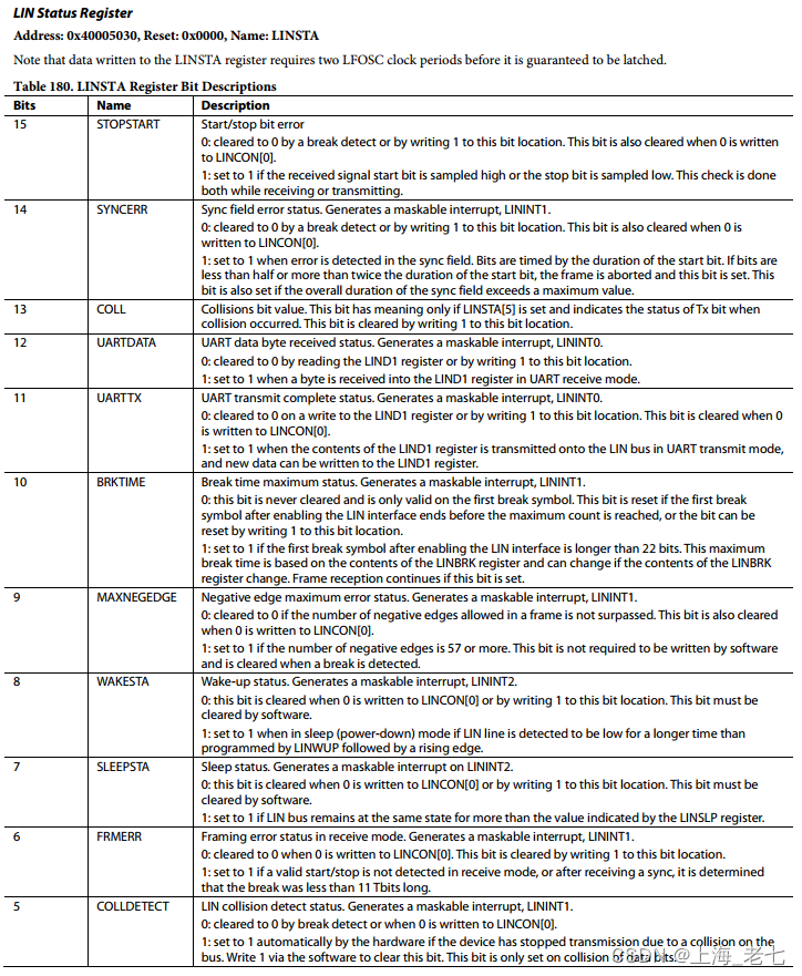
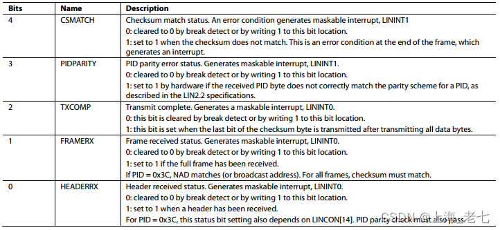
//参见LINSTA寄存器位说明,LINSTA的bit0表示帧头接收完成
if(lcl_LINSTA & 0x1) // Header Received.
{ // Disable Sleep / Wake timer as LIN is running and interrupt occured.
//参见LINSTA寄存器位说明,LINSTA的bit0写入1,会把LINSTA的bit0清为0,这样后续再收到帧头会再次触发中断。
LINSTA |= 0x1;
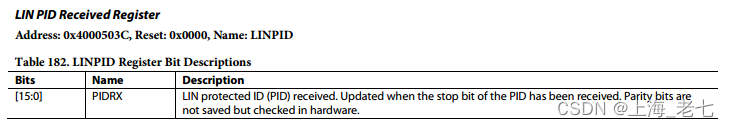
//在本例程代码中,LIN PID received register的名称为LINID,lin.c和头文件ADUCM331.h中都是这个。
//在说明文档中前后不一致,总表中是LINID,详细说明处写的是LINPID
//在后续芯片ADUCM342中,该寄存器名称统一使用LINPID。
if(LINID == 0x3D) // 0x3D Slave Response Pending to Tx
{
//如果需要传输,用户代码必须执行以下操作:
// 在 LINCNT 寄存器中设置要传输的字节数。
// 将所有要传输的数据字节放入其各自的 LINDx 寄存器中。
// 将 LINCON[1] 设置为 1 表示开始传输。
LINCNT = 0x8;
LIND1 = Diag_Resp[0];
LIND2 = Diag_Resp[1];
LIND3 = Diag_Resp[2];
LIND4 = Diag_Resp[3];
LIND5 = Diag_Resp[4];
LIND6 = Diag_Resp[5];
LIND7 = Diag_Resp[6];
LIND8 = Diag_Resp[7];
LINCON |= 0x03; // Transmit
}
}
//参见LINSTA寄存器位说明,LINSTA的bit1表示应答接收完成
if(lcl_LINSTA & 0x2) // Frame Received
{
//参见LINSTA寄存器位说明,LINSTA的bit1写入1,会把LINSTA的bit1清为0,这样后续再收到应答会再次触发中断。
LINSTA |= 0x2;
if(LINID == 0x00) // Listen to Command and store data bytes.
{
//如果软件决定需要接收完整的消息,则预期的字节数将放置在LINCNT寄存器中,接口开始接收来自主站的所有数据字节。
LINCNT = 0x8;
Rx_Frame[0] = LIND1;
Rx_Frame[1] = LIND2;
Rx_Frame[2] = LIND3;
Rx_Frame[3] = LIND4;
Rx_Frame[4] = LIND5;
Rx_Frame[5] = LIND6;
Rx_Frame[6] = LIND7;
Rx_Frame[7] = LIND8;
} // Check Diagnostic or command frame
}
//参见LINSTA寄存器位说明,LINSTA的bit2表示发送完成
if(lcl_LINSTA & 0x4) // Tx Complete
{
//参见LINSTA寄存器位说明,LINSTA的bit2写入1,会把LINSTA的bit2清为0。
LINSTA |= 0x4;
}
}
//=====================================================================
// LINint1 Error Handler
//=====================================================================
void LIN1_Int_Handler (void)
{
LINSTA = 0xFFFF; // Not interested in any other LINSTA status bits
}
//=====================================================================
// LINint2 Handler, Wake Sleep events
//=====================================================================
void LIN2_Int_Handler (void)
{
LINSTA = 0xFFFF; // Not interested in any other LINSTA status bits
}


 1013
1013


 被折叠的 条评论
为什么被折叠?
被折叠的 条评论
为什么被折叠?
 到【灌水乐园】发言


