海力士内存颗粒 编码含义解释(DDR4)

本文详细解析了海力士DDR4内存颗粒的14位编码规则,包括容量、封装、批次、速度和温度/能耗指标,以帮助用户理解和辨识不同规格的颗粒。

摘要生成于 C知道 ,由 DeepSeek-R1 满血版支持, 前往体验 >

一、含义解释

“海力士DDR4颗粒编码一共14位。前4位基本是固定的,不用看,我们看后10位——AG8NMJRVKC(第5-第14位)。第5、6、7位表示颗粒容量参数,这里AG8表示颗粒16GbX8。第8位,表示Die的封装方式,这里N表示非TSV高密度封装。第9位,表示DIE的批次,这里是M,表示1st,第一等级/批次。第10位,表示封装类型,这里J,表示倒装。第11位,表示封装材料,这里R表示,无铅无卤符合ROHS标准。第12、13位,表示速度,这里VK表示DDR4-2666 19-19-19。第14位,表示工作温度和能源消耗,这里C,表示适合工作环境0-85摄氏度(消费级颗粒),能源消耗正常。”

二、官网截图

图片截取自海力士官网
图片截取自海力士官网
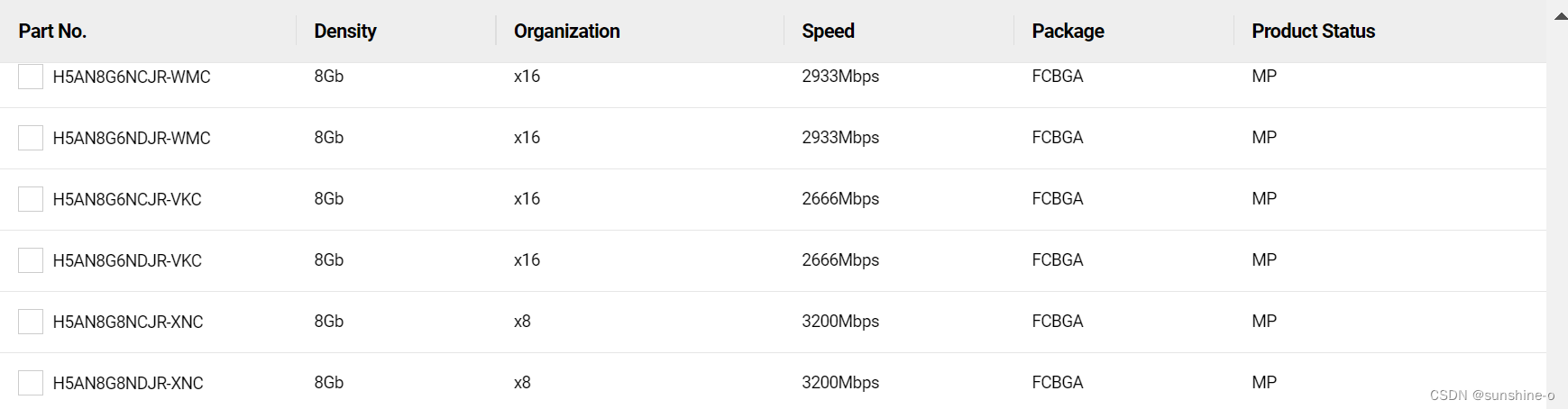
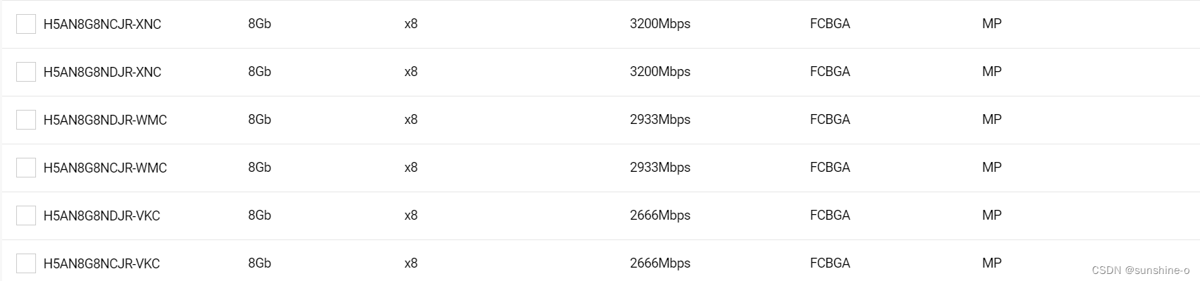
路径:海力士–PRODUCTS–DRAM–DDR–DDR4

The DDR4 SDRAM is a high-speed dynamic random-access memory internally configured as sixteen-banks, 4 bank group with 4 banks for each bank group for x4/x8 and eight-banks, 2 bank group with 4 banks for each bankgroup for x16 DRAM. The DDR4 SDRAM uses a 8n prefetch architecture to achieve high-speed operation. The 8n prefetch architecture is combined with an interface designed to transfer two data words per clock cycle at the I/O pins. A single read or write operation for the DDR4 SDRAM consists of a single 8n-bit wide, four clock data transfer at the internal DRAM core and eight corresponding n-bit wide, one-half clock cycle data transfers at the I/O pins. Read and write operation to the DDR4 SDRAM are burst oriented, start at a selected location, and continue for a burst length of eight or a ‘chopped’ burst of four in a programmed sequence. Operation begins with the registration of an ACTIVATE Command, which is then followed by a Read or Write command. The address bits registered coincident with the ACTIVATE Command are used to select the bank and row to be activated (BG0-BG1 in x4/8 and BG0 in x16 select the bankgroup; BA0-BA1 select the bank; A0-A17 select the row; refer to “DDR4 SDRAM Addressing” on datasheet). The address bits registered coincident with the Read or Write command are used to select the starting column location for the burst operation, determine if the auto precharge command is to be issued (via A10), and select BC4 or BL8 mode ‘on the fly’ (via A12) if enabled in the mode register. Prior to normal operation, the DDR4 SDRAM must be powered up and initialized in a predefined manner. The following sections provide detailed information covering device reset and initialization, register definition, command descriptions, and device operation.
评论
添加红包

请填写红包祝福语或标题

红包个数最小为10个

红包金额最低5元

当前余额3.43前往充值 >
需支付:10.00
成就一亿技术人!
领取后你会自动成为博主和红包主的粉丝 规则
hope_wisdom
发出的红包
实付
使用余额支付
点击重新获取
扫码支付
钱包余额 0

抵扣说明:

1.余额是钱包充值的虚拟货币,按照1:1的比例进行支付金额的抵扣。
2.余额无法直接购买下载,可以购买VIP、付费专栏及课程。

余额充值