


一:介绍
FMC(FPGA Mezzanine Card)标准规定了机械和电气规范。机械上有尺寸及接口布局标准,确保兼容性。电气特性涵盖高速信号传输(支持多种协议,速率高)和电源分配要求。应用于通信、工业控制、测试测量等领域,可实现功能扩展与高速连接,提升系统性能。
二:管脚分配
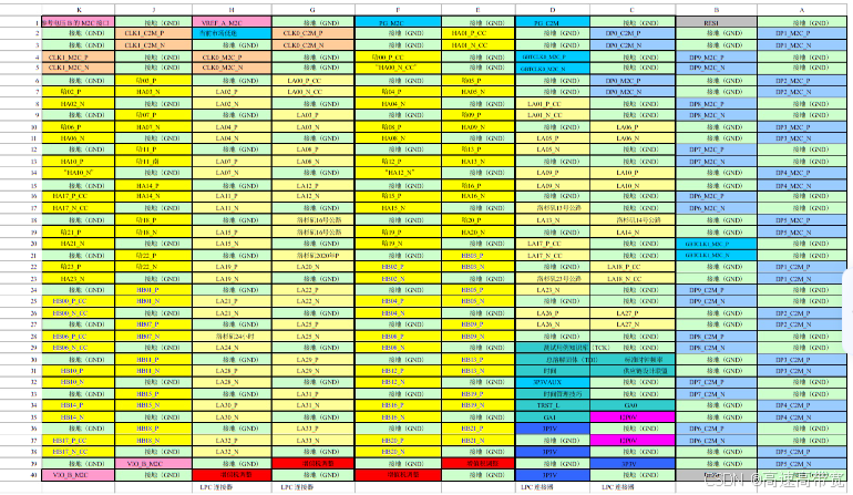
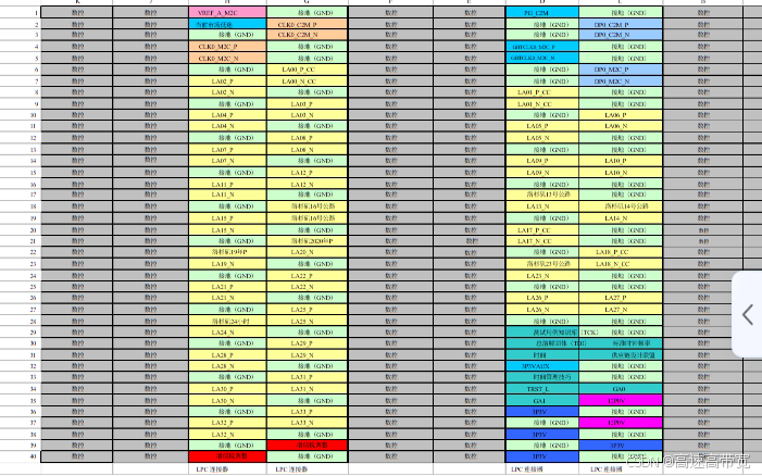
三:管脚定义
HA[00..23]_P, HA[00..23]_N - 位于高性能计算(HPC)上的 bank A 的用户自定义信号。
HB[00..21]_P, HB[00..21]_N - 位于高性能计算(HPC)上的bank B 的用户自定义信号。
CLK0_C2M_P, CLK0_C2M_N
– A differential pair that is assigned for a clock signal, which is driven from the carrier card to the IO Mezzanine Module.
CLK0_M2C_P, CLK0_M2C_N
– A differential pair that is assigned for a clock signal, which is driven from the IO Mezzanine Module to the carrier card
DP[0..9]_M2C_P, DP[0..9]_M2C_N, DP[0..9]_C2M_P, DP[0..9]_C2M_N
- These signals form 10 multi-gigabit transceiver data pairs.
GA[0..1] - These signals provide geographical addressed of the module and are used for I2C channel select.
VREF_A_M2C – This is the reference voltage associated with the signaling standard used by the bank A data pins, LAxx and HAxx. If the signaling standard on Bank A does not require a reference voltage then this pin can be left unconnected
VIO_B_M2C – This voltage is generated by the Mezzanine module and is used as the main voltage to power the IO banks on the FPGA that interface to the Bank B IO pins of the connector
VADJ
– These pins carry an adjustable voltage level power from the carrier to the IO Mezzanine module.
3P3V
– These pins carry 3.3V power from the carrier to the IO Mezzanine module
12P0V
– These pins carry 12V power from the carrier to the IO Mezzanine module.
TRST_L
- JTAG Reset. This signal provides asynchronous initialization of the TAP controller on the IO Mezzanine module.
TCK
- JTAG Clock. This signal provides an independent clock reference for TAP controller operation.
TMS
- JTAG Mode Select. This signal shall provide state control of the TAP controller on the IO Mezzanine module.
TDI
- JTAG Data In. This signal provides for serial writes of test data and instructions into the IO Mezzanine module.
TDO
- JTAG Data Out. This signal provides for serial writes of test data and instructions out of the IO Mezzanine module.
PRSNT_M2C_L
- Module present signal. This signal allows the carrier to determine whether an IO Mezzanine module is present.
PG_C2M
– Power Good Carrier Card. This signal asserts high by the carrier card when power supplies, VADJ, 12P0V, 3P3V, are within tolerance.
PG_M2C
– Power Good Mezzanine. This signal asserts high by the mezzanine module when power supplies, VIO_B_M2C, VREF_A_M2C,VREF_B_M2C, are within tolerance.
SCL
– System Management I2C serial clock. This signal provides a clock reference to the IO Mezzanine module from the carrier card for a two-wire serial management bus.
SDA
- System Management I2C serial data. This signal provides a data line for a twowire serial management bus.
RES0, RES1
– These are reserved pins and are left unconnected by the IO Mezzanine module and the carrier card.
GND
– This is signal ground
四:管脚规则
Rule 5.1:
Signal assignment for high-pin count connector shall be defined
as shown in Table 2.
Rule 5.2:
Signal assignment for low-pin count connector shall be defined as
shown in Table 3.
Observation 5.1:
Rows A through to Row K are associated with the high
pin count connectors.
Observation 5.2:
Rows C, D, G, and H are the only rows associated with
the low-pin count connectors.
Observation 5.3:
Signal names with ‘C2M’ indicate that the signal is
driven by the carrier card and received by the IO mezzanine module
Observation 5.4:
Signal names with ‘M2C’ indicate that the signal is
driven by the IO mezzanine module and received by the carrier card
Observation 5.5:
The postfix ‘_P’ on a differential signal pairs, indicates
the positive component of a differential signal
Observation 5.6:
The postfix ‘_N’ on a differential signal pairs, indicates
the negative component of a differential signal
Observation 5.7:
The postfix ‘_L’ on a single ended signal,
‘PRSNT_M2C_L’ and ‘TRST_L’ indicate that these are active low signals.
Recommendation
5.1:
Signals with a ‘_CC’ postfix should be used as the
preferred signals for clocks in source synchronous applications and should
be connected to pins on the FPGA, which are identified for this purpose
五:用户自定义管脚
LA[00..33]_P, LA[00..33]_N
- These signals are arranged as differential pairs with signals having the ‘_P’ postfix representing the positive component and signals with ‘_N’ postfix representing the negative component.
HA[00..23]_P, HA[00..23]_N
- These signals are arranged as differential pairs with signals having the ‘_P’ postfix representing the positive component and signals with ‘_N’ postfix representing the negative component.
HB[00..21]_P, HB[00..21]_N
- These signals are arranged as differential pairs with signals having the ‘_P’ postfix representing the positive component and signals with ‘_N’ postfix representing the negative component.
六:用户自定义管脚规则
Rule 5.3:
Pins with a LA or HA prefix shall use the signaling standard
associated with ‘Bank A’ and can use the reference voltage on pin
‘VREF_A_M2C’.
Rule 5.4:
Pins with a HB prefix shall use the signaling standard associated
with ‘Bank B’ and can use the reference voltage on pin ‘VREF_B_M2C’.
Rule 5.5:
Pins with a L prefix shall have connector contacts populated in
the low-pin and high-pin count connectors.
Rule 5.6:
Pins with a H prefix shall have connector contacts populated only
in the high-pin count connector.
Rule 5.7:
The high-pin count connector shall support 160 single-ended user
defined signals; or 80 differential user defined signals.
Rule 5.8:
The low-pin count connector shall support 68 single-ended user
defined signals; or 34 differential user defined signals.
Rule 5.9:
The FMC User Defined signals in Bank A shall tolerate signal
levels from -300mV to VADJ + 300mV.
Rule 5.10:
Neither the carrier nor the mezzanine module shall generate
signals outside the range of -300mV to VADJ + 300mV signal levels on the
user defined signals in Bank A.
Rule 5.11:
The FMC User Defined signals in Bank B shall tolerate signal
levels from -300mV to VIO_B_M2C + 300mV.
Rule 5.12:
Neither the carrier nor the mezzanine module shall generate
signals outside the range of -300mV to VIO_B_M2C + 300mV signal levels
on the user defined signals in Bank B.
Rule 5.13:
A minimum of no user defined signals shall be supported by this
standard.
Rule 5.14:
A maximum of 160 user defined signals shall be supported this
standard.
Permission 5.1:
Any number of user defined pins may be connected on the
FMC module or FMC carrier card.
Rule 5.15:
The user defined signals on Bank A shall be assigned starting
with the lowest ordinal in the LA group and used in ascending order. This
will be followed by signals with the lowest ordinal in the HA group and
used in ascending order.
Rule 5.16:
The user defined signals on Bank B shall be assigned starting
with the lowest ordinal in the HB group and used in ascending order.
Rule 5.17:
If an odd number of signals are assigned in Bank A or Bank B
then the ‘_P’ signal shall be populated in preference to the ‘_N’ signal.
Permission 5.2:
Bank A and Bank B may be populated independently.
Permission 5.2:
To maximize signal integrity, the LA signals should be
fully populated and then HA and HB should be populated in the same ratio
of their maximum.
Recommendation 5.3:
When signals are routed differentially each pair
should provide a differential impedance of 100Ω +/- 10%
Recommendation 5.4:
When signals are routed single ended each signal
should provide an impedance of 50Ω +/- 10%
Observation 5.8:
To maximize compatibility between mezzanine modules
and carrier cards, the LVDS and LVTTL signaling standards should be the
preferred choice.
Observation 5.9:
To maximize the performance of data buses located on
the user defined pins, the skew between user defined pins should be keep to
a minimum. The skew should be less that 10% of the targeted unit interval,
UI for the data rates on the pins. Table 4 provides examples of times for
targeted data rates.


 2399
2399

 被折叠的 条评论
为什么被折叠?
被折叠的 条评论
为什么被折叠?
 到【灌水乐园】发言


