


笔记
1、学习FPGA必须把单片机的想法完全放下,单片机是完全的顺序执行,而FPGA则是完全的并行,这是必须要深刻意识到了第一的问题;
2、语言结构(低级建模为例):低级建模又称为“ 自底向上” 的设计方法。
低级建模的基本单元有:功能模块,控制模块,组合模块。功能模块的内容包含了最基本的动作;控制模块的内容包含了动作的控制步骤;组合模块的内容包含了所有功能模块和控制模块之间的组合。
建模层次有:基础(模块)建模,仿顺序操作建模,接口建模,系统建模。基础(模块)建模的内容包含了最小功能的模块;仿顺序操作建模,这一个比较特别,主要是模仿了C语言中的函数;接口建模的内容包含了一个已经封装完成的模块;系统建模的内容包含了一个特定功能的模块
3、建模模板:仿利用VerilogHDL语言自身的特质去模仿一些顺序语言如C语言, 故称为“ 仿顺序操作”。
always@(posedge CLK or negedge RSTn)
    if(!RSTn)
        begin
            i<=4'd0;
            ....
        end
    else
        case(i)
            0:
            begin....i<=i+1'b1;end
            1:
            .....
永远的流水灯
最近入手了一块FPGA的学习板,开发板大同小异,FPGA的原理是不变的。
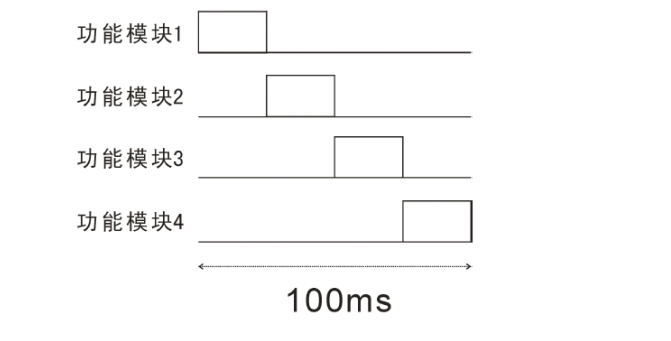
功能1:实现0.1s的四灯流水效果
并行工作示意图
代码如下:
led0_module
//led0_module
        //第一个灯亮0-0.025毫秒

        module led0_module
        (
            CLK,RSTn,LED_Out
        );
            input CLK;
            input RSTn;
            output LED_Out;
        /*************************************************/
        //db4ce15 开发板使用 晶振为50Mhz(50_000_000)  50Mhz*0.1  = 5_000_000
            parameter T100MS = 23'd5_000_000;
            /*****************100MS定时*****************/
        reg[22:0]Count1;//定义22位的寄存器 0~2^22-1

        always@(posedge CLK or negedge RSTn)   //在CLK   posedge上升沿触发 或 RSTn  negedge 下降沿触发
        if(!RSTn)
                Count1 <= 23'd0;
            else if(Count1 == T100MS)
                Count1 <=23'd0;
            else
                Count1 <= Count1+1'd1;

    /*******************************************/
    /************第一个灯亮0-0.025毫秒***********/
        reg rLED_Out;

        always@(posedge CLK or negedge RSTn)   //在CLK   posedge上升沿触发 或 RSTn  negedge 下降沿触发
        if(!RSTn)
                rLED_Out <=1'b0;
            else if(Count1>=23'd0&&Count1<=23'd1_250_000)       //第一个灯亮0-0.025毫秒
                rLED_Out <=1'b1;
            else
                rLED_Out <=1'b0;
    /*********************************************/


        assign LED_Out   = rLED_Out;
    /******************************************/
    endmodule
led1_module
    //实现目的:0.1s一个循环,4个灯,
    //第二个灯亮0.025-0.05毫秒
    module led1_module
    (
        CLK,RSTn,LED_Out
    );
        input CLK;
        input RSTn;
        output LED_Out;
    /*************************************************/
    //db4ce15 开发板使用 晶振为50Mhz 50Mhz*0.1  = 5_000_000 (50_000_000) ???
        parameter T100MS = 23'd5_000_000;
    /*****************100MS定时*****************/


        reg[22:0]Count1;//定义22位的寄存器 0~2^22-1

        always@(posedge CLK or negedge RSTn)   //在CLK   posedge上升沿触发 或 RSTn  negedge 下降沿触发
        if(!RSTn)
                Count1 <= 23'd0;
            else if(Count1 == T100MS)
                Count1 <=23'd0;
            else
                Count1 <= Count1+1'd1;

    /*******************************************/
    /************第二个灯亮0.025-0.05毫秒***********/
        reg rLED_Out;

        always@(posedge CLK or negedge RSTn)   //在CLK   posedge上升沿触发 或 RSTn  negedge 下降沿触发
        if(!RSTn)
                rLED_Out <=1'b0;
            else if(Count1>=23'd1_250_000&&Count1<=23'd2_500_000)       //第二个灯亮0.025-0.05毫秒
                rLED_Out <=1'b1;
            else
                rLED_Out <=1'b0;
    /*********************************************/


        assign LED_Out   = rLED_Out;
    /******************************************/
    endmodule
led2_module
//实现目的:0.1s一个循环,4个灯,
    //第三个灯亮0.05-0.075毫秒
    module led2_module
    (
        CLK,RSTn,LED_Out
    );
        input CLK;
        input RSTn;
        output LED_Out;
    /*************************************************/
    //db4ce15 开发板使用 晶振为50Mhz 50Mhz*0.1  = 5_000_000 (50_000_000) ???
        parameter T100MS = 23'd5_000_000;
    /*****************100MS定时*****************/

        reg[22:0]Count1;//定义22位的寄存器 0~2^22-1

        always@(posedge CLK or negedge RSTn)   //在CLK   posedge上升沿触发 或 RSTn  negedge 下降沿触发
        if(!RSTn)
                Count1 <= 23'd0;
            else if(Count1 ==T100MS)
                Count1 <=23'd0;
            else
                Count1 <= Count1+1'd1;

    /*******************************************/
    /************第三个灯亮0.05-0.075毫秒***********/
        reg rLED_Out;

        always@(posedge CLK or negedge RSTn)   //在CLK   posedge上升沿触发 或 RSTn  negedge 下降沿触发
        if(!RSTn)
                rLED_Out <=1'b0;
            else if(Count1>=23'd2_500_000&&Count1<=23'd3_750_000)       //第三个灯亮0.05-0.075毫秒
                rLED_Out <=1'b1;
            else
                rLED_Out <=1'b0;
    /*********************************************/


        assign LED_Out   = rLED_Out;
    /******************************************/
    endmodule
led3_module
//实现目的:0.1s一个循环,4个灯,
    //第四个灯亮0.075-0.1毫秒
    module led3_module
    (
        CLK,RSTn,LED_Out
    );
        input CLK;
        input RSTn;
        output LED_Out;
    /*************************************************/
    //db4ce15 开发板使用 晶振为50Mhz 50Mhz*0.1  = 5_000_000 (50_000_000) ???
        parameter T100MS = 23'd5_000_000;
    /*****************100MS定时*****************/


        reg[22:0]Count1;//定义22位的寄存器 0~2^22-1

        always@(posedge CLK or negedge RSTn)   //在CLK   posedge上升沿触发 或 RSTn  negedge 下降沿触发
        if(!RSTn)
                Count1 <= 23'd0;
            else if(Count1 ==T100MS)
                Count1 <=23'd0;
            else
                Count1 <= Count1+1'd1;

    /*******************************************/
    /************第四个灯亮0.075-0.1毫秒***********/
        reg rLED_Out;

        always@(posedge CLK or negedge RSTn)   //在CLK   posedge上升沿触发 或 RSTn  negedge 下降沿触发
        if(!RSTn)
                rLED_Out <=1'b0;
            else if(Count1>=23'd3_750_000&&Count1<=23'd5_000_000)       //第四个灯亮0.075-0.1毫秒
                rLED_Out <=1'b1;
            else
                rLED_Out <=1'b0;
    /*********************************************/


        assign LED_Out   = rLED_Out;
    /******************************************/
    endmodule
top_module
module top_module
    (
        CLK,RSTn,LED_Out
    );
        input CLK;
        input RSTn;
        output [3:0]LED_Out;
        /******************/
        //模块0实例化
        wire LED0_Out;

        led0_module U1
        (
            .CLK(CLK),
            .RSTn(RSTn),
            .LED_Out(LED0_Out)
        );
        //模块1实例化
        wire LED1_Out;

        led1_module U2
        (
            .CLK(CLK),
            .RSTn(RSTn),
            .LED_Out(LED1_Out)
        );
        //模块2实例化
        wire LED2_Out;

        led0_module U3
        (
            .CLK(CLK),
            .RSTn(RSTn),
            .LED_Out(LED2_Out)
        );
        //模块3实例化
        wire LED3_Out;

        led3_module U4
        (
            .CLK(CLK),
            .RSTn(RSTn),
            .LED_Out(LED3_Out)
        );

        //链接输出

        assign LED_Out =  {LED3_Out,LED2_Out,LED1_Out,LED0_Out};
        /**************************/
    endmodule
遇到问题
1、时序约束警告
2、Warning: Some pins have incomplete I/O assignments. Refer to the I/O Assignment Warnings report for details
In the pin planner in the pin list there’s a column called Current Strength. If it doesn’t show up there, right-click your mouse in the pin list and select customize columns…. You can add the currenth strenght column and select the desired drive strength.
3、感谢VerilogHDL那些事儿_建模篇


 412
412

 被折叠的 条评论
为什么被折叠?
被折叠的 条评论
为什么被折叠?
 到【灌水乐园】发言


