What is Write-Combined memory | 合并写


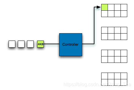
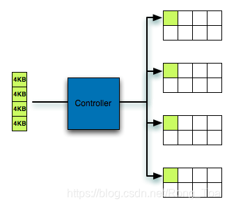
Write-Combining can batches writes to the same cache line so they can be transferred in a single bus clock.

The data will be combined and stored in the write combine buffer, and then write is in burst mode.

By combining small individual memory transfers into one large (and continuous) one. This technique allows systems to nearly saturate the AGP/PCI bus and can transfer twice as much or more data than systems that do not have write combining.

The normal way:

Combine Write

The Weak Ordering problem

Write-Combining is weak ordering which makes it cannot be used for general memory access. The common case to use combine write is deal with frame buffer of video memory which does not need strong ordering.

Using _mm_stream_si128 intrinsics

In C++ code, there are some intrinsics function can help to utilize the write combine buffers.

void _mm_stream_si128(__m128i *p, __m128i a)

Stores the data in a to the address p without polluting the caches. If the cache line containing address p is already in the cache, the cache will be updated. Address p must be 16-byte aligned.

The cache line is the unit of CPU cache and memory transfer. CPU cache implemented by hash map, each bucket is typically 64 bytes. This is so called cache line.

A variable of type __m128i maps to the XMM[0-7] registers. Every register has 128 bits(16 bytes).

Store Intrinsics

Reference

Write-combining

Why SSDs Care About What You Write: Fragmentation & Write Combining

The basic idea of write combining

Copying Accelerated Video Decode Frame Buffers

Write Combining by Martin Thompson


As an AI language model, I do not have the capability to provide you with a specific FPGA DMA RTL code, but I can provide you with a general idea of what an FPGA DMA RTL code might look like. DMA (Direct Memory Access) is a technique used in computer systems to allow devices to transfer data between themselves and memory without the need for the CPU to be involved in the transfer. This is accomplished by using a dedicated DMA controller that has direct access to the system memory. In an FPGA system, the DMA controller can be implemented in RTL (Register Transfer Level) code. The RTL code for the DMA controller typically includes the following components: 1. DMA Controller State Machine: A state machine is used to control the operation of the DMA controller. The state machine has different states such as idle, read, write, etc. depending on the type of transfer that is being performed. 2. Address Generator: The address generator is used to generate the memory addresses for the data transfer. It can be used to increment the memory address after each transfer or to jump to a specific memory location. 3. Data Transfer Logic: The data transfer logic is responsible for transferring the data between the device and the memory. This can be implemented using block RAM or FIFOs. 4. Interrupt Logic: The interrupt logic is used to generate an interrupt signal to the CPU when the data transfer is complete. 5. Configuration Registers: The configuration registers are used to configure the DMA controller. This includes setting the transfer size, transfer direction, and the memory address. The above components are combined together to form the DMA controller RTL code. The DMA controller can be connected to the device and the memory using AXI (Advanced eXtensible Interface) or other interface standards. The DMA controller can also be customized to support different types of devices and memory architectures.
评论 3
添加红包

请填写红包祝福语或标题

红包个数最小为10个

红包金额最低5元

当前余额3.43前往充值 >
需支付:10.00
成就一亿技术人!
领取后你会自动成为博主和红包主的粉丝 规则
hope_wisdom
发出的红包
实付
使用余额支付
点击重新获取
扫码支付
钱包余额 0

抵扣说明:

1.余额是钱包充值的虚拟货币,按照1:1的比例进行支付金额的抵扣。
2.余额无法直接购买下载,可以购买VIP、付费专栏及课程。

余额充值