


 文章探讨了固态硬盘(SSD)中的并行性层次,包括平面并行、通道并行和位向并行,这些机制提升了I/O性能并隐藏了闪存读写操作的延迟。同时,文章也讨论了FTL(闪存转换层)在地址映射、磨损均衡和垃圾回收中的作用,以及通道数量和FTL对SSD功耗的影响。
Analytical Model of SSD Parallelism
Analytical Model of SSD Parallelism
An SSD is a complex device consisting of flash chips, micro-controller, e.g., ARM, memory, which is DRAM or SRAM, and host interface, e.g., SATA or PCIe. The software component of an SSD is called Flash Translation Layer (FTL). It is responsible for (i) translating a logical address into physical address, (ii) evenly distributing the wear-outs, and (iii) consolidating (recliaming) the invalid pages. In designing an SSD, it is very important that all design parameters, e.g., the number of channels, the number of ways, physical page size, address translation algorithms, garbage collection algorithms, wear leveling algorithms etc., are determined, properly incorporating the interactions among these components and the SSDs’ workload characteristics (or target usage).
An SSD consists of a number of physical components, e.g., NAND chips, bus, micro-controllers. These components work independently (or in a synchronized manner) which yields multiple concurrent activities in the device. A latency of an I/O request is governed by the concurrent processing of this I/O request among a number of SSD components.
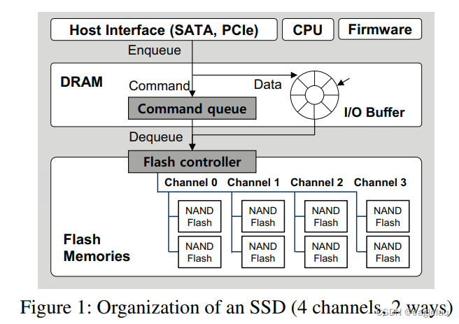
SSDs exploit various levels of IO parallelism, such as plane parallelism, channel parallelism, and way parallelism, to boost up the I/O performance and to hide latency of flash write and read operations.
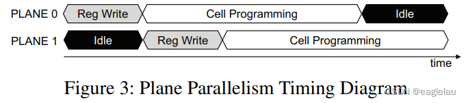
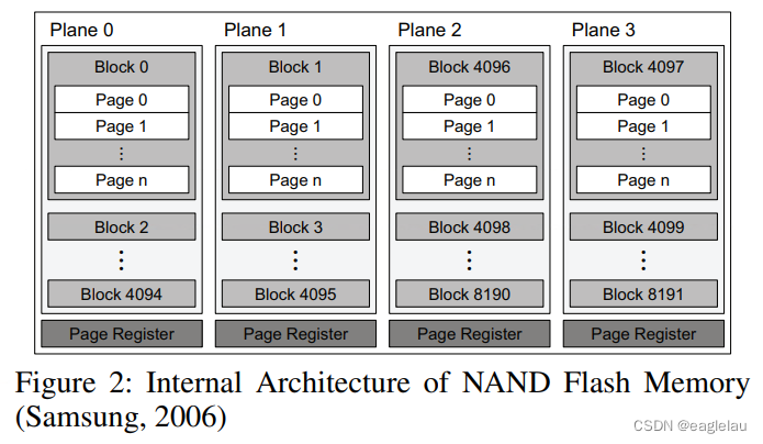
Plane Parallelism: The internal IO behavior of flash memory can be implemented in parallel by using multiple registers at the same time. Since the data transfer time between the flash controller and a register (82usec for Samsung NAND flash (Samsung, 2006)) is much shorter than the programming time of the flash page (900usec for Samsung NAND flash (Samsung, 2006)), the two-page programming operation can be conducted in parallel. This is called ‘plane parallelism’. Figure 3 shows the timing diagram of plane parallelism. Plane parallelism can also be used for read operations.
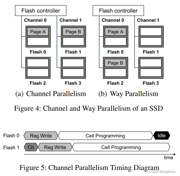
Channel Parallelism: Using several channels, the flash controller concurrently processes multiple IOs. This is called ‘channel parallelism’. Before the flash controller writes data to Flash 1, channel switching delay, denoted as Ch, occurs. Because channel switching delay is sufficiently short (33usec (Yoo et al., 2011)), the flash controller can write the pages to each flash memory at about the same time.
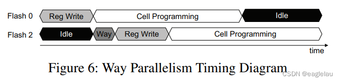
Way Parallelism: Flash memories in the same channel can process IOs in parallel. This is called ‘way parallelism’. In Figure 4(b), the flash controller can utilize way parallelism using Flash 0 and 2 in Channel 0. Because the flash memories share the same channel, a flash memory in the channel can transfer data with flash controller only if the channel is not occupied by another flash memory operation. Before the start of Page B operation, way switching delay(Way) occurs because Flash 0 and Flash 2 are connected to different ways. After way switching delay, the flash controller transfers Page B data to Flash 2 and then Flash 2 starts page write operation.
By using these kinds of IO parallel methods, SSDs achieve higher IO bandwidth.
We define the term IO latency as the time interval between the arrival of the IO command from the host to the device and the time when the I/O device sends the IO interrupt notifying the completion of an IO command. Terms used in each IO latency model are listed in Table 1.
Intel X-25M主流SSD规格:
- 容量 80 GB 和 160 GB
- NAND 闪存组件 英特尔® 多层单元 (MLC) NAND 闪存
- 具有 10nm MLC ONFI 34 NAND 的 1.0 并行通道架构
- 带宽持续顺序读取:高达 250 MB/s
- 持续顺序写入:高达 70 MB/s(80 GB 驱动器)和高达 100 MB/s(160 GB 驱动器)
- 读取延迟:65 微秒
- 写入延迟:85 微秒
- 随机 4 KB 读取:高达 35,000 IOPS
- 随机 4 KB 写入:80 G X25/X18-M – 高达 6,600 IOPS
- 随机 4 KB 写入:160 G X25/X18-M – 高达 8,600 IOPS
- 接口 SATA 1.5 Gb/s 和 3.0 Gb/s
- X25-M:2.5¨ 行业标准硬盘外形尺寸
- 7 毫米 – 76 克 +/- 2 克
- 9.5 毫米 – 80 克 +/- 2 克
- 兼容性 SATA 修订版 2.6 兼容。 兼容 SATA 3 Gb/s,带本机命令队列和 SATA 1.5 Gb/s 接口速率
- 预期寿命 1.2 万小时 (MTBF)
- 活动功耗:150 mW(典型值)
- 空闲 (DIPM):典型值 75 mW
- 工作冲击 1,500 G/0.5 毫秒
- 工作温度 0°C 至 +70°C
Influence of number of channels and ftl on ssd power consumption.
2012 Influence of number of channels and ftl on ssd power consumption.
This paper analyzes the influence of channel among SSD hardware factors and FTL among firmware on SSD power consumption.
2012 Analytic Modeling of SSD Write Performance.
Analytic Modeling of SSD Write Performance


 1945
1945

 被折叠的 条评论
为什么被折叠?
被折叠的 条评论
为什么被折叠?
 到【灌水乐园】发言


