


 本文详细介绍了ADMA2和ADMA3的工作原理及操作流程,包括寄存器编程顺序、地址与长度要求、状态转换等,并阐述了停止/继续功能在不同状态下的实现方式。
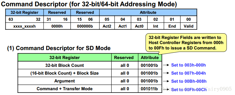
the Host Driver should program these registers sequentially from 000h to 00Fh. The beginning register offset may be calculated based on the type of transaction. The last written offset shall be always 00Fh because writing to the upper byte of the Command register shall trigger issuance of an SD command.
The Host Driver should not read the SDMA System Address, Block Size and Block Count registers during a data transaction unless the transfer is stopped because the value is changing and not stable.To prevent destruction of registers using data transfer when issuing command, the 32-bit Block Count,Block Size, 16-bit Block Count and Transfer Mode registers shall be write protected by the Host Controller while Command Inhibit (DAT) is set to 1 in the Present State register. (When Host Version 4
Enable =0, the SDMA System Address is not protected by this signal.) The Host Driver shall not write the Argument and Command registers while Command Inhibit (CMD) is set to 1.
Writing Command register triggers off ADMA2 transfer. ADMA2 fetches one descriptor line and execute it. This procedure is repeated until end of descriptor is found (End=1 in attribute).
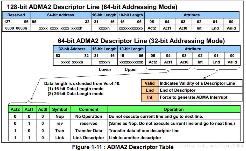
General Descriptor Table Format
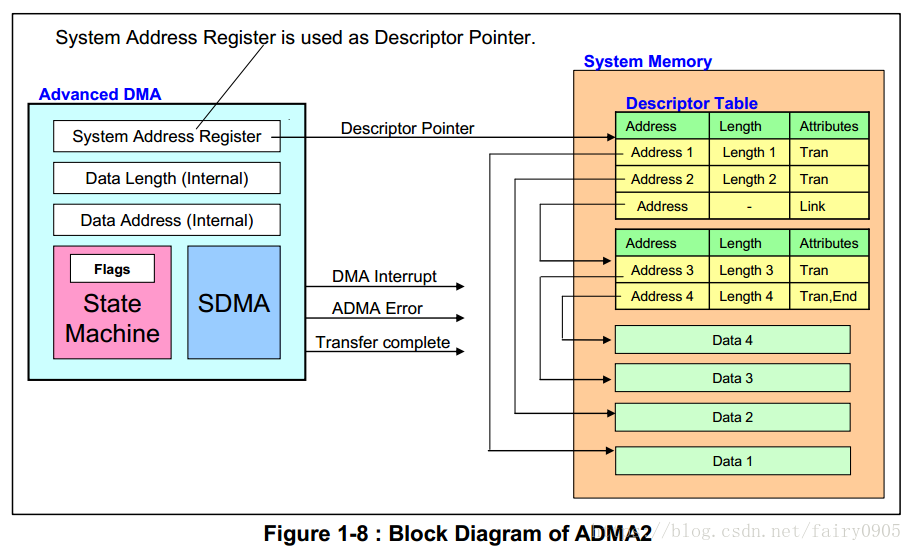
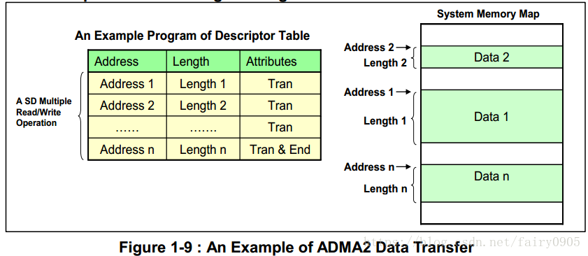
Figure 1-9 shows a typical ADMA2 descriptor program. The Host Driver describes the Descriptor Table with each slice is placed somewhere in contiguous system memory. The Host Driver describes the Descriptor Table with set of address, length and attributes. Each sliced data is transferred in turns as programmed in descriptor.
Data Address and Data Length Requirements
There are three requirements to program the descriptor.
(1) The minimum unit of address is 4 bytes.
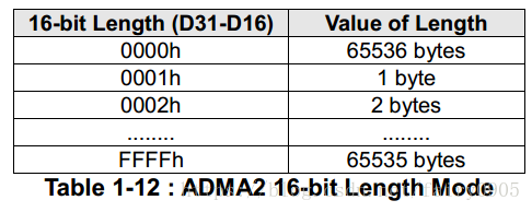
(2) The maximum data length of each descriptor line is less than 64KB.
(3) Total Length = Length 1 + Length 2 + Length 3 + ... + Length n= multiple of Block Size
If total length of a descriptor were not multiple of block size, ADMA2 transfer might not be terminated. In this case, data timeout would occur and the transfer would be stopped by abort command. Therefore, total length should be multiple of block size.
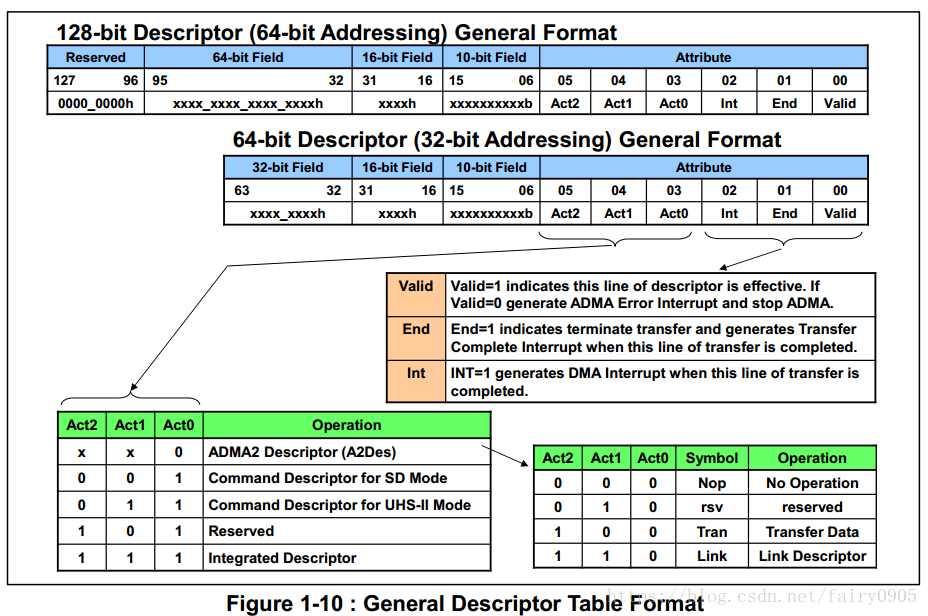
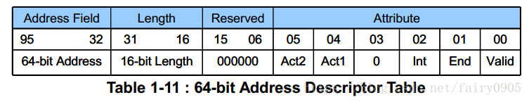
Address registers are defined as 64-bit to support 64-bit addressing. 32-bit address is stored in the lower 32-bit of 64-bit address register. 64-bit and 96-bit Descriptor shall be aligned to 4-byte address boundary (Lower 2-bit of system address is always 0) and 128-bit Descriptor shall be aligned to 8-byte address boundary (Lower 3-bit of system address is always 0).
ADMA2 Descriptor Format
Figure shows ADMA2 Descriptor Table. Act0=0 is assigned to ADMA2 descriptor. Three action symbols are specified by combination of Act2 and Act1. "Nop" operation skips current descriptor line and fetches next one. "Tran" operation transfers data designated by address and length field. "Link" operation is used to connect separated two descriptors. The address field of link points to next Descriptor Table. The combination of Act2=0 and Act1=1 is reserved and defined the same operation as Nop. A future version of controller may use this field and redefine a new operation.
ADMA2 States
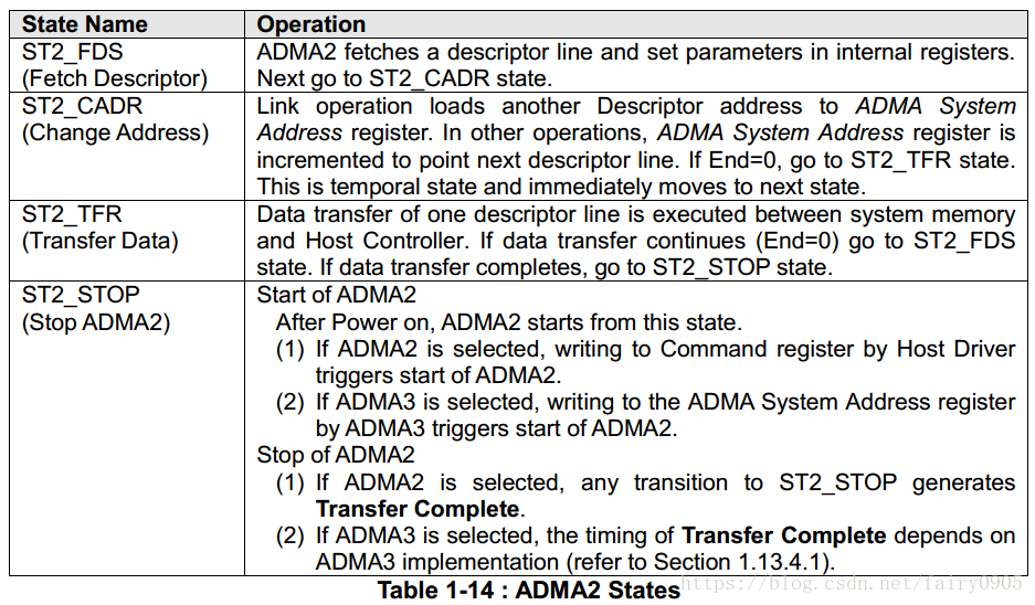
Figure 1-12 shows state diagram of ADMA2. 4 states are defined; Fetch Descriptor state, Change Address state, Transfer Data state and Stop ADMA2 state. Operation of each state is explained in Table 1-14.
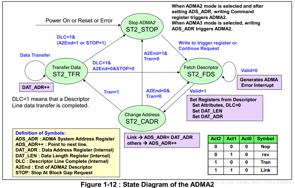
ADMA2 may be initialized when it is triggered by writing the ADMA System Address register.
Stop/Continue Function during ADMA2
"Stop/Continue" is a function to halt data transfer on the way at the block gap of SD bus and to restart data transfer. The Stop At Block Gap Request in the Block Gap Control register is used to halt ADMA2 data transfer and Continue Request in the Block Gap Control register is used to restart ADMA2 data transfer. While stopping ADMA2, any SD command cannot be issued if intending to continue ADMA2 operation (An abort command may be issued and ADMA2 shall be aborted accordingly). The Host Controller stops read operation on SD bus by using Read Wait or stopping SD Clock (In case of Host Controller Version 1.00, the Stop At Block Gap Request can be used with the Read Wait). Host Controller generates the Transfer Complete interrupt when data transfer halts and sets the Block Gap Event when data transfer is not completed yet together with the Transfer Complete. Setting the Continue Request restarts data transfer (Block Gap Event=0 means ADMA2 data transfer is
completed and continue request is not required).
Section 3.12.3 and Section 3.12.4 define Stop/Continue timing for non-DMA. The timing of the Transfer Complete and the Block Gap Event may be different in case of DMA because interrupt timing depends on the relation between data transfer on SD bus and ADMA2 data transfer on system bus (system memory). There may be a difference in data length transferred on SD bus and system bus. In this case, buffer in the Host Controller holds untreated data.
(a) On receiving Stop At Block Gap Request, ADMA2 halts data transfer by transition from ST2_TFR to in ST2_STOP after execution of a descriptor line is completed. Data transfer may halt at any block gap and at any descriptor line where ADMA2 can easily stop. This means that ADMA2 may control the timing of setting STOP symbol to 1 after the Stop At Block Gap Request is set to 1.(b) On receiving Continue Request, ADMA2 restarts data transfer by transiting ST2_STOP to ST2_FDS.
Another simplified implementation is allowed instead of using STOP condition in Figure 1-12, that is, Stop/Continue function may be controlled in ST2_TFR without state transition. This means that ADMA2 may halt and continue during middle of a descriptor line.
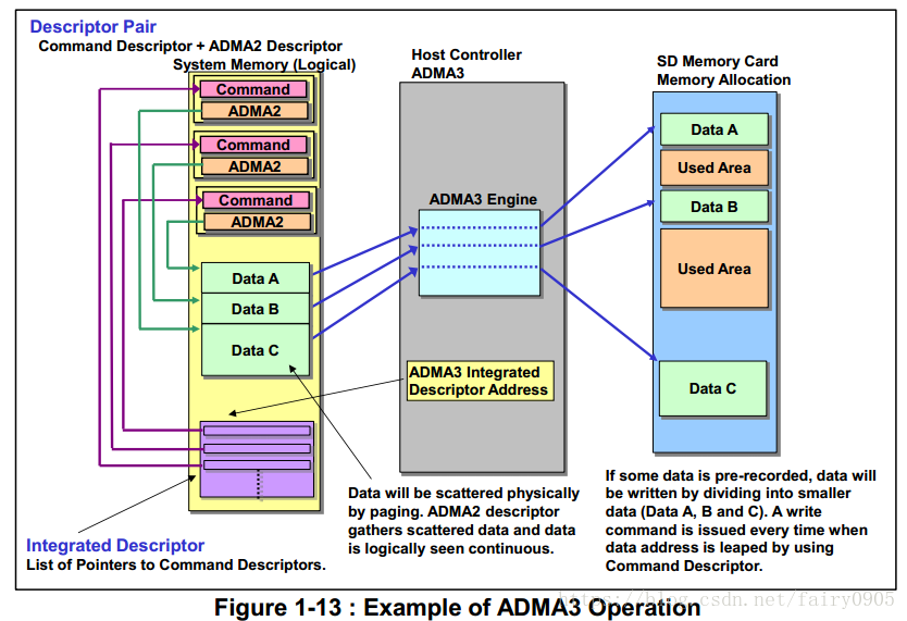
ADMA3
ADMA3 uses Command Descriptor to issue an SD command. A multi-block data transfer between system memory and SD Card is programmed by using a pair of Command Descriptor and ADMA2 Descriptor.ADMA3 performs multiple of multi-block data transfer by using Integrated Descriptor. ADMA3 is optional and support of ADMA3 is indicated by ADMA3 Support in the capabilities register.
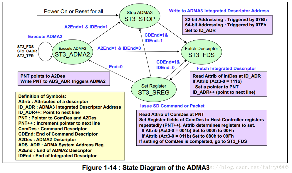
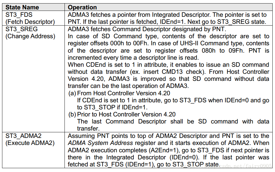
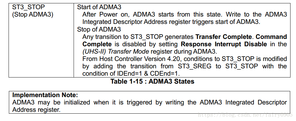
ADMA3 States
Command Descriptor Format


 1217
1217

 被折叠的 条评论
为什么被折叠?
被折叠的 条评论
为什么被折叠?
 到【灌水乐园】发言


