


一直以来,这些电源电压(Vdd 和 Vss)或(Vcc 和 Vee)的命名都有点耐人寻味,甚至令人困惑。但为什么呢?
| It has always been a bit intriguing and even confusing the nomenclature of these power supply voltages (Vdd and Vss) or (Vcc and Vee). But Why? |
一图胜千言:
| The following pictures are worth a thousand words… |
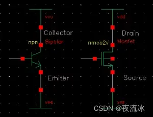
VDD, VSS, Vcc and Vee in Cadence
meaning of VDD VSS VCC and VEE in electronics
现在通常用 Vdd 和 Vss 分别表示正电压和负电压。 Vdd 通常为 5 伏,但现在是 3.3 伏或更低的 1.8 伏或 1.2 伏。Vss 指的是零伏。
| Nowadays it is always used Vdd and Vss to refer to the positive and negative voltage respectively. Vdd is normally was used to be 5V but nowadays is 3.3V or even lower 1.8V or 1.2V. Vss is referred to be zero volts. |
但当我在高中和初学电子学时,Vcc 是正电压(通常为 5 伏),Vee 是接地端。后来,当我们接触到一些电路时,我们会发现引脚 Vss 和 Vdd。也许很多人对此并不感兴趣,但如果你正在阅读这篇文章,你可能会感兴趣。让我们继续:
| But when I learnt electronics in the high school and during my first years of electronics, that Vcc is the positive voltage (usually 5 volts) and Vee was the ground terminal. Later when we get to some circuits we find pins Vss and Vdd. Maybe many have not been intrigued by this but if you are reading this probably yes. So let’s continue: |
这些术语什么意思?
这取决于电子设备内部微芯片、电路或微控制器的晶体管类型。
-
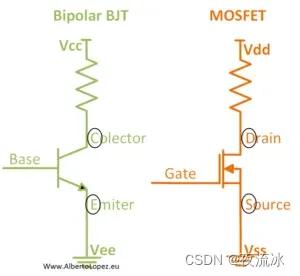
如果内部采用双极晶体管 (BJT),则术语为
-Vcc 表示施加在晶体管集电极上的电压
-Vee 表示施加到晶体管发射极的电压
-
如果内部采用场效应晶体管(FET、MOSFET),则术语为
-Vss 表示施加到晶体管源极引脚的电压。
-Vdd 表示施加到晶体管漏极的电压
| What is the nomenclature? This depends on the type of transistors that the electronic device has internally the microchip, circuit or microcontroller.
–Vcc for being the voltage applied to the Collector of the transistors –Vee for being the voltage applied to the transistor Emitter leg
–Vss for being the voltage applied to the transistor Source pin –Vdd for being the voltage applied to the Drain of the transistors |
那么,每个晶体管的极性是什么?
因为 NPN 和 NMOS 晶体管是用作基准的:
Vcc 和 Vdd 为正电源电压
Vee 和 Vss 为负电源电压或接地。
| So what is the polarity of each one? Because NPN and NMOS transistors are used as a reference: Vcc and Vdd are positive power voltages Vee and Vss are Negative power voltages or are connected to ground. |
为什么是双字母?
让我们来看看一些流行的解释:
1,它源自二进制符号系统。在二进制中,一位数字代表 2 的幂。因此,这表示更高的功率水平。
2,双字母 "dd "或 "ss "符号有助于将电源连接与电路图中的其他信号节点区分开来,从而明确它们作为电压源或电压基准的用途。例如,在晶体管的特定端子(如 Vds)之间,可以使用 "dd "或 "ss"。
| Why the double letter? Well, it is not really crear… let’s see some popular proposed explanations: 1. It is derived from the binary notation system. In binary, a single digit represents a power of 2. Then, a double letter represents a higher power of 2 in terms of voltage. So, this would indicate higher power levels. 2. The notation of doule “dd” or “ss” is to help to distinguish the power supply connections from other signal nodes in a circuit diagram, providing a clear indication of their purpose as voltage sources or voltage references. For example, between specific terminal of the transistors like Vds. |
简而言之...
这是电子电路中电源电压的一种约定俗成的表述方式,有其历史渊源而非逻辑原因。
Vdd 和 Vss 符号已被业界广泛认可和接受,成为所有电子电路中表示电源电压的标准,无论采用的是 MOSFET 还是双极技术。
| In a Nutshell… This is a convention to refer to power supply voltages in electronics circuits has historical origins rather than a logic reason. The Vdd and Vss notations have become widely recognized and accepted as standard in the industry for representations of power supply voltages in all the electronic circuits, regardless the technology is MOSFET or bipolar. |
I hope this will be useful to you!
参考:
https://miscircuitos.com/what-are-the-meaning-of-vdd-vss-vcc-vee-and-gnd/


 1万+
1万+

 被折叠的 条评论
为什么被折叠?
被折叠的 条评论
为什么被折叠?
 到【灌水乐园】发言


