Virtuoso IC618-带隙基准

带隙基准


带隙基准原理

带隙基准电压源模块是产生一个与温度,工艺无关的基准电压;将两个温度系数相反的电压通过一个合适的权重相加,可以得到温度系数为零的基准电压。基准电压V_REF:V_REF=aV_1+bV_2
在半导体工艺各种不同的器件参数中,双极型晶体管的特性参数可以提供正温度系数和负温度系数,双极型晶体管具有以下两个特性:
1.双极型晶体管的基-射极电压V_BE(PN结二极管的正向电压)具有与绝对温度成反比的特性。
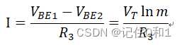
2.在不同的集电极电流情况下,两个双极型晶体管的基-射极电压差值ΔV_BE与绝对温度成正比。

带隙基准结构

在这里插入图片描述
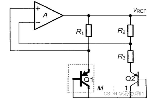
利用放大器两个输入端的电压相近就可以很方便得将正负温度系数特性结合起来,所以电阻R_3承担了双极晶体管基极-发射极电压的差值ΔV_BE,通过下式可以得到流过电阻R_3的电流为:
在这里插入图片描述

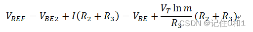
此电流流经电阻R3,R2和晶体管Q2,所以零温度系数的基准电压可以用如下公式求得:
V_REF=V_BE2+I(R_2+R_3 )=V_BE+(V_T  ln⁡m)/R_3 (R_2+R_3)
只要设置合适的电阻R3,2R和m的值就可以达到设计目标.
以上结构电路可以得到的输出电压与温度的关系一般是开口向上的抛物线或开口向下的抛物线,这样就很容易想到如果再叠加一定的曲线,那么就可以进一步消除输出电压的温度效应,使电压更加稳定。

基准电压的产生

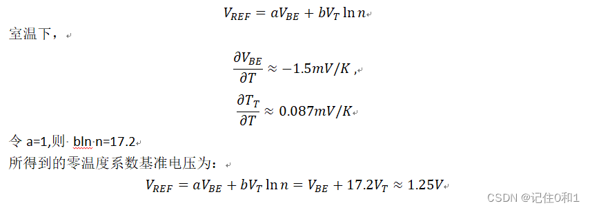
将得到的负温度系数V_BE和正温度系数ΔV_BE分别乘以一个合适的权重系数,再求和。得到一个与温度无关的电压:
在这里插入图片描述
后续。。。

  • 1
    点赞
  • 4
    收藏
    觉得还不错? 一键收藏
  • 打赏
    打赏
  • 1
    评论
### 回答1: Cadence Virtuoso IC618是一款电路设计和仿真软件,主要用于集成电路设计和验证。它具有强大的功能和灵活的设计工具,可以帮助工程师快速设计和验证复杂的电路。该软件支持多种技术节点和工艺,可以满足不同领域的设计需求。 ### 回答2: Cadence Virtuoso IC is a widely used electronic design automation (EDA) tool suite for integrated circuit (IC) design. It is a powerful and comprehensive software package with an intuitive graphical user interface that enables the design of analog, mixed-signal, and RF circuits. Virtuoso IC is a part of the Cadence Design Systems suite of software for electronic design automation (EDA) and is used by many design engineers in the industry. Features and capabilities of Cadence Virtuoso IC include schematic capture, layout design, simulation, verification, and design rule checking. It also provides extensive library of devices and models which helps designers to reduce the design time and improve the accuracy of their designs. Virtuoso IC allows designers to implement their designs with a high degree of precision and sophisticated algorithms. This allows for the design, analysis, and optimization of complex analog and mixed-signal circuits. Virtuoso IC also simplifies the task of designing custom ICs by providing a comprehensive set of features required to build complex mixed-signal designs. The software is also highly optimized for use with large designs, allowing it to handle the complex requirements of today's high performance digital and analog designs. In summary, Cadence Virtuoso IC618 is a sophisticated EDA tool that can help designers to create analog, mixed-signal, and RF circuits. It provides an extensive library of devices and models and allows designers to implement their designs with a high degree of precision. With its powerful features and capabilities, Virtuoso IC is an indispensable tool for designing and verifying complex electronic circuits. ### 回答3: Cadence Virtuoso IC618是一款专业的集成电路设计软件,它是Cadence公司推出的Virtuoso系列软件中的一个版本。该软件可以用于设计各种类型的集成电路,包括模拟电路、数字电路、射频电路等等。 Cadence Virtuoso IC618具有多种功能和特点,其中最突出的包括: 1.高效的设计环境:该软件具有直观且易于使用的用户界面,内置了各种不同的设计工具和快捷方式,使设计师可以更加有效率地完成设计任务。 2.集成的继电器级别的电路模拟器:通过内置的电路模拟器,Cadence Virtuoso IC618可以对电路进行全面的仿真和测试,以确保设计的可靠性和性能。 3.强大的元件库:该软件内置了大量的元件库,涵盖了各种类型的集成电路所需的所有元件,设计师可以根据需要自由选择并使用这些元件。 4.广泛的生产准备功能:Cadence Virtuoso IC618具有广泛的生产准备功能,包括电路布图、电路规则检查、封装设计等等,可以为设计师提供完整的生产准备流程。 总之,Cadence Virtuoso IC618可以为设计师提供全面的集成电路设计解决方案,使他们能够更加高效、可靠地完成设计任务,并最终生产出高质量的集成电路产品。

“相关推荐”对你有帮助么?

  • 非常没帮助
  • 没帮助
  • 一般
  • 有帮助
  • 非常有帮助
提交
评论 1
添加红包

请填写红包祝福语或标题

红包个数最小为10个

红包金额最低5元

当前余额3.43前往充值 >
需支付:10.00
成就一亿技术人!
领取后你会自动成为博主和红包主的粉丝 规则
hope_wisdom
发出的红包

打赏作者

Leon在努力啊

你的鼓励将是我创作的最大动力

¥1 ¥2 ¥4 ¥6 ¥10 ¥20
扫码支付:¥1
获取中
扫码支付

您的余额不足,请更换扫码支付或充值

打赏作者

实付
使用余额支付
点击重新获取
扫码支付
钱包余额 0

抵扣说明:

1.余额是钱包充值的虚拟货币,按照1:1的比例进行支付金额的抵扣。
2.余额无法直接购买下载,可以购买VIP、付费专栏及课程。

余额充值