


USART(Universal Synchronous Asynchronous Receiver Transmitter) 也就是通用同步异步收发。它根据NRZ非同步串行数据工业标准,提供了灵活的全双工数据交换功能。它支持同步单向通信和半双工单线通信,也支持LIN(局部互连网),智能卡协议和IrDA(红外数据组织)SIR ENDEC规范,以及硬件控制操作(需要增加两个管脚,分别是CTS/RTS)。
这里我只简单讲讲如何用USART模块来实现标准EIA-232 串口通讯。
我们首先使用的是硬件控制,然后以中断方式实现了uart数据的收发。
1.uart管脚和clk初始化很简单,整个流程如下:
int main(){
      /* System Clocks Configuration *
      // 1)相应的时钟初始化
      RCC_Configuration(); /

      /* Configure the GPIO ports */
      // 2) 相应的GPIO初始化
      GPIO_Configuration();

        /* USART2 configuration ------------------------------------------------------*/
  /* USART2 configured as follow:
        - BaudRate = 115200 baud
        - Word Length = 8 Bits
        - One Stop Bit
        - No parity
        - Hardware flow control enabled (RTS and CTS signals)
        - Receive and transmit enabled
  */
  // 3) uart数据结构初始化
  USART_InitStructure.USART_BaudRate = 115200;
  USART_InitStructure.USART_WordLength = USART_WordLength_8b;
  USART_InitStructure.USART_StopBits = USART_StopBits_1;
  USART_InitStructure.USART_Parity = USART_Parity_No ;
  USART_InitStructure.USART_HardwareFlowControl = USART_HardwareFlowControl_RTS_CTS;
  USART_InitStructure.USART_Mode = USART_Mode_Rx | USART_Mode_Tx;

  USART_Init(USART2, &USART_InitStructure);
  /* Enable the USART2 */
  USART_Cmd(USART2, ENABLE);

}
1) 对寄存器AFIO_EVCR,AFIO_MAPR和AFIO_EXTICRX进行读写操作前,应当首先打开AFIO的时钟。参考第6.3.7节APB2外设时钟使能寄存器(RCC_APB2ENR)。然后打开相应uart的clock
void RCC_Configuration(void)
{
  /* Enable GPIOx and AFIO clocks */
  RCC_APB2PeriphClockCmd(RCC_APB2Periph_GPIOx | RCC_APB2Periph_AFIO, ENABLE);

  /* Enable USART2 clocks */
  RCC_APB1PeriphClockCmd(RCC_APB1Periph_USART2, ENABLE);
}
2) 对Uart相关的GPIO的设置
/**
  * @brief  Configures the different GPIO ports.
  * @param  None
  * @retval None
  */
void GPIO_Configuration(void)
{
  GPIO_InitTypeDef GPIO_InitStructure;

#if defined(USE_STM3210B_EVAL) || defined(USE_STM32100B_EVAL)
  /* Enable the USART2 Pins Software Remapping */
  GPIO_PinRemapConfig(GPIO_Remap_USART2, ENABLE);
#endif

  /* Configure USART2 RTS and USART2 Tx as alternate function push-pull */
  GPIO_InitStructure.GPIO_Pin = GPIO_RTSPin | GPIO_TxPin; //RTS,TX设置为输出
  GPIO_InitStructure.GPIO_Speed = GPIO_Speed_50MHz;
  GPIO_InitStructure.GPIO_Mode = GPIO_Mode_AF_PP;
  GPIO_Init(GPIOx, &GPIO_InitStructure);

  /* Configure USART2 CTS and USART2 Rx as input floating */
  GPIO_InitStructure.GPIO_Pin = GPIO_CTSPin | GPIO_RxPin; //CTS,RX设置为输入
  GPIO_InitStructure.GPIO_Mode = GPIO_Mode_IN_FLOATING;
  GPIO_Init(GPIOx, &GPIO_InitStructure);
}
3) uart数据结构初始化
  USART_InitStructure.USART_BaudRate = 115200; //比特率
  USART_InitStructure.USART_WordLength = USART_WordLength_8b; //数据宽度
  USART_InitStructure.USART_StopBits = USART_StopBits_1; //
  USART_InitStructure.USART_Parity = USART_Parity_No ; //
  USART_InitStructure.USART_HardwareFlowControl = USART_HardwareFlowControl_RTS_CTS;//硬件控制模式
  USART_InitStructure.USART_Mode = USART_Mode_Rx | USART_Mode_Tx;//接收发送

  USART_Init(USART2, &USART_InitStructure);
  /* Enable the USART2 */
  USART_Cmd(USART2, ENABLE);
以上说明了简单的硬件控制的uart初始化流程。以下说明STM32F10x uart的寄存器。
2.STM32F10x uart寄存器说明
1)status register(USART_SR)
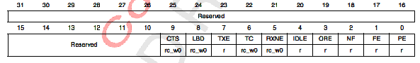
(1) Bit 9 CTS: 如果CTSE比特被设置了的话,这一位会在CTS管脚被拉高之后被设置。这一位需要软件去清零。根据这一位的值,可以判断CTS管脚的值。
0 : nCTS管脚没有变化
1:nCTS管脚有过变化
在nCTS管脚变化的时候,如果USART_CR3的CTSIE=1的话,是会产生一个中断。
当然这都是硬件控制的部分,所以USART4和USART5是不支持的。
(2) LBD : LIN break detection flag
如果检测到LIN break,这一位会被硬件设置为1,而且需要软件去清零。
如果USART_CR2的LBDIE=1的话会产生一个中断。
0 : LIN Break 没有被检测到
1: :LIN Break 有被检测到
(3) TXE: Transmit data register empty
如果TDR register被发送到shift register,TXE位会被设置为1。 而且如果USART_CR1的TXEIE=1的话,是会产生中断的。如果往USART_DR寄存器里写东西,这一位会被清零。
0: data is not transferred to the shift register
1: data is transferred to the shift register
(4) TC: Transmissino complete
如果一个一帧(frame)的数据传输完毕,而且TXE被设置为1了的话,这一位会被设置为1。如果USART_CR1的TCIE=1的话,是会产生中断的。这一位会被连续的软件操作给清零(往USART_DR写,紧接着再从USART_SR寄存器读),当然这种操作只是在multibuffer通信的时候才推荐的。TC寄存器也可以软件写0请清楚。
0:Transmission is not complete
1:Transmission is complete
(5) RXNE: Read data register not empty
如果RDR shift register的内容已经传送到USART_DR,则这个值就会被设置。如果USART_CR1的RXNEIE=1,则会有中断产生。读USART_DR寄存器,会清楚这个寄存器。
当然RXNE这位也可以软件清零,但这种方式只是在multibuffer通信的时候才推荐。
(6) IDLE: IDLE line detected
如果IDLE line被检测到,则硬件会设置这一位。如果USART_CR1的IDLEIE=1的话,设置这一位的同时会产生一个中断。软件操作会清楚这一位(读USART_DR,紧接着写USART_SR)。
(7) ORE:Overrrun error
如果当前收到的shift register的内容准备好可以传送给RDR register,且RXNE=1的时候,ORE这一位就会被硬件设置为1。如果USART_CR1的RXNEIE=1,则会产生一个中断。这位会被下列软件操作清零(读USART_DR,紧接着读USART_DR)
0: No Overrun error
1: Overrun error is detected
注:这位被设置为1,RDR register不会丢失但shift register会被覆盖。
(8) NF: Noise detected flag
如果收到的帧检测到噪声,这一位就会被设置。这一位会被如下软件操作清零(读USART_DR,紧接着读USART_SR)
(9) FE: Framing error
这一位在同步失败(de-synchronization),噪音超标或者数据损坏的时候被设置。读USART_DR,紧接着读USART_SR会清零。
0: No framing error is detected
1: Framing error or break character is detected
(10) PE: Parity error
parity error(奇偶校验失败??)的时候,这一位就被设置为1。读写USART_DR,紧接着读status register会把这位清零。
2) Data Register(USART_DR) 数据的读写都用这个寄存器
Address offset: 0x04
Reset value: 0xXXXXXXXX
Bits 31:9 Reserved, must be kept at reset value.
Bits 8:0 DR[8:0] : Dava value
保存着读或者写的内容。这个寄存器既可以用来读,也可以用来写是因为这个寄存器是TDR和RDR两个寄存器的组合。
如果parity使能(奇偶校验使能)的话(USART_CR1的PCE被设置),DR寄存器中的MSB(bit 7或者是bit8 ,这取决于数据的长度)是没有意义的,因为这位会被parity给取代。同理,如果parity使能了,从DR[8:0]里读出来的MSB也是parity bit,不是数据。
3) Baud Rate Register( USART_BRR)
4) Control register (USART_CR1)
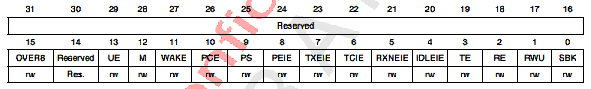
(1) OVER8: Oversampling mode
0: oversampling by 16
1: oversampling by 8
(2) UE: USART enable
USART使能位,这一位可以被软件设置和清零
(3) M: Word length
这一位表示数据长度,这一位可以被软件设置或清零
0: 1 Start bit, 8 Data bits, n Stop bit
1: 1 Start bit, 9 Data bits, n Stop bit
注:这一位不应该在数据传输过程中修改
(4) WAKE: Wakeup method
表示wakeup method,可以被软件修改
0: Idle Line
1: Address Mark
(5) PCE: Parity control enable
这一位选择parity control(generation and detection)。 如果parity control使能了,计算出来的parity会被写到MSB位置(9th bit if M=1; 8th bit if M=0),且接收到的数据会被检查parity。这一位可以被软件设置或清零。
0: parity control disabled
1: parity control enabled
(6) PS: Parity selection
如果parity generation/detection使能的话(PCE bit set),会根据PS选择是奇数还是偶数校验。
0: Even parity
1: Odd parity
(7) PEIE: PE interrupt enable
这位可以被软件读写
0: interrupt is inhibited
1: An USART interrupt is generated whenever PE=1 in the USART_SR register.
(8) TXEIE : TXE interrupt enable
This bit is set and cleared by software.
0: Interrupt is inhibited
1: An USART interrupt is generated whenever TXE=1 in the USART_SR register
(9) TCIE: Transmission comple te interrupt enable
This bit is set and cleared by software.
0: Interrupt is inhibited
1: An USART interrupt is generated whenever TC=1 in the USART_SR register
(10) RXNEIE: RXNE interrupt enable
This bit is set and cleared by software.
0: Interrupt is inhibited
1: An USART interrupt is generated whenever ORE=1 or RXNE=1 in the USART_SR register
(11)IDLEIE: IDLE interrupt enable
This bit is set and cleared by software.
0: Interrupt is inhibited
1: An USART interrupt is generated whenever IDLE=1 in the USART_SR register
(12) TE: Transmitter enable
This bit enables the transmitter. It is set and cleared by software.
0: Transmitter is disabled
1: Transmitter is enabled
(13) RE: Receiver enable
This bit enables the receiver. It is set and cleared by software.
0: Receiver is disabled
1: Receiver is enabled and begins searching for a start bit
(14) RWU: Receiver wakeup
This bit determines if the USART is in mute mode or not. It is set and cleared by software
and can be cleared by hardware when a wakeup sequence is recognized.
0: Receiver in active mode
1: Receiver in mute mode
Note: 1: Before selecting Mute mode (by setting the RWU bit) the USART must first receive a
data byte, otherwise it cannot function in Mute mode with wakeup by Idle line detection.
2: In Address Mark Detection wakeup conf iguration (WAKE bit=1) the RWU bit cannot
be modified by software while the RXNE bit is set.
(15) SBK: Send break
This bit set is used to send break characters. It can be set and cleared by software. It should
be set by software, and will be reset by hardware during the stop bit of break.
0: No break character is transmitted
1: Break character will be transmitted
5) Control register 2 (USART_CR2)
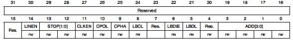
(1) LINEN: LIN mode enable
可以被软件读写
0: LIN mode disabled
1: LIN mode enabled
The LIN mode enables the capability to send LIN Synch Breaks (13 low bits) using the SBK bit in
the USART_CR1 register, and to detect LIN Sync breaks.
(2) STOP: STOP bits
These bits are used for programming the stop bits.
00: 1 Stop bit
01: 0.5 Stop bit
10: 2 Stop bits
11: 1.5 Stop bit
(3) CLKEN: Clock enable
This bit allows the user to enable the SCLK pin.
0: SCLK pin disabled
1: SCLK pin enabled
(4) CPOL: Clock polarity
This bit allows the user to select the polarity of the clock output on the SCLK pin in synchronous
mode. It works in conjunction with the CPHA bit to produce the desired clock/data relationship
0: Steady low value on SCLK pin outside transmission window.
1: Steady high value on SCLK pin outside transmission window.
(5) CPHA : Clock phase
This bit allows the user to select the phase of the clock output on the SCLK pin in synchronous
mode. It works in conjunction with the CPOL bit to produce the desired clock/data relationship (see
figures 308 to 309 )
0: The first clock transition is the first data capture edge
1: The second clock transition is the first data capture edge
(6) LBCL : Last bit clock pulse
This bit allows the user to select whether the clock pulse associated with the last data bit
transmitted (MSB) has to be output on the SCLK pin in synchronous mode.
0: The clock pulse of the last data bit is not output to the SCLK pin
1: The clock pulse of the last data bit is output to the SCLK pin
(7) LBDIE : LIN break detection interrupt enable
Break interrupt mask (break detection using break delimiter).
0: Interrupt is inhibited
1: An interrupt is generated whenev er LBD=1 in the USART_SR register
(8) LBDL : lin break detection length
This bit is for selection between 11 bit or 10 bit break detection.
0: 10-bit break detection
1: 11-bit break detection
(9) ADD[3:0]: Address of the USART node
This bit-field gives the address of the USART node.
This is used in multiprocessor communication during mute mode, for wake up with address mark
detection.
6) Control register 3( USART_CR3)
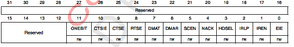
(1) ONEBIT: One sample bit method enable
This bit allows the user to select the sample method. When the one sample bit method is
selected the noise detection flag (NF) is disabled.
0: Three sample bit method
1: One sample bit method
(2) CTSIE : CTS interrupt enable
0: Interrupt is inhibited
1: An interrupt is generated whenever CTS=1 in the USART_SR register
(3) CTSE: CTS enable
0: CTS hardware flow control disabled
1: CTS mode enabled, data is only transmitted when the nCTS input is asserted (tied to 0).
If the nCTS input is deasserted while a data is being transmitted, then the transmission is
completed before stopping. If a data is written into the data register while nCTS is asserted,
the transmission is postponed until nCTS is asserted
(4) RTSE: RTS enable
0: RTS hardware flow control disabled
1: RTS interrupt enabled, data is only requeste d when there is space in the receive buffer.
The transmission of data is expected to cease after the current character has been
transmitted. The nRTS output is asserted (tied to 0) when a data can be received
(5) DMAT : DMA enable transmitter
This bit is set/reset by software
1: DMA mode is enabled for transmission.
0: DMA mode is disabled for transmission
(6) DMAR : DMA enable receiver
This bit is set/reset by software
1: DMA mode is enabled for reception
0: DMA mode is disable for reception
(7) SCEN : Smartcard mode enable
This bit is used for enabling Smartcard mode.
0: Smartcard Mode disabled
1: Smartcard Mode enabled
(8) NACK : Smartcard NACK enable
0: NACK transmission in case of parity error is disabled
1: NACK transmission during parity error is enabled
(9) HDSEL: Half-duplex selection
Selection of Single-wire Half-duplex mode
0: Half duplex mode is not selected
1: Half duplex mode is selected
(10) IRLP: IrDA low-power
This bit is used for selecting between normal and low-power IrDA modes
0: Normal mode
1: Low-power mode
(11) IREN : IrDA mode enable
This bit is set and cleared by software.
0: IrDA disabled
1: IrDA enabled
(12) EIE: Error interrupt enable
Error Interrupt Enable Bit is required to enable interrupt generation in case of a framing
error, overrun error or noise flag (FE=1 or ORE=1 or NF=1 in the USART_SR register) in
case of Multi Buffer Communication (DMAR=1 in the USART_CR3 register).
0: Interrupt is inhibited
1: An interrupt is generated whenever DMAR=1 in the USART_CR3 register and FE=1 or
ORE=1 or NF=1 in the USART_SR register
在调试过程中,注意CTS和RTS的管脚设置试PULL DOWN, PULL UP,NO PULL。设置不对会导致无法上拉RTS或者没有检测到CTS被拉高,无法通信。


 3087
3087

 被折叠的 条评论
为什么被折叠?
被折叠的 条评论
为什么被折叠?
 到【灌水乐园】发言


