


1 CoreSight Overview
1.0 非正式定义
CoreSight,顾名思义就是核心视野。通过CoreSight就可以查看芯片内部的情况。可以用来进行芯片调试。例如,通过CoreSight就可以查看或者操纵内核寄存器。
1.1 CoreSight出现的背景
1.1.1 CoreSight出现之前的Debug方案
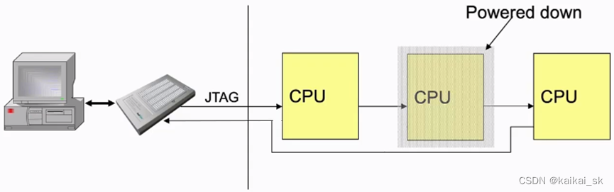
多CPU通过菊花链(Daisy Chain)的方式连接到主机。
存在问题:一旦某个设备power down之后,整体都不可用。
1.1.2 CoreSight出现之前的Trace方案
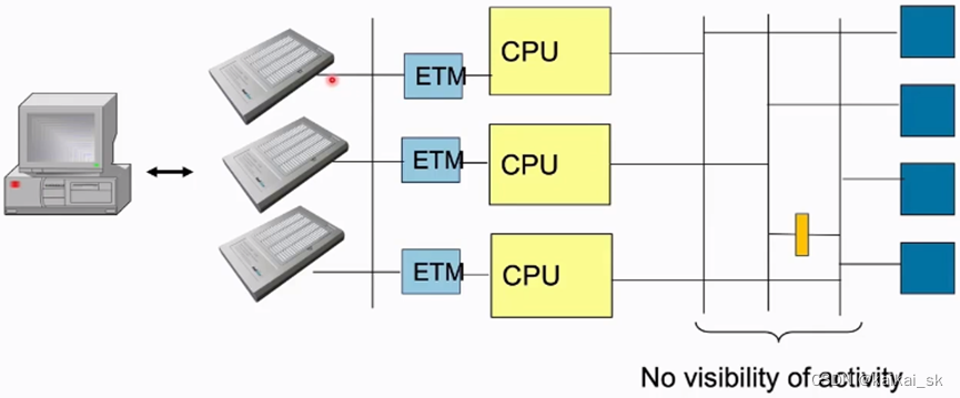
Expensive(pin-count) to implement multi trace ports. 每一个CPU都需要一个Trace端口,多个CPU就需要多组端口。
Difficult to combine trace output for off chip delivery.
ETMs only give view of CPU activity: problem may lie elsewhere.
1.2 CoreSight定义
1.2.1 定义
为了解决传统解决方案在多核SOC芯片上的限制而提出的高级调试和跟踪解决方案。
CoreSight架构规范进行描述。
1.2.2 功能
一个Debugger连接就可以访问系统中所有的processors、内存映射设备和存储器。
系统中多个Trace源共享一个Trace端口。(多个AP,一个DP。不同的核对应不同的AP)。
2 Components & Buses
2.1 Overview
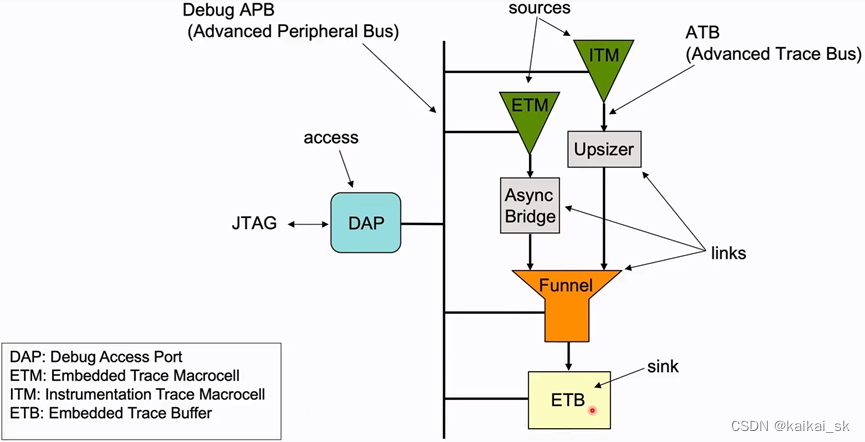
ETM和ITM属于Trace源。ITM一般就是用来提供打印的能力,一般可以用来自定义printf。ETM一般就是用来记录CPU指令执行的信息。
Upsizer和异步桥属于Trace Links。ITM一般输出是8 bit信号, 但是funnel的接收的输入都是32bit,所以需要upsizer来调整位宽。异步桥用来解决跨时钟域的问题,ETM一般和CPU是用一个clock,和系统时钟是同频的。但是Funnel作为CoreSight的组件,可能使用的是CoreSight的时钟,二者时钟频率是不一样的。 Funnel的作用就是将多路输入合并成一路数据。
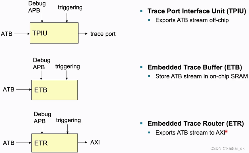
ETB属于Trace Sink。是个Buffer用来缓存数据的。
2.1.1 复杂系统Examples
2.2 Debug APB&ATB总线
都符合AMBA(Advanced Microcontroller Bus Architecture)协议
Debug APB:AMBA 3高级外设总线
ATB:(1)AMBA 3高级Trace总线(2)类似于AMBA AXI写channel。 ATB是单向的总线。
2.3 Trace Sources
2.3.1 xTM
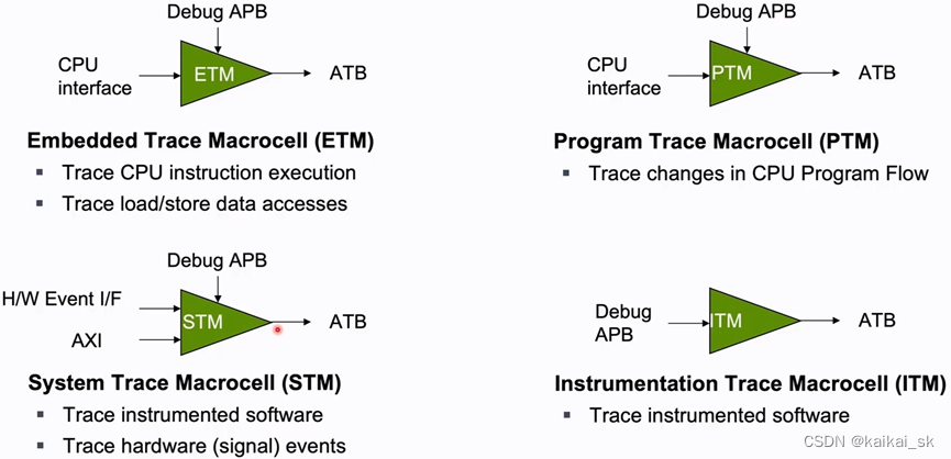
ETM:比较常见和传统的。 一般很少trace数据,因为数据量太大,很容易产生overflow。
PTM:默认程序是顺序执行的。只记录发生跳转或者异常的时候的情况。
STM:功能类似于ITM。但是速率会比ITM高很多。 AXI协议比Debug APB要快很多,吞吐也会高很多。STM一般用于A系列,ITM一般用于M系列。 STM可用作硬件信息的Monitor。
2.4 Trace Links
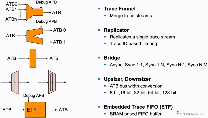
Funnel: 多路变成一路
Replicator:一路变成多路。 变多路的用处就是可以送到不同的sink那里去。 比如说ITM数据就可以发送到SWO也可以发动到TPIU。 Trace ID就是Trace source的ID,用来区分Trace的来源。
ETF:FIFO buffer。用于减少数据溢出。
2.4 Trace Sinks
2.5 Timestamp
Trace Source生成包的时候都需要使用时间戳,都需要将时间戳加到data packets里面。
时间戳的作用:
(1)可以体现不同Trace源的数据 的时间相关性。
(2)使用单个跟踪源的数据进行近似的基于时间的分析
所有的Trace sources都使用一个通用的timestamp generator。
2.6 ROM Table
2.6.1 overview
ROM table内含有debug组件的信息。
- 具有单个调试组件的系统不需要 ROM 表。然而,设计人员可能会选择实现这样的系统以包含 ROM 表。
- 超过一个调试组件的系统必须含有至少一个ROM table。
**ROM 表连接到由内存访问端口 (MEM-AP) 控制的总线。**换句话说,ROM 表是连接到 MEM-AP 的存储器系统的地址空间的一部分。一条总线上可以连接多个 ROM 表。
2.6.2 ROM Table类型
Arm® 调试接口架构规范 (ADIv6.0) 中的以下类型的 ROM 表允许与符合 CoreSight 版本 3.0 的组件一起使用:
Class 0x1 ROM Tables:
• The Component class field, CIDR1.CLASS, is 0x1, which identifies the component as a Class
0x1 ROM Table.
• The PIDR4.SIZE field must be 0.
• A ROM Table must occupy a single 4KB block of memory.
• A Class 0x1 ROM Table is a read-only device.
Class 0x9 ROM Tables:
• The Component class field, CIDR1.CLASS, is 0x9, which identifies the component as a
CoreSight Component.
• The DEVTYPE and DEVID registers contain information about the ROM Table.
• The PIDR4.SIZE field must be 0.
• A ROM Table must occupy a single 4KB block of memory.
• Class 0x9 ROM Table entries are 32 or 64 bits wide.
注意:0x9 类 ROM 表可以与 0x1 类 ROM 表一起使用,并且 0x9 类和 0x1 类 ROM 表都可能存在于符合 CoreSight v3 的系统中。
2.6.3 Component and Peripheral ID Registers for ROM Tables
Any ROM Table must implement a set of Component and Peripheral ID Registers, that start at offset 0xFD0 in the
ROM Table.
2.6.3.1 Identifying the debug SoC, system, or subsystem
ROM 表中的唯一组件标识符(Unique Component Identifier)唯一标识 ROM 表描述的 SoC、平台(Platform)或子系统(subsystem)。例如:
- 与指向所有组件的 ROM 表层次结构分组在一起的组件簇由簇中最外层 ROM 表唯一标识。
- 连接到单个 MEM-AP 的所有组件的子系统由子系统中最外层的 ROM 表唯一标识。该ROM表通常是MEM-AP指向的第一个组件。
- SoC 由多个实现 ADIv5 的 MEM-AP 组成,由来自每个内存访问端口指向的所有最外层 ROM 表的集体唯一组件标识符来唯一标识。
- SoC 由多个实现 ADIv6 的 MEM-AP 组成,由最外层 ROM 表中的唯一组件标识符唯一标识,该表提供每个 MEM-AP 的指针。该ROM表通常是DP指向的第一个组件。
SoC、系统或子系统在构建时可能是可配置的。例如,处理器集群可能允许处理器的数量是可配置的。描述此类组件集合的 ROM 表对于系统的所有配置可能具有相同的唯一组件标识符。然而,这仅在包括或排除组件时才允许,并且当地址映射中任何组件的位置改变或组件的功能显着改变时不允许相同。实际上,ROM表唯一组件标识符唯一地标识组件集合的超集配置。具有相同唯一组件标识符的 ROM 表可能仅描述此超集的子集。
3 CoreSight编程模型

每一个CoreSight组件都是至少有4KB的地址空间来定义和分布自己的寄存器。
0xF00到0xFFF的地址空间一般定义一些Identification的寄存器,用来标识组件的类型等信息。0x000到0xF00一般就会定义一些控制寄存器和状态寄存器。
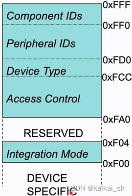
Component ID:就是组件的类型。
Peripheral ID:serial number, version号。
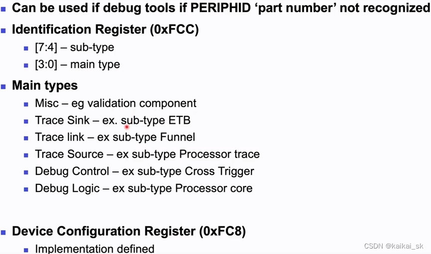
Device Type:它是ETM还是ETB?
Integration Mode:集成模式。 通过集成模式的寄存器可以直接控制CoreSight模块的输出值。 这个主要是用于检测拓扑结构,也就是数据通路是否通畅。
3.1 Component ID
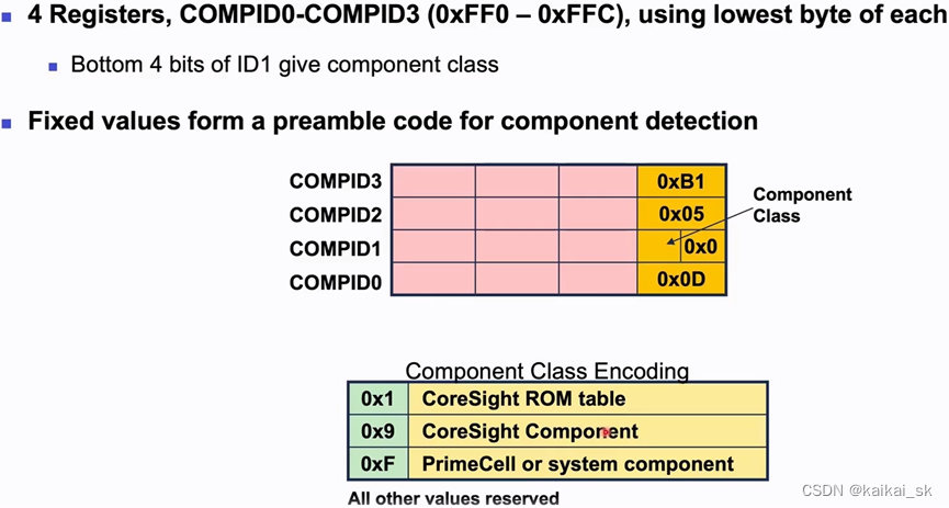
ID0,2,3这三个寄存器的值是固定的。 ID1是有区别的。 如果ID1的最后一个byte是0x1,那么它就是ROM table。
3.2 Peripheral ID
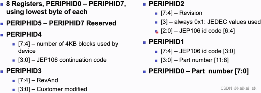
JEP106,每一个芯片公司都有它自己的ID。
一般ROM Table扫描出来的JEP106就是具体的设计芯片的公司。 如果是其他CoreSight组件的JEP 106一般就会指向ARM。
3.3 Device Type
4 使用场景
4.1 ROM Table

4.2 Debug Monitor中断
- 使能中断
		// 测试debug monitor中断
		// enable debug monitor
		CoreDebug->DEMCR |= (1 << 16);
		NVIC_EnableIRQ(DebugMonitor_IRQn);
		NVIC_SetPriority(DebugMonitor_IRQn, 1);
- 实现中断响应函数
void DebugMon_Handler(void) {
		printf("DebugMon_Handler entered\n");
}

void HardFault_Handler() {
		printf("HardFault_Handler entered\n");
}
如果没有进debug monitor handler,而是进了hard fault handler,那么就说明Debug Monitor没有使能。
- 中断触发条件
程序实现软件断点,全速run起来的情况下可以进去debug monitor中断。
#if defined (TEST_SOFTWARE_BREAKPOINTS)
		// 测试软件断点
		imtprintf("start test software breakpoint.\r\n");
	    __asm("BKPT 0"); imtprintf("software breakpoint 1\r\n");
		__asm("BKPT 0"); imtprintf("software breakpoint 2\r\n");
        __asm("BKPT 0"); imtprintf("software breakpoint 3\r\n");
		__asm("BKPT 0"); imtprintf("software breakpoint 4\r\n");
	    __asm("BKPT 0"); imtprintf("software breakpoint 5\r\n");
		__asm("BKPT 0"); imtprintf("software breakpoint 6\r\n");
		__asm("BKPT 0"); imtprintf("software breakpoint 7\r\n");
		__asm("BKPT 0"); imtprintf("software breakpoint 8\r\n");
#endif
4.2.1 参考资料
[1] https://developer.arm.com/documentation/ddi0337/e/CEGHJDCF
[2] https://interrupt.memfault.com/blog/cortex-m-debug-monitor
[3] https://blog.csdn.net/kaikai_sk/article/details/136150814
4.3 Programming the cross halt
Cross-halt behavior happens when one processor core enters the Halting debug state, and then all the processor cores should enter the Halting debug state. This is a common situation that is encountered when debugging a system.
To generate the cross-halt behavior, the debugger must make use of the Debug Halt and Cross Halt trigger events. The debug halt event is the signal to the processor core to enter the debug state. The cross-halt event is the signal from the processor core that it is entering the debug state. To achieve the cross-halt behavior, the debugger maps the debug halt event and cross halt event signals for every processor core in the system to the same cross-trigger channel. For example, if the debugger mapped the events to Channel 3 it would program the registers as follows:
• Enable the CTI: CTICONTROL = 0b1
• Map input trigger 0 to Channel 3: CTIINEEN0 = 0b1000
• Map output trigger 0 to Channel 3: CTIINEEN0 = 0b1000
• Enable event propagation on Channel 3: CTIGATE = 0b1XXX
The following diagram illustrates how Trigger inputs 0 and Trigger outputs 0 for multiple CTI components can be mapped to channel 3 of the Cross Trigger Matrix:

注意:需要programme LAR寄存器,clear software lock。否则向CTI_CONTROL寄存器中写值的话会失效,即,值写不进去,写了在读出来还是没有变化。
4.3.1 编程实现
(1)enable trace 功能
CoreDebug -> DEMCR |= CoreDebug_DEMCR_TRCENA_Msk;
(2)清除CTI的软件访问锁
LOCK_ACCESS_REGISTER = 0xC5ACCE55
(3)enable CTI功能
CTI_CONTROL |= (1 << 0);
(4)enable要使用的channel
CTI_GATE |= (1 << 3); // 这里使用了channel 3
(5)建立trigger和channel的映射
// 这里是trigger 0 和channel 3 建立映射。
CTI_IN_EN0 |= (1 << 3);
CTI_OUT_EN0 |= (1 << 3);
2.2.2 参考资料
[1] https://developer.arm.com/documentation/102520/0100/Programming-the-cross-halt
2.3 CTI中断
CTI中断是由ctitrigout信号触发产生。 ctitrigoutack信号可以清除ctitrigout所影响的寄存器的值。
配置【Integration Test Trigger Output register, ITTRIGOUT】寄存器相应的trigger为的值为1,可以产生ctitrigout信号。channel中也可以产生ctitrigout信号,可以通过配置【CTI Application Pulse register, CTIAPPPULSE】的值,在指定的channel上产生一个channel Event,会将此event传递给相应的trigger。
配置【CTI Interrupt Acknowledge register, CTIINTACK】的值可以acknowledge ctitrigout信号。
2.3.1 编程实现
2.3.1.1 准备工作
(1)enable trace功能和CTI的功能。
(2)启用想要使用的channel。下图所示,就启用了channel 3.
(3)建立trigger和channel的映射。以K3芯片为例,只有trigger2和trigger1才能产生中断信号给中断控制器,所以下图讲trigger2和channel3绑定。
(4)使能中断
2.3.1.2 触发中断
在channel 3上面产生channel Event,即可给trigger 2发出ctitrigout信号,触发中断。
CTI_APP_PULSE |= (1 << 3);
2.3.1.3 中断响应
(1)实现中断相应函数
(2)在相应函数中清除中断。避免频繁进入中断响应函数。
CTI_INT_ACK |= (1 << 2);
2.3.2 参考资料
[1] 《ARM® CoreSight™ SoC-400 Revision: r3p2 Technical Reference Manual》中CTI registers章节
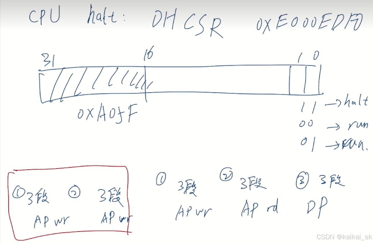
2.4 调试器是如何halt住CPU的
具体操作步骤如下:
a)Write 0xA05F0001 to DHCSR, which halting debug enabled.
b)Write 0x01 to DEMCR. This enable Reset Vector Catch.
c)Write 0xFA050004 to AIRCR. This reset the core.
现在,内核将在第一条指令时暂停,所有外围设备和寄存器(调试寄存器除外)都将设置为复位值
2.4.1 参考材料
[1] https://www.zhihu.com/question/312830435/answer/3491276146
5 SWD协议
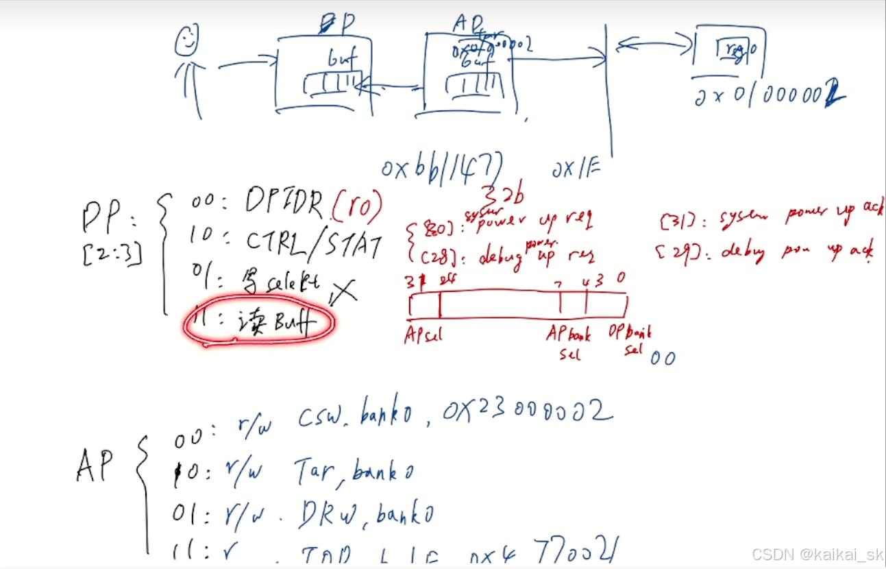
coresight不是单独出现的。 一般coresight + SWD协议 + others 一起组成ADIvx协议。
5.1 SWD包格式
Request + ACK + DATA的三段式格式
5.2 SWD实现具体功能案例
5.2.1 SWD halt住CPU
【向DHCSR寄存器写值来halt住CPU】
(1)三段式请求,写AP.TAR寄存器, 写入DHCSR寄存器的地址,表示要向DHCSR中写值了。
(2)三段式请求,写AP.DRW寄存器,写入要写入的值,表示向DHCSR中写入值。
【读取DHCSR寄存器来确认是否halt住了CPU】
(1)三段式请求,写AP.TAR寄存器, 写入DHCSR寄存器的地址,表示要从DHCSR中读取。
(2)三段式请求,写AP.DRW寄存器,表示从DHCSR中读取。
(3)三段式请求,读取DP.BUFF, 从中真正获取到值。
5.2.2 SWD Reset CPU
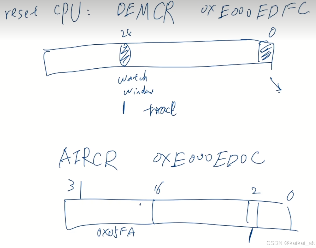
操作这两个寄存器
5.2.3 SWD Connect
【JLINK整个初始化过程】
(1)connect
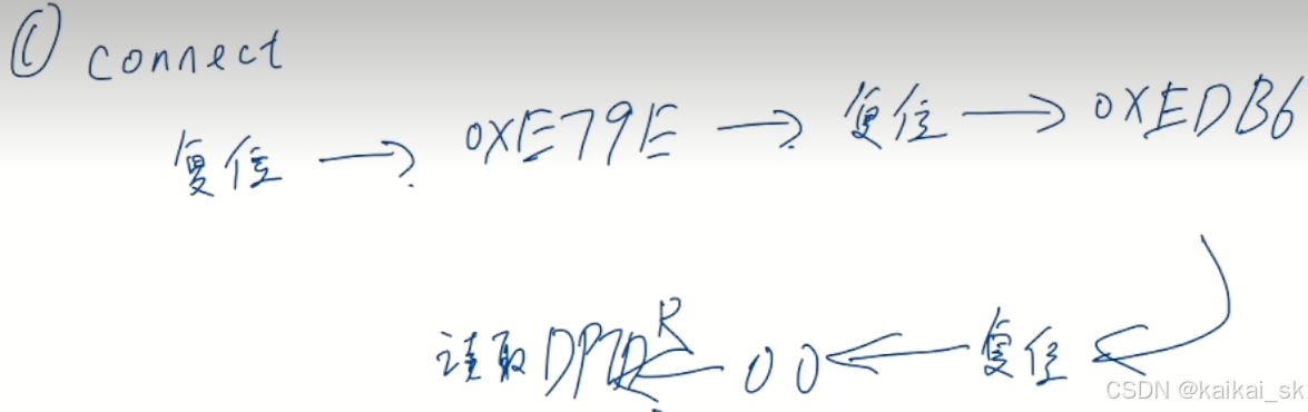
最开始的复位是56个bit的line reset。
(2)给AP上电
power up requeset 和 debug powder up request。
(3)halt住CPU
(4)
5.2.1 SWD设置内核寄存器的值
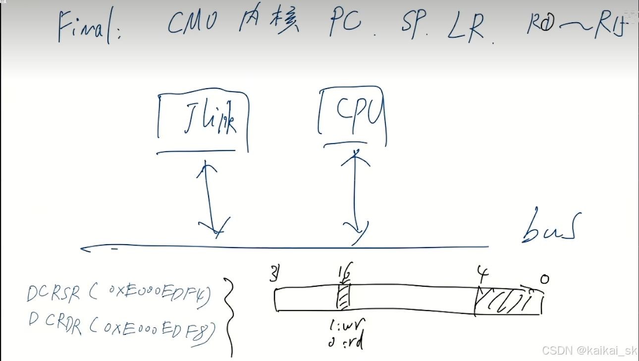
【读取PC的值】
(1)写DCRSR: 指定要读(bit[16]写0), 并且要指定寄存器的编号(bit[4:0]写0xF)。
(2)读取DCRDR:读取上来的值就是PC的值。
【写PC的值】
类似地
5.3 参考资料
[1] https://www.cnblogs.com/snowsad/p/14827794.html#21swd%E9%80%9A%E4%BF%A1%E6%97%B6%E5%BA%8F%E5%88%86%E6%9E%90
[2] https://www.bilibili.com/video/BV1cM4m1U7vA/?spm_id_from=333.999.0.0&vd_source=f4dcb991bbc4da0932ef216329aefb60
[3] https://www.bilibili.com/video/BV1Zf421X7JP/?spm_id_from=333.999.0.0&vd_source=f4dcb991bbc4da0932ef216329aefb60
6 调试相关寄存器
地址 类型 复位值 描述
0xE000EDF0 读写 0x00000000 调试停止控制和状态寄存器(DHCSR)
0xE000EDF4 只写 - 调试内核寄存器的选择寄存器
0xE000EDF8 读写 - 调试内核寄存器数据寄存器
0xE000EDFC 读写 0x00000000 调试异常和监控控制寄存器
6.1 参考资料
[1] https://bbs.eeworld.com.cn/thread-1168927-1-1.html
参考资料
[1] 【从小白到专家!全方位入门Arm CoreSight系统!-哔哩哔哩】 https://b23.tv/M7ONUJe
[2] 《ARM® CoreSight™ SoC-400 Revision: r3p2 Technical Reference Manual》coresight_soc400_technical_reference_manual_100536_0302_01_en.pdf
介绍了SOC400的组件和每一个组件的寄存器
[3] https://www.cnblogs.com/shangdawei/p/4748751.html
[4] https://www.silabs.com/documents/public/application-notes/an0062.pdf
[5] https://www.silabs.com/documents/public/application-notes/an1303-efr32-dci-swd-programming.pdf
[6] https://www.zhihu.com/question/312830435/answer/3491276146
[7] https://repo.lauterbach.com/adarmdbg.html
[8] https://repo.lauterbach.com/adwhisker_mipi20t-hs.html
[9] https://baijiahao.baidu.com/s?id=1783786915309099355&wfr=spider&for=pc


 9196
9196

 被折叠的 条评论
为什么被折叠?
被折叠的 条评论
为什么被折叠?
 到【灌水乐园】发言


