


 ▬▬▬▬▬▶STM32实验内部时钟◀▬▬▬▬▬
⚔️前言
首先说明一下芯片内部并没有时钟, 而是内部振荡。
使用内部振荡的好处是外部无需设计晶振电路
再说的简单点 ,不用外部晶振依然可以让单片机正常运转。
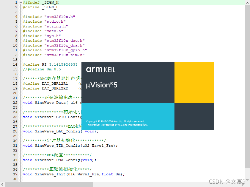
⚔️打开任意keli工程
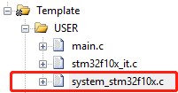
⚔️打开system_stm32f10x.c文件
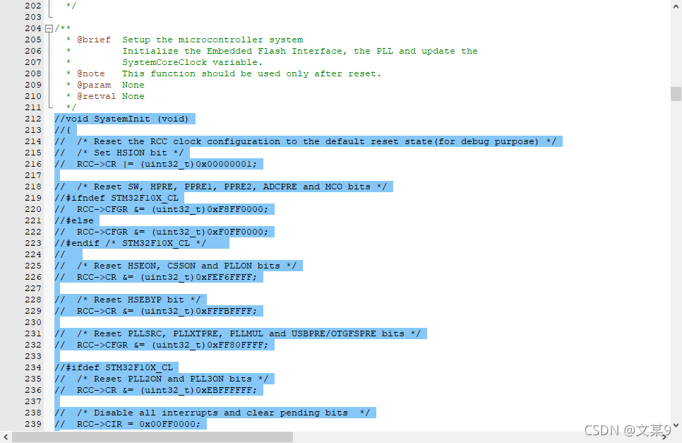
⚔️找到systeminit函数 全部注释掉
⚔️然后在下面粘贴以下代码
直接替换就可以用了!!!
#define  USE_HSI   1			// 是否使用内部晶振  0 不使用  1使用
void SystemInit ( void )
{

#if USE_HSI
    {
//设置使用内部晶振
        /* 开启HSI 即内部晶振时钟 */
        RCC->CR |= ( uint32_t ) 0x00000001;
        /*选择HSI为PLL的时钟源HSI必须2分频给PLL*/
        RCC->CFGR |= ( uint32_t ) RCC_CFGR_PLLSRC_HSI_Div2;
        /*PLLCLK=8/2*9=36MHz  设置倍频得到时钟源PLL的频率*/
        RCC->CFGR |= ( uint32_t ) RCC_CFGR_PLLMULL6; 			//设置倍频后的频率
        /* PLL不分频输出 ?*/
        RCC->CFGR |= ( uint32_t ) RCC_CFGR_HPRE_DIV1;
        /* 使能 PLL时钟 */
        RCC->CR |= RCC_CR_PLLON;
        /* 等待PLL时钟就绪*/
        while ( ( RCC->CR & RCC_CR_PLLRDY ) == 0 )
        {
        }
        /* 选择PLL为系统时钟的时钟源 */
        RCC->CFGR &= ( uint32_t ) ( ( uint32_t ) ~ ( RCC_CFGR_SW ) );
        RCC->CFGR |= ( uint32_t ) RCC_CFGR_SW_PLL;
        /* 等到PLL成为系统时钟的时钟源*/
        while ( ( RCC->CFGR & ( uint32_t ) RCC_CFGR_SWS ) != ( uint32_t ) 0x08 )
        { }
    }
#else
    {
//设置使用外部8M晶振
        /* Reset the RCC clock configuration to the default reset state(for debug purpose) */
        /* Set HSION bit */
        RCC->CR |= ( uint32_t ) 0x00000001;

        /* Reset SW, HPRE, PPRE1, PPRE2, ADCPRE and MCO bits */
#ifndef STM32F10X_CL
        RCC->CFGR &= ( uint32_t ) 0xF8FF0000;
#else
        RCC->CFGR &= ( uint32_t ) 0xF0FF0000;
#endif /* STM32F10X_CL */

        /* Reset HSEON, CSSON and PLLON bits */
        RCC->CR &= ( uint32_t ) 0xFEF6FFFF;

        /* Reset HSEBYP bit */
        RCC->CR &= ( uint32_t ) 0xFFFBFFFF;

        /* Reset PLLSRC, PLLXTPRE, PLLMUL and USBPRE/OTGFSPRE bits */
        RCC->CFGR &= ( uint32_t ) 0xFF80FFFF;

#ifdef STM32F10X_CL
        /* Reset PLL2ON and PLL3ON bits */
        RCC->CR &= ( uint32_t ) 0xEBFFFFFF;

        /* Disable all interrupts and clear pending bits  */
        RCC->CIR = 0x00FF0000;

        /* Reset CFGR2 register */
        RCC->CFGR2 = 0x00000000;
#elif defined (STM32F10X_LD_VL) || defined (STM32F10X_MD_VL) || (defined STM32F10X_HD_VL)
        /* Disable all interrupts and clear pending bits  */
        RCC->CIR = 0x009F0000;

        /* Reset CFGR2 register */
        RCC->CFGR2 = 0x00000000;
#else
        /* Disable all interrupts and clear pending bits  */
        RCC->CIR = 0x009F0000;
#endif /* STM32F10X_CL */

#if defined (STM32F10X_HD) || (defined STM32F10X_XL) || (defined STM32F10X_HD_VL)
#ifdef DATA_IN_ExtSRAM
        SystemInit_ExtMemCtl();
#endif /* DATA_IN_ExtSRAM */
#endif

        /* Configure the System clock frequency, HCLK, PCLK2 and PCLK1 prescalers */
        /* Configure the Flash Latency cycles and enable prefetch buffer */
        SetSysClock();

#ifdef VECT_TAB_SRAM
        SCB->VTOR = SRAM_BASE | VECT_TAB_OFFSET; /* Vector Table Relocation in Internal SRAM. */
#else
        SCB->VTOR = FLASH_BASE | VECT_TAB_OFFSET; /* Vector Table Relocation in Internal FLASH. */
#endif
    }

#endif
}
⚔️项目获取
▬▬▬▬▬▶点击下方◀▬▬▬▬▬


 899
899

 被折叠的 条评论
为什么被折叠?
被折叠的 条评论
为什么被折叠?
 到【灌水乐园】发言


